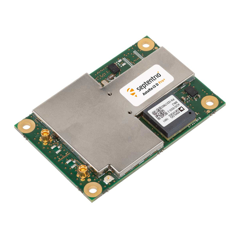
SEPTENTRIO AsteRx-m3 User manual

AsteRx-m3 Product Group
Hardware Manual
Version 2.2.0

2
2
2
AsteRx-m3 Product Group Hardware Manual
Version 2.2.0
May 28, 2021
© Copyright 2000-2021 Septentrio nv/sa. All rights reserved.
Septentrio
Greenhill Campus, Interleuvenlaan 15i
3001 Leuven, Belgium
http://www.septentrio.com
Phone: +32 16 300 800
Fax: +32 16 221 640
@septentrio

3
3
3
1Table of contents
1TABLE OF CONTENTS................................................................................................... 3
2ASTERX-M3 OEM .......................................................................................................... 6
2.1 Mounting .................................................................................................................. 7
2.2 Environmental ......................................................................................................... 7
2.3 Power and Power Consumption ............................................................................ 7
2.4 RF Interface.............................................................................................................. 8
2.4.1 Electrical Specifications .......................................................................................... 8
2.5 I/O Connectors....................................................................................................... 10
2.5.1 30-pin Connector.................................................................................................. 11
2.5.2 60-pin connector................................................................................................... 12
2.6 External Frequency Reference Input (REF IN).................................................... 14
2.7 Frequency Reference Output (REF OUT)............................................................. 14
2.8 Event/TimeSync Inputs......................................................................................... 14
2.9 General Purpose Output (GPx) ............................................................................ 15
2.10 Standby Mode ........................................................................................................ 15
2.11 SD Memory Card Usage ........................................................................................ 16
2.12 USB Interface ......................................................................................................... 17
2.13 Ethernet.................................................................................................................. 17
3ROBOTICS INTERFACE BOARD .................................................................................. 19
3.1 Mechanical Drawings............................................................................................ 20
3.2 USB Dev................................................................................................................... 20
3.3 44-pin Header......................................................................................................... 21
3.4 LEDs......................................................................................................................... 22
3.5 Log Button Header ................................................................................................ 23
3.6 PPS/Event Header.................................................................................................. 23
3.7 Power Supply Options........................................................................................... 23

4
4
4
4DEVELOPMENT KIT .................................................................................................... 25
4.1 Header Types ......................................................................................................... 25
4.2 Powering the DevKit ............................................................................................. 25
4.3 Antenna Connectors ............................................................................................. 26
4.4 LEDs and General Purpose Output Pins ............................................................. 27
4.5 COM Ports............................................................................................................... 27
4.6 PPS Out and Event Inputs..................................................................................... 28
4.7 Ethernet.................................................................................................................. 29
4.8 USB Dev................................................................................................................... 29
4.9 USB Host ................................................................................................................. 29
4.10 REF IN ...................................................................................................................... 29
4.11 Buttons ................................................................................................................... 29
4.12 SD Card Socket ....................................................................................................... 30
APPENDIX A LED STATUS INDICATORS......................................................................... 31
APPENDIX B SYSTEM NOISE FIGURE AND C/N0.......................................................... 33
APPENDIX C EMC CONSIDERATIONS ........................................................................... 34

5
5
5
ROHS/WEEE NOTICE
Septentrio receivers are compliant with the latest WEEE, RoHS and REACH directives. For
more info see www.septentrio.com/en/environmental-compliance.
ESD PRECAUTIONS
The OEM module is sensitive to electrostatic discharge (ESD). Although it has a limited
protection, it should only be manipulated in an ESD-safe environment and using ESD-safe
tools and equipment. These tools are typically marked with the following symbol:

6
6
AsteRx-m3 OEM
6
2AsteRx-m3 OEM
All dimensions in millimeters.
Weight = 27 g
Note: the above pictures and mechanical diagrams show both u.FL and MMCX antenna
connectors. In reality, only one type of connector is available depending on the board
variant.
RF connectors (u.FL or MMCX type) are mounted on top side of the PCB. The 30- and 60-
pin Hirose I/O connectors are mounted on the bottom side.
AUX1
MAIN
REF OUT

7
7
AsteRx-m3 OEM
7
2.1 Mounting
The four mounting holes are compatible with M3 screws. Use M3 3.5mm spacers. An
example of applicable SMD spacer is THF-1.6-3.5-M3 from MAC8.
All mounting holes are grounded, and should preferably be connected to ground on the
host PCB. Note however that the mounting holes should not be relied on as only ground
return connection: a proper ground should be supplied to the GND pins of the I/O
connector(s) as well.
The maximum height of the components at the bottom side of the AsteRx-m3 OEM board
is within the mask shown below. The maximum component height is 1.1mm in the green
area and 1.6mm in the yellow area.
2.2 Environmental
Operational: -40 to +85 °C
Storage: -55 to +85 °C
2.3 Power and Power Consumption
The board is powered through pin#1 and pin#2 of the 30-pin connector. Power supply
voltage must be 3.3V +/-5%.
The power consumption depends on the set of GNSS signals enabled with the
setSignalTracking command.

8
8
AsteRx-m3 OEM
8
The following table shows the typical power consumption for selected sets of signals. The
dual antenna configuration corresponds to a receiver where the option to track from the
AUX1 antenna is enabled.
Signals enabled with setSignalTracking
Power consumption
Dual antenna
Single antenna
GPS L1+L2
1.05 W
0.75 W
GPS L1+L2, GLO L1+L2
1.10 W
0.80 W
All GNSS signals from all GNSS constellations
1.60 W
1.00 W
Enabling the built-in L-Band demodulator with the setLBandSelectMode command adds
100 mW.
Enabling wideband interference mitigation with the setWBIMitigation command adds
160 mW (dual antenna) or 80mW (single antenna).
Consumption in standby mode: 3 mW
Note that the power consumption in the above table are average values. To account for
peak currents, the minimum power supply drive capability should be 1 Ampere.
2.4 RF Interface
For illustration purposes, the above picture shows both u.FL and MMCX connectors. In
reality, only one type of connector is available depending on the board variant.
The main antenna must be connected to the u.FL or MMCX connector marked “MAIN” on
the PCB and the auxiliary antenna must be connected to the AUX1 connector.
2.4.1 Electrical Specifications
Antenna supply voltage
3-5.5V DC, set via pin#18 of the 30-pin connector. The same
voltage is applied to both antennas. If pin#18 is not
connected, there is no DC voltage to the antennas.
DC series impedance
2.7 Ohms
Antenna current limit
150 mA per antenna
Antenna net gain range1
15-50 dB
For optimal performances, the net gain on MAIN and AUX1
must not differ by more than 10dB.
AUX1
MAIN

9
9
AsteRx-m3 OEM
9
Receiver noise figure
10 dB (with 15-dB net gain)
The receiver noise figure increases as the net gain increases,
but its contribution to the system noise figure decreases.
The worse case is for a net gain of 15dB.
RF nominal input impedance
50 Ohms
VSWR
< 2.5:1 in 1200-1251 MHz and 1560-1610 MHz range
1 The net gain is the total pre-amplification of the distribution network in front of the receiver. Typically, this
equals antenna active LNA gain minus coax losses in the applicable GNSS bands.

10
10
AsteRx-m3 OEM
10
2.5 I/O Connectors
The main connector is the 30-pin connector. That connector must always be connected.
The 60-pin connector provides additional signals (IO enable, serial CTS/RTS lines, GPIOs,
Ethernet, 10-MHz reference input, etc). That connector can be ignored and left
unconnected if these signals are not needed.
Warnings
•All ground pins must be connected (not applicable to the 60-pin connector if that
connector is not used).
•Do not drive a non-zero voltage into input pins (pins type “I”in the tables below)
when the receiver is not powered. In addition, if standby mode is applicable, input
pins must remain in high-Z when the IO_EN signal is not set. See section 2.10 for
details.
•When pull-up/down resistors are needed, use 10 k.
•Unused or reserved pins should be left unconnected unless explicitly mentioned
otherwise.
Conventions
•Pin Type: I=Input, O=Output, P=Power, Ctrl=Control, Clk=Reference clock
•LVTTL=3V3 Low Voltage TTL: VIL≤ 0.8V, VIH≥ 2.0V, VOL≤ 0.4V, VOH≥ 2.4V.
•PU: internally pulled up
•PD: internally pulled down
•K: keeper input type
60 pin
30 pin

11
11
AsteRx-m3 OEM
11
2.5.1 30-pin Connector
Connector type: Hirose 30 pins DF40HC (3.5)-30DS-0.4V(51)
Mating connector: Hirose DF40C-30DP-0.4V(51)
See the pin numbering convention in the above picture.
Pin#
Name
Type
Level
Description
Comment
1
Vin
P
3.3V
+/-5%
Main power supply input
Both Vin pins (pin#1 and pin#2) must
be tied together.
3
GND
Gnd
0
Ground.
5
USB_D+
I/O
USB
USB data signal positive D+.
7
USB_Vbus
Ctrl
4.40V
≤V≤
5.25V
USB VBUS.
This pin cannot be used to power the receiver!
Mandatory if USB is used.
See section 2.12
9
TX1
O
LVTTL
Serial COM 1 transmit line (inactive state is high)
11
GND
Gnd
0
Ground.
13
TX2
O
LVTTL
Serial COM 2 transmit line (inactive state is high)
15
TX3
O
LVTTL
Serial COM 3 transmit line (inactive state is high)
17
GND
Gnd
0
Ground.
19
EventA
I, PD
LVTTL
Event A input.
See section 2.8
21
PPS2
O
LVTTL
Second PPS output. Output impedance: 50 ohms. Output current:
24 mA. Polarity and rate user selectable independently of PPS1 on
pin#12. During start up, this pin is floating, See Reference Guide for
operating instructions. Pulse duration controllable with the
setPPS2Parameters command (default: 5ms).
External pull up/down can be used to
impose level during start up.
23
GND
Gnd
0
Ground.
25
Button
I, K
LVTTL
Input can be connected to a push button used to control SD card
logging. Low state is interpreted as “button pressed”.
Debouncing must be done externally
(no debouncing circuit on board).
See also section 2.11.
27
LOGLED
O
LVTTL
Internal logging status indicator.
Max output current: 10 mA; output impedance: 20 Ohms
See Appendix A
29
GND
Gnd
0
Ground.
Pin#
Name
Type
Level
Description
Comment
2
Vin
P
3.3V
+/-5%
Main power supply input
Both Vin pins (pin#1 and pin#2) must be
tied together.
4
GND
Gnd
0
Ground.
6
USB_D-
I/O
USB
USB data signal negative D-.
8
nRST
Ctrl,PU
LVTTL
Reset input, active negative. Receiver resets when driven low.
10
RX1
I, K
LVTTL
Serial COM 1 receive line (inactive state is high).
12
PPS1
O,PD
LVTTL
First PPS output. Output impedance: 50 ohms. Output current: 24
mA. Polarity and rate user selectable. During start up, this pin is
pulled low with a 100-kOhm resistor.
See Reference Guide for operating instructions. Pulse duration
controllable with the setPPSParameters command (default: 5ms).
14
RX2
I, K
LVTTL
Serial COM 2 receive line (inactive state is high).
16
RX3
I, K
LVTTL
Serial COM 3 receive line (inactive state is high).
18
VANT
P
3<
VANT
< 5.5V
Antenna supply.
See section 2.4.1
20
nPDN
Ctrl,PU
LVTTL
Receiver is put in standby mode (low power mode) when driven low.
Normal operation resumes when the pin level is high.
22
GPLED
O
LVTTL
General purpose LED.
Max output current: 10 mA; output impedance: 20 Ohms
See Appendix A
24
Reserved
26
SD_CLK
O
LVTTL
SD card CLK line
See section 2.11
28
SD_CMD
O
LVTTL
SD card CMD line
See section 2.11
30
SD_DAT0
I/O
LVTTL
SD card DAT0 line
See section 2.11
1
29
30
2

12
12
AsteRx-m3 OEM
12
2.5.2 60-pin connector
Connector type: Hirose DF40C-60DP-04V(51)
Mating connector: Hirose DF40HC(3.5)-60DS-0.4V(51)
See the pin numbering convention in the above picture.
Pin#
Name
Type
Level
Description
Comment
1
Reserved
3
Reserved
5
Reserved
7
Reserved
9
GP1
O
LVTTL
General purpose output. GP1 in setGPIOFunctionality command.
See section 2.9
11
RTS2
O
LVTTL
Serial COM2 RTS line. The AsteRx-m3 drives this pin low when ready
to receive data.
13
RTS3
O
LVTTL
Serial COM3 RTS line. The AsteRx-m3 drives this pin low when ready
to receive data.
15
TX4
O
LVTTL
Serial COM 4 transmit line (inactive state is high)
17
Reserved
19
Reserved
21
Reserved
23
Reserved
25
Reserved
27
Reserved
29
GND
Gnd
Ground
31
RMII_TXEN
O
LVTTL
LAN PHY transmit enable
See section 2.13
33
RMII_TXD1
O
LVTTL
LAN PHY transmit data 1
See section 2.13
35
RMII_CRS_DV
I
LVTTL
LAN PHY CRS
See section 2.13
37
RMII_RXER
I
LVTTL
LAN PHY RX error
See section 2.13
39
Reserved
41
Reserved
43
Reserved
45
Reserved
47
Reserved
49
Reserved
51
Reserved
53
Reserved
55
Reserved
57
EventB
I,PD
LVTTL
Event B input.
See section 2.8
59
IO_EN
O
LVTTL
Level is high when board is in normal operating conditions and it is
safe to drive the input pins (see also warnings in section 2.10). This
pin becomes high no later than 300 ms after power up or wake up
from standby.
2
59
1
60

13
13
AsteRx-m3 OEM
13
Pin#
Name
Type
Level
Description
Comment
2
Reserved
4
GND
Gnd
Ground
6
Reserved
8
GND
Gnd
Ground
10
Reserved
12
CTS2
I, K
LVTTL
Serial COM 2 CTS line. Must be driven low when ready to receive
data from the AsteRx-m3.
14
CTS3
I, K
LVTTL
Serial COM 3 CTS line. Must be driven low when ready to receive data
from the AsteRx-m3.
16
RX4
I, K
LVTTL
Serial COM 4 receive line (inactive state is high).
18
GND
Gnd
Ground
20
Reserved
22
Reserved
24
Reserved
26
Reserved
28
Reserved
30
GND
Gnd
Ground
32
RMII_CLK
O
LVTTL
LAN PHY Clock
See section 2.13
34
RMII_TXD0
O
LVTTL
LAN PHY transmit data 0
See section 2.13
36
GND
Gnd
Ground
38
RMII_RXD0
I
LVTTL
LAN PHY receive data 0
See section 2.13
40
RMII_RXD1
I
LVTTL
LAN PHY receive data 1
See section 2.13
42
GND
Gnd
Ground
44
GP2
O
LVTTL
General purpose output. GP2 in setGPIOFunctionality command.
See section 2.9
46
Reserved
48
Reserved
50
GND
Gnd
Ground
52
Reserved
54
MDIO
I/O
LVTTL
LAN PHY control data
See section 2.13
56
MDC
O
LVTTL
LAN PHY control clock
See section 2.13
58
GND
Gnd
Ground
60
REF IN
Clk
10-MHz frequency reference input
AC-coupled, 13-kOhm input impedance, 2-5Vpp
See section 2.6

14
14
AsteRx-m3 OEM
14
2.6 External Frequency Reference Input (REF IN)
An external 10 MHz frequency reference can be fed into the receiver through pin#60 of
the 60-pin connector (REF IN). The 10 MHz signal can be a sine wave or a square wave
with a peak-to-peak amplitude between 2V and 5V, for example it can be an LVTTL clock
signal.
At start-up, the receiver checks the presence of the external frequency reference on
pin#60. If a signal is present, the receiver uses that signal as primary frequency reference,
instead of its internal TCXO. The reference signal must be present on pin#60 at receiver
boot and must remain present at all times during receiver operation.
This feature is under permission. Make sure that the FreqSync permission is enabled if
you need to use the REF IN pin. If the receiver detects a 10 MHz signal on its REF IN pin
and the FreqSync permission is disabled, most output will be blocked.
2.7 Frequency Reference Output (REF OUT)
The frequency reference used by the receiver is available at the REFOUT u.FL connector.
This is a 10MHz square wave, 0 - 2.8V, output impedance 50Ohms.
The REFOUT signal can be enabled or disabled with the setREFOUTMode command. It is
enabled by default.
When an external frequency reference is provided to the REF IN pin (see section 2.6), the
signal at the REF OUT connector is synchronized with the REF IN signal.
2.8 Event/TimeSync Inputs
The receiver features two event inputs (EventA on the 30-pin connector, and EventB on
the 60-pin connector), which can be used to time tag external events with a time resolution
of 20ns. Use the setEventParameters command to configure these pins (e.g. to set the
polarity). Note that this feature requires the TimedEvent permission to be enabled in the
receiver.
If the TimeSync permission is enabled, the event inputs can also be configured as
TimeSync source using the setTimeSyncSource command. When an event pin is
configured as TimeSync source, the receiver expects to see a one-pulse-per-second (PPS)
signal on that pin. It will then synchronize its internal time base (i.e. the time at which
REF OUT

15
15
AsteRx-m3 OEM
15
GNSS measurements are sampled) to that PPS input signal. TimeSync is typically used in
conjunction with REF IN (see section 2.6) to fully synchronize the receiver internal time
base with the time of an external clock.
Note that there is a delay of 15 to 50 ns between the PPS pulse at the TimeSync pin and
the receiver internal time base. That delay is dependent on the phase difference between
the 10 MHz frequency at the REF IN input and the PPS pulse at the TimeSync input. It is
possible to measure this delay by synchronizing the PPS output pulse (PPS1 pin) with the
internal time base, with the setPPSParameters,,,,RxClock command.
2.9 General Purpose Output (GPx)
The GP1 and GP2 pins of the 60-pin connector are general purpose LVTTL digital outputs,
of which the level can be programmed with the setGPIOFunctionality command.
During the first seconds after powering up the board, these pins are in tristate. Use an
external pull-down or pull-up resistor to have the desired level during boot.
The GPx pins can drive a maximum current of 10mA.
2.10 Standby Mode
In standby mode, all receiver functions are turned off and the power consumption is
significantly reduced (see section 2.3). There are two ways to enter standby mode:
1. By driving the nPDN pin low (pin#20 of the 30-pin connector). The receiver wakes
up when the nPDN pin level is high again (there is an internal pull-up).
2. By entering the “exePowerMode, StandBy” user command. To wake up, the nPDN
pin should be shortly driven low (at least for 50ms).
It is also possible to schedule automatic standby/wakeup periods using the
setWakeUpInterval command.
Note that entering standby mode takes a few seconds during which all running processes
are shutdown.
Warning: Do not drive a non-zero voltage into input pins (pins type “I”) when the receiver
is in standby. To be safe during standby, it is recommended to use the IO_EN signal of the
60-pin connector as enable for the drivers driving the input pins. The IO_EN signal is low
during standby.

16
16
AsteRx-m3 OEM
16
2.11 SD Memory Card Usage
The receiver can interface to an external SD memory card through the SD-card pins of the
30-pin connector. The receiver supports the 1-bit SD transfer mode with 3V3 signaling.
An example circuit to a 9-pin SD memory card socket is shown below. The maximum clock
frequency (SD_CLK) is 33.000 MHz.
See instructions in the Reference Guide for details on how to configure SD card logging.
The receiver is compatible with SD cards of up to 32GB. The file system is FAT32.
Shortly driving the button pin (pin#25 of 30-pin connector) low toggles logging on and off.
Driving the button pin low for at least 5 seconds unmounts the SD card if it was mounted,
or mounts it if it was unmounted. The SD card mount status can be checked with the
LOGLED pin (see Appendix A).
When powering off the receiver while logging is ongoing, it can be that the last seconds of
data are lost. To avoid data losses, it is advised to first unmount the SD card. This can be
done in two ways:
1. By entering the command “exeManageDisk, DSK1, Unmount”before turning off
the receiver.
2. By driving the button pin (pin#25) low for at least 5 seconds before turning off the
receiver.

17
17
AsteRx-m3 OEM
17
2.12 USB Interface
The user can configure the USB device interface in either USB 1.1 (full speed) mode, or in
USB 2.0 (high speed) mode. USB 2.0 allows higher bandwidth (480 Mbps vs 12 Mbps), but
may not be supported by older hardware.
By default, USB is configured in USB 2.0 mode. The update files “AsteRx-m3_USB_1_1.suf”
and “AsteRx-m3_USB_2_0.suf” located in the USB/ folder of the firmware package can be
used to change this. The current USB mode can be checked with the command “lif,
Identification”.
2.13 Ethernet
The receiver supports full duplex 10/100 Base-T Ethernet communication. The Ethernet
PHY and magnetics are to be implemented on the host board. Connection with the PHY
is through the RMII interface available on the 60-pin connector.
An example of application circuit using the ksz8041 PHY is given in the next page. Two
options are shown: stand-alone magnetics or magnetics integrated in a RJ45 connector.
Note that other PHYs can be used. Please contact Septentrio Support to check
compatibility.

18
18
AsteRx-m3 OEM
18

19
19
Robotics Interface Board
19
3Robotics Interface Board
The Robotics Interface Board consists of an AsteRx-m3 OEM board mounted on an
interface card designed to ease integration and test.
This chapter provides information on the interface card only. Refer to chapter 2 for the
specifications of the AsteRx-m3 OEM board.
LOG button
AsteRx-m3 OEM
Interface board
USB Dev
+Power
PPS+
Event
44-pin IO

20
20
Robotics Interface Board
20
3.1 Mechanical Drawings
Weight: 50g
3.2 USB Dev
Connector type: micro USB type B.
That connector can be attached to a PC to power the receiver and to communicate with it
over its USB port.
Table of contents
Other SEPTENTRIO Network Router manuals
Popular Network Router manuals by other brands

Allied Telesis
Allied Telesis AT-WR4500 Series user guide

Funkwerk
Funkwerk bintec R4100 user guide

NETGEAR
NETGEAR DG834 - ADSL Firewall Router Reference manual

D-Link
D-Link DI-634M Quick installation guide

Brocade Communications Systems
Brocade Communications Systems 5600 vRouter Configuration guide

HPE
HPE FlexNetwork 5510 HI Series Layer 3 - ip routing configuration guide