TPM540 EVK
www.sercomm.com DOC-669671v1 3
Table of contents
1. Introduction ........................................................................................................................................................................ 4
1.1. Document Purpose.............................................................................................................................................. 4
1.2. Kit contents ........................................................................................................................................................ 4
2. EVK functions introduce ........................................................................................................................................................ 5
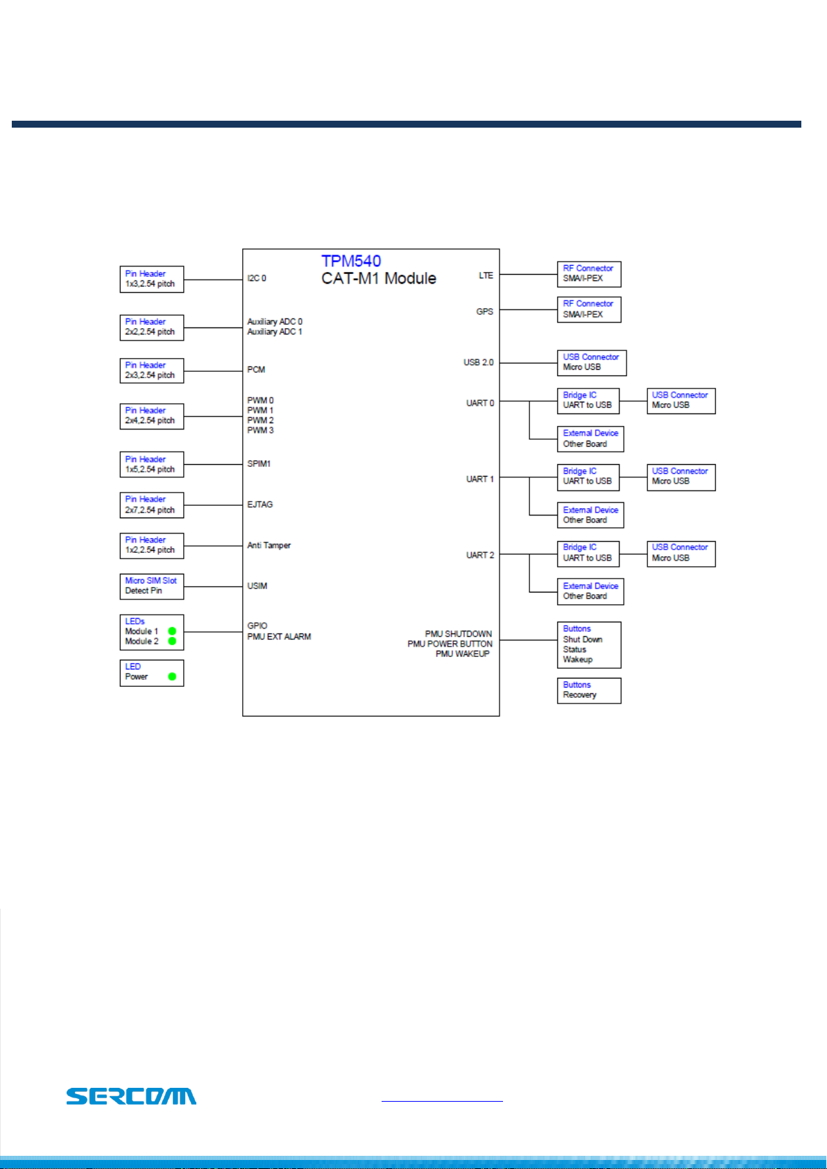
2.1. EVK Block Diagram .............................................................................................................................................. 5
2.2. EVK Interfaces..................................................................................................................................................... 6
3. Starting with TPM540 EVK..................................................................................................................................................... 7
3.1. Hardware preparation and setup .......................................................................................................................... 7
3.2. Software preparation and setup............................................................................................................................ 8
3.3. Starting to access EVK and TPM540....................................................................................................................... 8
4. Button introduce.................................................................................................................................................................. 9
4.1. RECOVERY button:............................................................................................................................................... 9
4.2. WAKEUP button:................................................................................................................................................. 9
4.3. RESET button:..................................................................................................................................................... 9
4.4. STATUS button:................................................................................................................................................... 9
5. LED status ..........................................................................................................................................................................10
5.1. Module_PWR1 LED:............................................................................................................................................10
5.2. Module_LED1: ...................................................................................................................................................10
5.3. Module_LED2: ...................................................................................................................................................10
6. Special hardware configuration pins ......................................................................................................................................11
6.1. SWD(JP17): TBD .................................................................................................................................................11
6.2. Isolation control(JP3): .........................................................................................................................................11
6.3. Debug Selection(JP12): .......................................................................................................................................11
6.4. Anti Tamper(JP11): TBD ......................................................................................................................................11
7. Firmware Upgrade...............................................................................................................................................................12