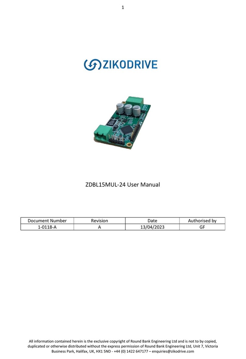
SET SET-1240 Parts list manual

1 of 10
www.smart-e-tech.com
SET-1240
Technical Description
Issue 02 13/04/2022
TECHNICAL DESCRIPTION
SET-1240
8 Channel 4/6-wire xVDT Emulator
This document 9040TDD1100 is a technical description of the SET-1240 xVDT Emulator card.
Note
Before you begin, complete the Software and Hardware installation procedures
applicable to your application.
Note
The guidelines in this document are specific to the SET-1240. The other
components in the system might not meet the same safety ratings. Refer to the
documentation of each component in the system to determine the safety and
EMC ratings for the entire system.
MORE INFORMATION ON OUR WEBSITE:
www.smart-e-tech.de/slsc

2 of 10
www.smart-e-tech.com
SET-1240
Technical Description
Issue 02 13/04/2022
Safety Guidelines
Caution Do not operate the SET-1240 in a manner not specified in this document. Product
misuse can result in a hazard. You can compromise the safety protection built into the product
if the product is damaged in any way. If the product is damaged, return it for repair.
Electromagnetic Compatibility Guidelines
This product was tested and complies with the regulatory requirements and limits for electromagnetic
compatibility (EMC). These requirements and limits provide reasonable protection against harmful
interference when the product is operated in the intended operational electromagnetic environment.
This product is intended for use in industrial locations. However, harmful interference may occur in
some installations, when the product is connected to a peripheral device or test object, or if the
product is used in residential or commercial areas. To minimize interference with radio and television
reception and prevent unacceptable performance degradation, install, and use this product in strict
accordance with the instructions in the product documentation.
Furthermore, any changes or modifications to the product not expressly approved by SET GmbH could
void your authority to operate it under your local regulatory rules.
Caution
To ensure the specified EMC performance, operate this product only with
shielded cables and accessories.
Caution
To ensure the specified EMC performance, the length of any cable attached to
connectors J1 and J2 must be no longer than 3 m (10 ft).

3 of 10
www.smart-e-tech.com
SET-1240
Technical Description
Issue 02 13/04/2022
Description
The SET-1240 xVDT Emulator Card provides 8 independent xVDT emulator channels, with galvanic
isolated I/O. By this the applied excitation voltage and frequency can vary from channel to channel. Each
channel can be configured individually as 6-wire or 4/5-wire xVDT emulation.
The SET-1240 xVDT Emulator Card works with a wide excitation frequency range of 400 Hz to 10 kHz.
The emulated A and B signals can be controlled separately. This allows the SET-1240 xVDT Emulator
Card to emulate resolvers. In 5 and 6 wire configuration this also makes the simulation of over and
undervoltage faults of the A + B current sum signal possible.
The SET-1240 xVDT Emulator Card has several self-test features. One of them allows the use an
excitation signal injected by the instrumentation bus of the RTI, instead of the excitation signals from
the front I/O: The RTI excitation can be used for both, self-test, and normal operation.
The self-test excitation generation circuit of the SET-1240 xVDT Emulator Card can generate a 400 Hz, 1
kHz, and 10 kHz excitation signal. Either this signal or the RTI excitation can be selected as test excitation.
As test CNTL signal 0 V and ±10 V ±2% can be selected, which represents a gain of 0 and 1 ±2%.
Instead of passing the A and B signals to the Front I/O, they can be switched to the internal test bus
(Test_A+, Test_B+ and Test_AB-). The internal test bus can be forwarded either to the Self-test
Evaluation circuit or to the instrumentation bus of the RTI. This includes the selection of either Test_A+
or Test_B+ as Test_AB+ signal.
The transformers used for the galvanic isolation are mounted on an internal sub-card and can be easily
replaced. Please contact the SET sales department if you require a customized transformer module.

5 of 10
www.smart-e-tech.com
SET-1240
Technical Description
Issue 02 13/04/2022
15
30
44
14
29
43
13
28
42
12
27
41
11
26
40
10
25
39
9
24
38
8
23
37
7
22
36
6
21
35 5
20
34
4
J1, J2 Pinout (Front)
J1 J2
Signal
Description
CHx_A+/-
6-wire mode:
Emulated A signal output.
4/5-wire mode:
CHx_A+ to be used as signal output (in 5-wire
applications either CHx_A- or CHx_B+ can be used for
common/GND line).
CHx_B+/-
6-wire mode:
Emulated A signal output.
4/5-wire mode:
CHx_B- to be used as signal output (in 5-wire
applications either CHx_A- or CHx_B+ can be used for
common/GND line).
CHx_EXC+/-
Excitation input
NC
No connection
J1, J2 Connector Pin Assignments
15
30
44
14
29
43
13
28
42
12
27
41
11
26
40
10
25
39
9
24
38
8
23
37
7
22
36
6
21
35
5
20
34
4
19
33
3
18
32
2
17
31
1
16
CH7_A+
CH7_A-
CH6_B+
CH6_B-
CH6_A+
CH6_A-
NC
NC
CH5_A+
CH5_A-
CH4_B+
CH4_B-
CH4_A+
CH4_A-
NC
NC
CH3_A+
CH3_A-
CH2_B+
CH2_B-
CH2_A+
CH2_A-
NC
NC
CH1_A+
CH1_A-
CH0_B+
CH0_B-
CH0_A+
CH0_A-
CH7_B+
CH7_B-
NC
NC
CH5_B+
CH5_B-
NC
NC
CH3_B+
CH3_B-
NC
NC
CH1_B+
CH1_B-
15
30
44
14
29
43
13
28
42
12
27
41
11
26
40
10
25
39
9
24
38
8
23
37
7
22
36
6
21
35
5
20
34
4
19
33
3
18
32
2
17
31
1
16
NC
NC
NC
NC
NC
NC
NC
NC
NC
NC
NC
NC
NC
NC
NC
NC
CH6_EXC+
CH6_EXC-
CH5_EXC+
CH5_EXC-
CH4_EXC+
CH4_EXC-
NC
NC
CH2_EXC+
CH2_EXC-
CH1_EXC+
CH1_EXC-
CH0_EXC+
CH0_EXC-
NC
NC
NC
NC
NC
NC
NC
NC
CH7_EXC+
CH7_EXC-
NC
NC
CH3_EXC+
CH3_EXC-

7 of 10
www.smart-e-tech.com
SET-1240
Technical Description
Issue 02 13/04/2022
Row
e
d
c
b
a
1
CH1_CTRL_B
CH1_CTRL_A
NC
CH0_CTRL_B
CH0_CTRL_A
2
CH3_CTRL_B
CH3_CTRL_A
NC
CH2_CTRL_B
CH2_CTRL_A
3
GND
GND
GND
GND
GND
4
CH5_CTRL_B
CH5_CTRL_A
NC
CH4_CTRL_B
CH4_CTRL_A
5
CH7_CTRL_B
CH7_CTRL_A
NC
CH6_CTRL_B
CH6_CTRL_A
6
GND
GND
GND
GND
GND
7
NC
NC
NC
NC
NC
8
NC
NC
NC
NC
NC
9
GND
GND
GND
GND
GND
10
NC
NC
NC
NC
NC
11
NC
NC
NC
NC
NC
12
NC
NC
NC
NC
NC
13
NC
NC
NC
NC
NC
14
NC
NC
NC
NC
NC
15
NC
NC
NC
NC
NC
16
NC
NC
NC
NC
NC
17
GND
GND
GND
GND
GND
18
NC
NC
NC
NC
NC
19
NC
NC
NC
NC
NC
20
GND
GND
GND
GND
GND
21
NC
NC
NC
NC
NC
22
NC
NC
NC
NC
NC
23
GND
GND
GND
GND
GND
24
NC
NC
NC
NC
NC
25
NC
NC
NC
NC
NC
XJ2 Connector Pin Assignments
Signal
Description
CHx_CNTL_A
Controls the A signal generation
CHx_CNTL_B
Controls the B signal generation
GND
Ground connection
NC
No connection
XJ2 Connector Signal Descriptions

8 of 10
www.smart-e-tech.com
SET-1240
Technical Description
Issue 02 13/04/2022
XJ3 Connector Pinout (Rear)
Pins
Signal
Slot1/Slot2
H
V1+
Instrument 0+
G
V1-
Instrument 0-
F
V2+
Instrument 1+
E
V2-
Instrument 1-
D
V3+
NC
C
V3-
NC
B
V4+
NC
A
V4-
NC
XJ3 Connector Pin Assignments
Signal
Description
Instrument 0+
Input: RTI Excitation +
Instrument 0-
Input: RTI Excitation -
Instrument 1+
Output: Test Signal AB+
Instrument 1-
Output: Test Signal AB-
NC
No connection
XJ3 Connector Signal Descriptions
H
G
F
E
D
C
B
A

9 of 10
www.smart-e-tech.com
SET-1240
Technical Description
Issue 02 13/04/2022
LED Behavior
LED Name
LED Behavior
Definition of Behavior
PWR
Off
No power present on the board
Solid green
Power good state
RDY
Off
Module card is unpowered or reset active
Solid green
Card is recognized by chassis and ready to communicate
Amber
Chassis is communicating
Error Handling
LED Name
LED Behavior
Actions
PWR
Off
-Check power supply of chassis
-Check external power supply if used
PWR
Blinking Red
-Check plugin module on board
-Check fuse on board
Hardware Specifications
Absolute Maximum Ratings
Property
Condition
Value
Comment
Max. Excitation Voltage
Recommended
Operation Range
400 Hz ≤ fExc ≤ 1 kHz: 3 VRMS
1 kHz < fExc ≤ 10 kHz: 7 VRMS
Operation without
damage
10 VRMS
Max. Common mode
Excitation Voltage
45 VDC
Min. Common mode
Excitation Voltage
-45 VDC
Max. RTI CNTL Voltage
+10 V
Min. RTI CNTL Voltage
-10 V
Excitation Frequency
Recommended
Operation Range
400 Hz –10 kHz

10 of 10
www.smart-e-tech.com
SET-1240
Technical Description
Issue 02 13/04/2022
Technical Data
Property
Condition
Value
Comment
Update Time
10 ms
SLSC Commit
CMD duration
Expected Electrical
Relay Lifetime
1 A, 30 VDC resistive
10ˆ5 operations
DC Resistance of
Transformers
115 Ω ±15%
Physicals Characteristics
Property
Condition
Value
Comment
Module Dimensions
Excluding ejector
144.32 mm x 30.48 mm
x 302 mm (H x W x D)
Standard SLSC card size
Front Panel Connector
2x female DB -44 high-
density D-Sub with 4-40
UNC screw lock
For mating connectors
and cables, see below
RTI Connector
2 mm hard metric per
IEC 61076-101
Any RTI marked
Environmental
Property
Condition
Value
Comment
Operating Humidity
Relative, non-
condensing
10%-90%
Storage Humidity
Relative, non-
condensing
5%-95%
Operating Temperature
Forced-air cooling from
chassis
0°C-40°C
Storage Temperature
-40°C-85°C
Maximum Altitude
2000m
Table of contents


