Sharp CD-PC1881V User manual

– 1 –
CD-PC1881V
No. S0961CDPC1881
CD-PC1881V
• In the interests of user-safety the set should be restored to its
original condition and only parts identical to those specified be
used.
SERVICE MANUAL
This document has been published to be used
for after sales service only.
The contents are subject to change without notice.
SHARP CORPORATION
CD-PC1881V Video CD Mini System consisting of CD-PC1881V
(main unit), CP-C881 (front speakers), CP-SW881 (sub woofer),
GBOXS0026AWM1 (center speaker) and GBOXS0027AWM1
(surround speakers).
CONTENTS Page
SAFETY PRECAUTION FOR SERVICE MANUAL ........................................................................................................... 2
VOLTAGE SELECTION..................................................................................................................................................... 2
AC POWER SUPPLY CORD AND AC PLUG ADAPTOR ................................................................................................. 2
SPECIFICATIONS ..............................................................................................................................................................3
NAMES OF PARTS ........................................................................................................................................................... 4
OPERATION MANUAL ...................................................................................................................................................... 7
DISASSEMBLY.................................................................................................................................................................. 8
REMOVING AND REINSTALLING THE MAIN PARTS................................................................................................... 11
ADJUSTMENT ................................................................................................................................................................. 12
BLOCK DIAGRAM ........................................................................................................................................................... 15
SCHEMATIC DIAGRAM .................................................................................................................................................. 18
VOLTAGE ........................................................................................................................................................................ 30
WIRING SIDE OF P.W.BOARD....................................................................................................................................... 31
NOTES ON SCHEMATIC DIAGRAM .............................................................................................................................. 38
TYPES OF TRANSISTOR AND LED............................................................................................................................... 38
WAVEFORMS OF CD CIRCUIT...................................................................................................................................... 39
TROUBLESHOOTING (CD SECTION) ........................................................................................................................... 40
FUNCTION TABLE OF IC................................................................................................................................................ 44
FL SEGMENT ...................................................................................................................................................................56
PARTS GUIDE/EXPLODED VIEW
NTSC/PAL
Manufacturedunderlicensefrom DolbyLaboratories Licensing
Corporation.
DOLBY, the double-D symbol and “PRO LOGIC” are
trademarks of Dolb
y
Laboratories Licensin
g
Corporation.

CD-PC1881V
– 2 –
SAFETY PRECAUTION FOR SERVICE MANUAL
Precaution to be taken when replacing and servicing the Laser Pickup.
The AEL (Accessible Emission Level) of Laser Power Output for this model is specified to be lower than Class I Requirements.
However, the following precautions must be observed during servicing to protect your eyes against exposure to the Laser beam.
(1) When the cabinet has been removed, the power is turned on without a compact disc, and the Pickup is on a position outer than
the lead-in position, the Laser will light for several seconds to detect a disc. Do not look into the Pickup Lens.
(2) TheLaserPowerOutputofthePickupinsidetheunitandreplacementservicepartshavealreadybeenadjustedpriortoshipping.
(3) No adjustment to the Laser Power should be attempted when replacing or servicing the Pickup.
(4) Under no circumstances look directly into the Pickup Lens at any time.
(5) CAUTION - Use of controls or adjustments, or performance of procedures other than those specified herein may result in
hazardous radiation exposure.
VOLTAGE SELECTION
The voltage selector is located on the AC voltage selector box. If adjustment is necessary, use a screwdriver in order to turn the
selector in either direction unitil the correct voltage figure is displayed in the window next the adjustment screw.
QACCA0001AW00
Figure 2 AC POWER SUPPLY CORD AND AC PLUG ADAPTOR
QACCB0006AW00
QACCE0008AW00
QACCJ0003AW00
QACCL0005AW00
This Video CD Mini System is classified as a CLASS 1
LASER product.
The CLASS 1 LASER PRODUCT label is located on the
rear cover.
Useof controls, adjustments or performance ofprocedures
other than those specified herein may result in hazardous
radiation exposure.
As the laser beam used in this compact disc player is
harmful to the eyes, do not attempt to disassemble the
cabinet. Refer servicing to qualified personnel only.
CAUTION Laser Diode Properties
Material: GaAIAs
Wavelength: 780 nm
Emission Duration: continuous
Laser Output: max. 0.6 mW
CAUTION-INVISIBLE LASER RADIATION WHEN OPEN. DO NOT STARE INTO
BEAM OR VIEW DIRECTLY WITH OPTICAL INSTRUMENTS.
VARNING-OSYNLIG LASERSTRALNING NAR DENNA DEL AR OPPNAD. STIRRA
EJ IN I STRALEN OCH BETRAKTA EJ STRALEN MED OPTISKA INSTRUMENT.
ADVERSEL-USYNLIG LASERSTRALING VED ABNING. SE IKKE IND I
STRALEN-HELLER IKKE MED OPTISKE INSTRUMENTER.
VARO! AVATTAESSA OLET ALTTIINA NAKYMATON LASERSATEILYLLE.
ALA TUIJOTA SATEESEEN ALAKA KATSO SITA OPTISEN LAITTEEN LAPI.
VARNING-OSYNLIG LASERSTRALNING NAR DENNA DEL AR OPPNAD.
STIRRA EJ IN I STRALEN OCH BETRAKTA EJ STRALEN GENOM OPTISKT
INSTRUMENT.
ADVERSEL-USYNLIG LASERSTRALING NAR DEKSEL APNES. STIRR IKKE
INN I STRALEN ELLER SE DIREKTE MED OPTISKE INSTRUMENTER.
QPLGA0003AWZZ QPLGA0004AWZZ

– 3 –
CD-PC1881V
Specifications for this model are subject to change without
prior notice.
SPECIFICATIONS
CD-PC1881V
CP-C881
FOR A COMPLETE DESCRIPTION OF THE OPERATION OF THIS UNIT, PLEASE REFER
TO THE OPERATION MANUAL.
GBOXS0026AWM1
GBOXS0027AWM1
CP-SW881
General
Power source: AC110/127/220/230-240V,50/60 Hz
Power consumption: 140 W
Dimensions: Width; 270 mm (10-5/8")
Height; 300 mm (11-13/16")
Depth; 362 mm (14-1/4")
Weight: 8.1 kg (17.7 lbs.)
Amplifier section
Output power: Front speakers;
MPO; 176 W(88 W + 88 W)
(10 % T.H.D.)
RMS; 80 W (40 W + 40 W)
(10 % T.H.D.)
RMS; 72 W (36 W + 36 W)
(0.9 % T.H.D.)
Center speaker;
MPO; 32 W (10 % T.H.D.)
RMS; 20 W (10 % T.H.D)
RMS; 14 W (0.9 % T.H.D)
Surround speakers;
MPO; 32 W (16 W + 16 W)
(10 % T.H.D.)
RMS; 20 W (10 W + 10 W)
(10 % T.H.D.)
RMS; 14 W (7 W + 7 W)
(0.9 % T.H.D.)
Sub woofer;
MPO; 72 W (10 % T.H.D.)
RMS; 40 W (10 % T.H.D)
RMS; 32 W (0.9 % T.H.D)
Output terminals: Front speakers; 6 ohms
Centre speaker; 4 ohms
Surround speakers; 8 ohms
Sub woofer; 6 ohms
Headphones; 16-50 ohms
(recommended; 32 ohms)
Video out; 1 Vp-p (75 ohms)
Input terminals: Video/Auxiliary (audio signal) x 2;
500 mV/47 kohms
Compact disc player section
Type: 3-discmulti-play compactdisc player
Signal readout: Non-contact,3-beamsemi-conductor
laser pickup
D/A converter: 1-bit D/A converter Frequency
Frequency
response: 20 - 20,000 Hz
Dynamic range: 90 dB (1 kHz)
Video CD section
Video output format: PAL/PAL60/NTSC
Tuner section
Frequency range: FM; 88-108 MHz
AM; 531-1,602 kHz
Cassette deck section
Frequency response: 50-14,000 Hz (Normal tape)
Signal/noise ratio: 55 dB (TAPE 1, playback)
50 dB (TAPE 2, recording/
playback)
Wow and flutter: 0.15 % (WRMS)
Front speaker section
Type: 3-way type [13 cm (5-1/4") woofer,
5 cm (2") tweeter and super tweeter]
Maximum input power: 80 W
Rated input power: 40 W
Impedance: 6 ohms
Dimensions: Width; 200 mm (7-7/8")
Height; 300 mm (11-13/16")
Depth; 254 mm (10")
Weight: 2.9 kg (6.3 lbs.)/each
Center speaker section
Type: 10 cm (4") full-range speaker
Maximum input power: 40 W
Rated input power: 20 W
Impedance: 4 ohms
Dimensions: Width; 260 mm (10-1/4")
Height; 140 mm (5-1/2")
Depth; 155 mm (6-1/8")
Weight: 0.9 kg (2.0 lbs.)
Surround speaker section
Type: 10 cm (4") full-range speaker
Maximum input power: 20 W
Rated input power: 10 W
Impedance: 8 ohms
Dimensions: Width; 170 mm (6-3/4")
Height; 88 mm (3-1/2")
Depth; 170 mm (6-3/4")
Weight: 0.5 kg (1.0 lbs.)/each
Sub woofer section
Type: 13 cm (5-1/4") full-range speaker
Maximum input power: 80 W
Rated input power: 40 W
Impedance: 6 ohms
Dimensions: Width; 200 mm (7-7/8")
Height; 300 mm (11-13/16")
Depth; 310 mm (12-3/8")
Wei
g
ht: 3.4 k
g
(
7.5 lbs.
)

CD-PC1881V
– 4 –
NAMES OF PARTS
CD-PC1881V
■ Front panel
1. Disc Number Selector Buttons
2. Disc Tray
3. Multi Indicator
4. Disc Skip Button
5. Open/Close Button
6. Dolby Pro Logic Indicator
7. Extra Bass Indicator
8. FM Stereo Mode Indicator
9. FM Stereo Indicator
10. (VCD/CD) Play Indicator
11. (VCD/CD) Pause Indicator
12. (VCD/CD) Repeat Indicator
13. (VCD/CD) Disc Number Indicators
14. (VCD/CD/TUNER) Memory Indicator
15. Timer Play Indicator
16. Timer Record Indicator
17. Spectrum Analyzer/Volume Level Indicator
18. (TAPE 2) Record Indicator
19. Sleep Indicator
20. Timer Set Indicator
21. (VCD) Digest Button
22. (VCD) Book Mark Button
23. (VCD) Skip Previous Button
(CD) Track Down/Review Button
(TUNER) Preset Down Button
(TAPE 2) Rewind Button
24. (VCD) Skip Next Button
(CD) Track Up/Cue Button
(TUNER) Preset Up Button
(TAPE 2) Fast Forward Button
25. Bypass Button
26. Normal Button
27. Timer/Sleep Button
28. Clock Button
29. (VCD) Playback Control Auto/Off Button
30. (VCD/CD) Audio Mode Button
31. (VCD) On Screen Display On/Off Button
32. On/Stand-by Button
33. Equalizer Mode Selector Button
34. Dimmer Button
35. Phantom Button
36. Extra Bass/Demo Mode Button
37. Volume Control
38. Headphone Socket
39. Function Selector Button
40. (TAPE 2) Record Pause Button
41. Memory/Set Button
42. (VCD) Stop/Return
(CD/TAPE) Stop Button
43. (VCD) Play/Repeat/Select/Resume Button
(CD) Play/Repeat Button
(TAPE) Play Button
44. Tuning and Time Up/Down Buttons
45. Sub Woofer Volume Control
46. (TAPE 1) Cassette Compartment
47.
(
TAPE 2
)
Cassette Com
p
artment
123 45
6
12
17 18 19
7
8
910
13
14
15
16
11
46 47
20
3839 40 41 42 43 44 45
27 33
34
35
36
37
28
29
30
31
32
212223 242526
123 45

– 5 –
CD-PC1881V
CP-C881
GBOXS0026AWM1
GBOXS0027AWM1
7891011
1
2
3
4
5
6
1
2
3
45
6
7
8
9
10
11
12
CP-SW881
■ Rear panel
1. Video Output Socket
2. AC Power Lead
3. AM Aerial Terminal
4. Aerial Earth Terminal
5. FM 75 Ohms Aerial Terminal
6. Video/Auxiliary (Audio Signal) Input Sockets
7. AC Voltage Selector
8. Surround Speaker Terminals
9. Centre Speaker Terminals
10. Front Speaker Terminals
11. Sub Woofer Terminals
■ Front speaker
1. Super Tweeter
2. Tweeter
3. Woofer
4. Bass Reflex Duct
5. Speaker Wire
■ Center speaker
6. Full-Range Speaker
7. Speaker Wire
■ Surround speaker
8. Full-Range Speaker
9. Speaker Wire
■ Sub woofer
10. Woofer
11. Bass Reflex Duct
12. S
p
eaker Wire

CD-PC1881V
– 6 –
■ Remote control
1. Remote Control Transmitter LED
2. On/Stand-by Button
3. Surround Level Buttons
4. Centre Level Buttons
5. Dolby Pro Logic Button
6. Centre Mode Button
7. Test Tone Button
8. (VCD/CD) Direct Search Buttons
9. (VCD) On Screen Display On/Off Button
10. (VCD) PAL/NTSC Select Button
11. (VCD) Book Mark Button
12. (VCD) Digest/Time Search Button
13. (VCD/CD) Audio Mode Button
14. (VCD) VCD Auto/On Button
15. (VCD) Playback Control Auto/Off Button
16. (VCD/CD) Clear Button
17. (VCD/CD) Memory Button
18. (VCD/CD) Disc Skip Button
19. (VCD/CD) Random Button
20. (VCD/CD) Pause Button
21. (TAPE 2) Record Pause Button
22. (VCD) Skip/Previous Button
(CD) Track Down/Review Button
(TUNER) Preset Down Button
(TAPE 2) Rewind Button
23. (VCD) Skip/Next Button
(CD) Track Up/Cue Button
(TUNER) Preset Up Button
(TAPE 2) Fast Forward Button
24. (VCD) Stop/Return Button
(CD/TAPE) Stop Button
25. (VCD) Play/Repeat/Select/Resume Button
(CD) Play/Repeat Button
(TAPE) Play Button
26. Function Selector Buttons
27. Extra Bass Button
28. Equalizer Mode Button
29. Balance Control Buttons
30. Volume Up/Down Buttons
6
8
5
4
3
12
19
12
11
10
9
29
28
27
26
7
14
13
15
16
17
30
1821 20
24 2522 23

– 7 –
CD-PC1881V
OPERATION MANUAL
Notes concerning use:
Replace the batteries if the operating distance is reduced or
if the operation becomes erratic.
Periodicallycleanthetransmitter LED on theremotecontrol
and the sensor on the main unit with a soft cloth.
Exposing the sensor on the main unit to strong light may
interfere with operation. Change the lighting or the direction
of the unit.
Keeptheremote controlaway frommoisture,excessive heat,
shock, and vibrations.
■Remote control
0.2 m - 6 m
(8" - 20')
15
15
Reset the microcomputer under the following con-
ditions:
To erase all of the stored memory contents (clock and timer
settings, and tuner and CD presets).
If the display is not correct.
If the operation is not correct.
1
Pressthe ON/STAND-BY buttontoenter thestand-by mode.
2
Whilst pressing down the button and the button,
hold down the ON/STAND-BY button for at least 1 second.
Caution:
The operation explained above will erase all data stored in
memory including clock and timer settings, and tuner, video
CD and CD presets.
ON/
STAND-BY
RESETTING THE MICROCOMPUTER
SETTING THE CLOCK
(Main unit operation)
TUNING/
TIME
( )
MEMORY/
SET
CLOCK
ON/
STAND-BY
7
Press the MEMORY/SET button.
8
Press the TUNING/TIME ( or ) button to adjust the
minutes.
Press the TUNING/TIME ( or ) button once to advance
the time by 1 minute. Hold it down to change the time in 5
minute intervals.
The hour setting will not advance even if minutes advance
from “59” to “00”.
9
Press the MEMORY/SET button.
The clock starts operating from “0” seconds.
(Seconds are not displayed.)
And then the clock display will disappear a few seconds.
To see the time display:
Press the CLOCK button.
The time display will appear for about 5 seconds.
Note:
The clock display will flash on and off at the push of the
CLOCK button when the AC power supply is restored after
a power failure occurs or after theAC power lead is discon-
nected.
If this happens, follow the procedure below to change the
clock time.
To change the clock time:
①
Press the CLOCK button.
➁
Within 5 seconds, press the MEMORY/SET button.
➂
Perform steps 6 - 9 above.
To change the time display mode:
①
Perform steps 1 - 2 in the section “RESETTING THE MI-
CROCOMPUTER”, .
➁
Perform steps 1 - 9 above.
In this example, the clock is set for the 24-hour (0:00) system.
1
PresstheON/STAND-BYbuttonto enter thestand-bymode.
2
Press the CLOCK button.
3
Within 5 seconds, press the MEMORY/SET button.
4
Press the TUNING/TIME ( or ) button to select the time
display mode.
AM 12:00AM 0:000:00
Press the TUNING/TIME ( or ) button once to advance
the time by 1 hour. Hold it down to advance continuously.
When the 12-hour display is selected, “AM” will change au-
tomatically to “PM”.
“0:00” →The 24-hour display will appear.
(0:00 - 23:59)
“AM 0:00” →The 12-hour display will appear.
(AM or PM 0:00 - 11:59)
“AM 12:00” →The 12-hour display will appear.
(AM or PM 12:00 - 11:59)
Note that this can only be set when the unit is first installed
or it has been reset.
5
Press the MEMORY/SET button.
6
PresstheTUNING/TIME ( or ) button to adjust the hour.

CD-PC1881V
– 8 –
DISASSEMBLY
Caution on Disassembly
Follow the below-mentioned notes when disassembling
the unit and reassembling it, to keep it safe and ensure
excellent performance:
1. Take cassette tape and compact disc out of the unit.
2. Be sure to remove the power supply plug from the wall
outlet before starting to disassemble the unit.
3.Take off nylonbands orwire holders where they needto
beremovedwhendisassemblingtheunit.Afterservicing
theunit, be sureto rearrangethe leads wherethey were
before disassembling.
4. Take sufficient care on static electricity of integrated
circuits and other circuits when servicing.
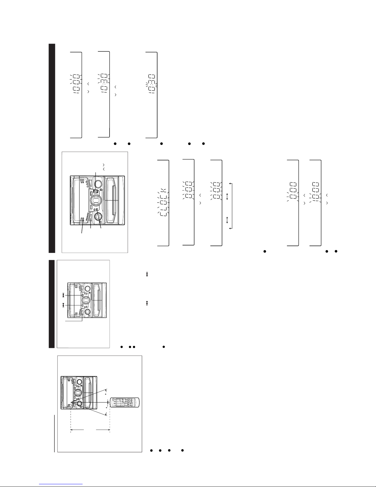
Figure 8-2
Figure 8-3
CD-PC1881V
1 Top Cabinet 1. Screw ..................... (A1) x4 8-1
2 Side Panel 1. Screw ..................... (B1) x4 8-1
(Left/Right) 2. Screw ..................... (B2) x2
3 CD Tray Cover/ 1. Turn on the power supply, 8-2
CD Player Unit open the disc tray, take out
the CD cover, and close.
(Note 1) (Note 2)
2. Hook....................... (C1) x5
3. Hook....................... (C2) x2
4. Socket .................... (C3) x4
5. Screw ..................... (C4) x2
4 Jack PWB 1. Screw ..................... (D1) x1 8-2
5 Rear Panel 1. Screw ..................... (E1) x2 8-2
2. Screw ..................... (E2) x8
3. Screw ..................... (E3) x2
4. Socket .................... (E4) x1
6 Tuner PWB 1. Screw ..................... (F1) x1 8-2
2. Socket .................... (F2) x1
7 Main PWB 1. Socket .................... (G1) x2 9-1
2. Flat Cable .............. (G2) x1
3. Flat Wire................. (G3) x1
4. Tip Wire.................. (G4) x1
5. Screw ..................... (G5) x1
6. Socket .................... (G6) x1
8 Power PWB 1. Screw ..................... (H1) x4 9-1
2. Screw ..................... (H2) x2
3. Socket .................... (H3) x4
4. PWB Holder ........... (H4) x4
9 Front Panel 1. Screw ..................... (J1) x1 9-2
2. Screw ..................... (J2) x2
10 Display PWB/ 1. Screw ..................... (K1) x13 9-2
Switch PWB
2.
Bracket Support ..... (K2) x1
Headphones PWB 3.
Knob ....................... (K3) x1
11 Tape Mechanism 1. Open the cassette holder. 9-2
2. Screw...................... (L1) x6
3. Socket .................... (L2) x1
12 Turntable 1. Screw ..................... (M1) x1 9-3
2. Cover ..................... (M2) x1
13 Disc Tray 1. Screw ..................... (N1) x2 9-3
2. Guide ..................... (N2) x2
14 CD Video PWB 1. Screw ..................... (P1) x1 9-4
2. Socket .................... (P2) x4
15 CD Changer 1. Screw ..................... (Q1) x4 9-5
Mechanism
16 CD Mechanism 1. Screw ..................... (R1) x1 9-5
STEP R EMOVAL PROCEDURE FIGURE Figure 8-1
LOCK
LEVER
Note 1:
How to open the changer manually. (Fig. 8-3)
1. Change, turn fully the lock lever in the arrow direction
throughtheholeontheloadingchassisbottominthisstate.
After that, push forward the CD player base.
Note 2:
1.After removingthe connectorfor theoptical pickupfrom the
connector, wrap the conductive aluminium foil around the
front end of connector to protect the optical pickup from
electrostatic damage.
Top Cabinet
(A1)x2
ø3x12mm
(A1)x2
ø3x12mm
Side Panel (Left) (B1)x2
ø3x8mm
(B1)x2
ø3x8mm
(B2)x2
ø3x10mm
Rear Panel
Side Panel
(Right)
Front Panel
(E2)x8
ø3x10mm
(E4)x1
(F2)x1
(E1)x2
ø3x10mm
Rear Panel
CD Tray
Cover
Main PWB
CD Player
Unit
Hook
(C1) x5
(C2) x1
(C4) x1
ø3x10mm
(C4) x1
ø3x10mm
(C3) x4
1
1
2
Pull
(C2) x1
CD Video PWB
(F1) x1
ø3x10mm
(D1) x1
ø3x10mm
Jack PWB Front Panel
(E3)x2
ø3x10mm
Tuner PWB
DiscTray

– 9 –
CD-PC1881V
Figure 9-1
Figure 9-2
Figure 9-3
Be careful when installing the CD changer mechanism.
InstalltheCDchangermechanismontheCDplayerbaseafter
the shift lever has been set in the highest position.
Figure 9-4
Figure 9-5
(H1)x4
ø3x10mm
(G1)x2
(H4)x4
(G2)x1
Front Panel
(H3)x2
(H3)x2
(G5)x1
ø3x10mm
Push Push
1 1
2Pull
POWER
PWB
Main PWB
Power PWB
(G3)x1
Headphoens
PWB
(G6)x1
Display PWB
(G4)x1
(H2)x2
ø3x6mm
Front Panel
Display PWB
(K2)x1
Switch PWB
Open
Cassette
Holder
(Left/Right)
Tape
Mechanism
(K1)x2
ø3x10mm
(K1)x10
ø3x10mm
(K1)x1
ø3x10mm
(L1)x6
ø3x10mm (J2)x2
ø3x8mm
(J1)x1
ø3x10mm
Headphones
PWB
(L2)x1
(K3)x1
Main Chassis
(N1) x1
ø3 x10mm
(N1) x1
ø3 x10mm
(M1) x1
ø3 x10mm
Turntable
Disc Tray
(M2) x1
(N2) x1
(N2) x1
CD Player Unit
Washer
(P1) x1
ø3 x10mm
(P2) x2
(P2) x2 CD Player Unit
CD Video PWB
(Q1) x4
ø3 x12mm
(R1) x1
ø2.6 x10mm
CD Changer
Mechanism
CD Mechanism
Shift Lever
CD Player Base

CD-PC1881V
– 10 –
Figure 10-2
CP-C881
1 Front Speaker 1. Front Panel ............ (A1) x1 10-1
2. Tip .......................... (A2) x2
3. Screw ..................... (A3) x2
4. Screw ..................... (A4) x2
5. Screw ..................... (A5) x4
STEP REMOVAL PROCEDURE FIGURE
Figure 10-1
CP-SW881
1 Sub woofer 1. Net.......................... (A1) x1 10-2
2. Screw ..................... (A2) x4
STEP REMOVAL PROCEDURE FIGURE
Note:
The surround speakers and center speaker can be
easily disassembled.
Therefore the disassembling method is not described.
For details refer to the disassembling drawing in the
Parts Guide.
(A4)x2
ø3x10mm
(A3)x2
ø3x10mm
Front Panel
(A1)x1 Screw Driver
Woofer
Tweeter
Super
Tweeter
(A5)x4
ø4x14mm
(A2)x2
Speaker Box
Drive should be pried
away from Speaker Box.
(A2)x4
ø4x14mm
Screw
driver Drive should be pried
away from Speaker Box.
Direction of handle
Woofer
Speaker
Box
(A1)x1

– 11 –
CD-PC1881V
How to remove the pickup (See Fig. 11-2)
1.Removethescrews (B1) x2pcs.,toremove theshaft(B2)x
1 pc.
2. Remove the stop washer (B3) x 1 pc., to remove the gear
(B4)x 1 pc.
3. Remove the pickup.
Figure 11-2
REMOVING AND REINSTALLING THE MAIN PARTS
CD MECHANISM SECTION
Performsteps 1,2, 3and 14-16of thedisassembly methodto
remove the CD mechanism.
How to remove the T/T up/down loading motor
(See Fig. 11-1)
1. Remove the screws (A1) x 2 pcs., to remove the T/T up/
down loading motor.
Figure 11-1
Note
After removing the connector for the optical pickup from the
connector, wrap the conductive aluminium foil around the
front end of connector to protect the optical pickup from
electrostatic damage.
(B1) x2
ø2.6 x6mm
Shaft
(B2) x1
Stop Washer
(B3) x1
Gear
(B4) x1
CD Mechanism
Pickup
(A1) x2
ø2.6 x5mm
T/T Up/Down
Loading Motor
Motor
PWB

CD-PC1881V
– 12 –
• AM IF/RF
Signal generator: 400 Hz, 30%, AM modulated
*1. Input: Antenna, Output: TP302
*2. Input: Antenna, Output: TP301
TUNER SECTION
fL: Low-range frequency
fH: High-renge frequency
AM IF 450 kHz 1,602 kHz T351 *1
AM Band — 531 kHz (fL): T306 *2
Coverage 1.1 ±0.1 V
AM Tracking 990 kHz 990 kHz (fH): T302 *1
Test Stage Frequency Frequency
Display Setting/
Adjusting
Parts
Instrument
Connection
Figure 12-2 ADJUSTMENT POINTS
CD ERROR CODE DESCRIPTION
When a malfunction occurs during CD operation, an error
code will be displayed to identify the function in CD operation
which failed.
Error State Code
0001 Cannot detect pickup-in SW
0101 Tray close operation error
0105 Tray close operation error
0201 Tray open operation error
0203 Tray open operation error
0304 Disc skip operation error
0305 Disc skip operation error
0307 Disc skip operation error
• FM
Notes:
1: Description of the "FM IF Adjustment" is not carried on this
Manual. It is because the IF coil in the FM front end section
has been best adjusted in the factory so that its further
adjustment is not needed at the field. When replacing the
FM front end assembly, no adjustment is needed either.
2: The parts in the FM front end section are prepared in a
complete unit, so you can't obtain each part individually.
Adjusting
Parts Instrument
Connection
Frequency
Display
Frequency
• FM Mute Level
Signal generator: 1 kHz, 40 kHz dev., FM modulated
98.00 MHz 98.00 MHz VR351 Input: Antenna
(25 dBµV) Output: Speaker
Terminal
MECHANISM SECTION
•Driving Force Check
Torque Meter Specified Value
Play: TW-2412 Tape 1: Over 80 g
Tape 2: Over 80 g
•Torque Check
Torque Meter
Tape 2
Play: TW-2111 30 to 60 g. cm 30 to 60 g.cm
Fast forward: TW-2231 — 60 to 120 g.cm
Rewind: TW-2231 — 60 to 120 g.cm
Specified
Value
Adjusting
Point Instrument
Connection
Test Tape
Normal MTT-111 Variable 3,000 ±Speaker
speed Resistor in 30 Hz terminal
motor. (Load
(MM1) resistance:
8 ohms)
ADJUSTMENT
Specified Value
Tape 1
•Tape Speed
Figure 12-1
TAPE MECHANISM
MM 1
Motor
Variable Resistor in motor
TP302
R357
T351 VR351
FM MUTE
LEVEL
R336 TP301
FE301
IC303 T306
T302
SO301
ANTENNA
TERMINAL
TUNER PWB
AM IF
AM BAND
COVERAGE fL
AM
TRACKING fH

– 13 –
CD-PC1881V
TEST MODE
Figure 13-2 Figure 13-3
Since this CD system incorporates the following automatic adjustment function, when the pickup is replaced, it is not necessary
to readjust it.
Since this CD unit does not need adjustment, the combination of PWB and laser pickup unit is not restricted.
• Automatic adjustment item
1. Focus offset (Fig. 13-2)
2. Tracking offset (Fig. 13-3)
3. E/F balance (tracking error balance) (Fig. 13-4)
4. RF level AGC function (HF level: constant)
5. RF level automatic follow-up of the tracking gain
This automatic adjustment is performed each time a disc is changed. Therefore,
each disc is played back using the optimal settings.
CD SECTION Figure 13-1
Note:
Only in STOP state it is possible to slide the pickup with the ( ) or ( ) key.
VOL. --- Last memory
BAL. --- CENTER
R.GEQ. --- FLAT
X-BAS --- OFF
Canceling method - POWER OFF
• Setting the test mode
Any one of test mode can be set by pressing several keys as follows.
<CD> + < > + <POWER> TEST: CD operation test
• TEST mode
Function — CD test mode
Setting of TEST mode
Indication of CD TST mode (Fig. 13-1)
OPEN/CLOSE operation is manual operation.
The pickup can be moved by using the ( ) or ( ) key.
<MEMORY>
LASER ON
<PLAY> key input Press <STOP> key. Stop
TOC. IL is performed, and the ordinary PLAY is performed.
If the following key is pressed during PLAY, it is possible
to specify directly any Track No.
<Disc Number 1> key: Track 4
<Disc Number 2> key: Track 9
<Disc Number 3> key: Track 15
<MEMORY>
Tracking on the spot.
SERVO OFF PLAY
<MEMORY>
Tracking on the spot.
SERVO ON PLAY STOP
Figure 13-4
IL is not performed.
<STOP>
1 2 3
2
0.1s
0.50 V
IC1 20 FE
0.1s
0.50 V
IC1 7 TE
1
FOCUS
OFF-SET
ADJUST
TRACKING
OFF-SET
ADJUST
2
1
10ms
0.50 V
IC1 20 FE
10ms
0.50 V
IC1 7 TE
Enlarged
View
TRACKING
OFF-SET
ADJUST
2
1
TO
TE
200 ms
1V/diV
IC 1 15
200 ms
1V/diV
IC 1 7
TRACKING/
ERROR
BARANCE
ADJUST

CD-PC1881V
– 14 –
SP out L-ch Input signal is output.
(SO901) R-ch Input signal is output.
(SO901) SP out C-ch SP cut, no output
(SO901) SP out S-ch
Almost no output (only omitting component)
SP out L-ch Almost no output (only omitting component)
(SO901) R-ch Almost no output (only omitting component)
(SO901) SP out C-ch
Input signal is output.
(SO901) SP out S-ch
Almost no output (only omitting component)
State of set Dolby Pro Logic Dolby Pro Logic On mode
Output point Bypass mode Normal mode Phantom mode
IC501 12 pin L-out Output enabled state Output enabled state Output enabled state
11 pin R-out Output enabled state Output enabled state Output enabled state
IC501 9pin C-out No output Output enabled state No output
IC501 10pin S-out No output Output enabled state Output enabled state
SP OUT L-ch Output enabled state Output enabled state Output enabled state
(SO901) R-ch Output enabled state Output enabled state Output enabled state
SP OUT C-ch No output in MUTE (Q404) state Output enabled state No output in MUTE (Q404) state
(SO901)
SP OUT S-ch No output in MUTE (Q403) state Output enabled state Output enabled state
(SO901)
EXPLANATION OF DOLBY SURROUND PRO LOGIC AND EVALUATION METHOD
Test tone output
• Pro Logic ON Normal mode
Press the remote control TEST TONE button.
→Output of only L-ch →Output of only C-ch
↑ ↓
Output of only S-ch ←Output of only R-ch
The test tone (noise) is repeatedly output for output period
(2 sec).
In this case the following indication appears repeatedly.
→TEST →L-ch →C-ch
↑ ↓
S-ch ← R-ch
• Pro Logic ON Phantom mode
Press the remote control TEST TONE button.
→Output of only L-ch →Output of only R-ch
↑ ↓
←Output of only S-ch
The test tone (noise) is repeatedly output for output period
(2 sec).
In this case the following indication appears repeatedly.
→TEST → L-ch → R-ch
↑↓
←S-ch←
Outline
• Namely, two speakers are connected in parallel to one
amplifier.
•IntheProLogicBYPASSmodetheamplifierforC-ch(center
channel)andtheamplifierforS-ch(surroundchannel)arein
MUTE state. The SP output is cut.
• In the normal mode of Pro Logic ON mode the amplifiers for
C-ch and S-ch are in operative state, so that the SP output
appears.
•Inthe Phantommode ofProLogic ONmode theamplifierfor
C-ch is in MUTE state, so that the SP output is cut. The
amplifierfor S-ch (surround) isin operative state, sothat the
SP output appears
•State of element output and terminal output in specific mode
Relation between VIDEO IN input and output in Pro Logic
ON state
(1) L-ch/R-ch same phase input into VIDEO IN input jack in
VIDEO Function mode
Output point Normal mode
Output point Phantom mode
(2) L-ch/R-ch reverse phase input into VIDEO IN input jack in
VIDEO Function mode
(Reverse phase: Phase difference between L and R is 180°)
Output point Normal mode
SP out L-ch
Almost no output (only omitting component)
(SO901) R-ch
Almost no output (only omitting component)
(SO901) SP out C-ch
Almost no output (only omitting component)
(SO901) SP out S-ch Input signal is output.
Output point Phantom mode
SP out L-ch
Almost no output (only omitting component)
(SO901) R-ch
Almost no output (only omitting component)
(SO901) SP out C-ch SP cut, no output
(SO901) SP out S-ch Input signal is output.
•Accordingly,ifyouwanttooutputsignalwaveformtoC-chSP
out, give the same phase input into L-ch/R-ch INPUT in the
Pro Logic Normal mode.
Ifoneofchannelsreceivesinput,C-chdoesnotoutput. Only
L-ch or R-ch outputs.
•IfyouwanttooutputsignalwaveformtoS-chSPout,youcan
use either Normal mode or Phantom mode. However, 180°
reverse phase input must be given to L-ch/R-ch INPUT.

– 15 –
CD-PC1881V
Figure 15 BLOCK DIAGRAM (1/3)
123418
67
18244020
45
15
23 162627
17
2
25
20
29
35
14
21
22
3839284142 37 36
PU-IN SW
X1
16.93MHz
XIN
LDO
FIN2 JP–
CV+
SLC
SL1
FIN1
E
F
FD
TO
SPO
SP
SLD
SL–
SL+
DRF
CL
DAT
CE
VCC1
6
+5V
PICKUP IN
SW4
FOCUS COIL
TRACKING COIL
M1
SPINDLE
MOTOR
M
M
M2
SLED
MOTOR
PICKUP UNIT
9
4
1012
IC2
LC78631E
SERVO/SIGNAL
CONTROL
+B1
IC3
M63001FP
FOCUS/
TRACKING/
SPIN/SLED
DRIVER
IC1
LA9241M
SERVO AMP.
RES. CQCK. COIN
SQOUT. RWC. WRQ
~
~
~
CL, DAT, SELIAL CONTROL/CE
Q51
SL+. SL–. DRF
987654321
GND (D)
MECHA UP
GND (D)
DISK NO.
OPEN/CLOSE
GND (D)
M–
M+
SOL-
987654321
CNP10
M
+5V
+B1
62
64
53
47
27
54
5649
5
4
3
7 1
10
123456
10
72
67
~
45
38
39
15
1213 11
41
80
77
78
64
1113
16
22
15
32 404344
53
52
51
54
31
30
29
23
27
16
15
52
Q1
Q52
TO MAIN SECTION
XOUT
EFMO
EFMI
CLV+
V/P
19
HFL
20
TES
23
TOFF
24
TGL
28
JP+
29
JP–
RCHN
LCHN
AVDD
VDD
LVDD
XVDD
SW1
OPEN/CLOSE
SW2
MECHA UP
SW3
DISC NUMBER
M3
T/T UP/DOWN
LOADING MOTOR
SOLM2
SOLENOID
TO MAIN
SECTION
CNS10
+B5
~~
CNP11
1726 5051
LASER
DRIVER
IC4
BA4558F
OPE AMP.
LR
LR
QV3
QV4
QV2
QV1
+B1
XV1
4.19MHz
6 7 9
40
18
19
20
22
41
XV2
27MHz
14
13
1416 17 33
ICV1
MPEG CONTROLLER
IX0313AW
ICV2
MPEG DECOEDER
D61012GC
ICV3
DRAM
SDM4260C
~
25 3942
~
50
45
~
1
15 1723 36
~
38 42
~
45 484952
~
54 56
~
58 62
~
70 73
~
25
~
7101314
~
16 19
~
22 26
~
31 34
~
~
25 4451
32
33
95
97
99
~
68
86
1
6
65
~
7
10
~
2
6
11
12
18
26
30
37
43
21
27
35
40
50
57
64
69
74
76
5
35
~
64 57
~
63 75 83 84 92
CD SOL
MBUSY
MCK
MDO
MDI
X1
X2
PWR_MPEG
~
36
39
CD-LD M–
CD-LD M+
MO SPEED
ICV4
VIDEO
OPERATION
AMP.
NJM2267M
JKV1
VIDEO OUT
1234
TO MAIN SECTION
CNPV2
1206
+B1
HD7
HD0
X1
AUDO
AUBCK
AULRCK
CDC2PO
CDLRCK
CDI
X2
MD15
MD12
VOUT1
VDD,CKSEL,HSELX,
HSELAAVDD, HD0
HD3
HD4
HD7
MA8
MA4
MA3
MA0
MRAS
MWE
MCAS
MD5
MD4
MD0
MD11
MD8
DQ15
DQ12
VDD
DQ0
DQ3
DQ4
DQ7
DQ8
DQ11
WE
RAS
A0
A3
A4
A8
+B1
+B5
TEST3
TEST4
LVSS
XVSS
P0/DFCK
P1/DFIN
AVSS
VSS
TEST1
TEST2
AGND
SOL+
28
29
MCAS
UCAS
LCAS
53
94
96
100
91

CD-PC1881V
– 16 –
Figure 16 BLOCK DIAGRAM (2/3)
IC951
LA4451
POWER A
M
X501
8MHz
VOLUME
JOG
VR702
X351
456kHz
FM DET
CF351
+B4
+B4
+B4
VOLTAGE
REGURATER
+5V
FM +B
VT
T306
T302
CF302
DO
CE
CL
DI
FE301
FM FRONT END
Q360
MPX
VCO
CUT
RL
Q354
Q353
PHASE
Q361
MPX
MPX
IN
FM/AM
OUT
IF IN
IC303
LA1832
FM/AM IF MPX. IF
OUT
SD
FM MONO/ST MONO/ST
AM RF IN
AFC
IN
OUT
VR351
FM MUTE LEVEL AM OSC
IN
OUT VCC
FM IF IN
1589
17 18 16
15
14
12
11
10
67 13
21
22
23
24
FM IF
FM
X352
4.5MHz
X IN
STEREO
IC302
LC72131
PLL (TUNER)
INAM
FM IN
FMOSC
GND
OSC
F OUT
AM OSC.
VOLTAGE
REGULATOR
AM ANTENNA
AM RF TUNER MUTE
MUTING
SO301
ANTENNA
TERMINAL
2
8
67 3 4
1
5
4
3 6
521
17
1213
10
1116
15
2220
7
1
Q371
FM
75 ohms
GND
AM
1 3
2
+B4
24
T351
AM IF
CF352
X OUT
VD301 VD301
1
24
2
23
3
4
4
21
5
20
6 7
17
8
9
16
10
14
12
13
18
H/N
T1/T2
R-CH
L-CH
L-CH
R-CH
P.B
REC
TAPE 2
TAPE 1
L NF
L(T1)
R(T1)
L(T2)
R(T2)
R NF
L
R
POP REDUCE
L REC
R REC
L
R REC
P.B.
REC
ALC
NOR/
HIGH T1/T2
REF L NF
R NF
PLAYBACK
HEAD
RECORD/
PLAYBACK
HEAD
SWITCHING
Q103~Q106
AC BIAS
IC101
AN7345K
PLAYBACK AND RECORD/
PLAYBACK AMP.
PB
ERASE
HEAD
SWITCHING BAIS
Q126
Q124
Q128
L104
Q111
Q110
Q109
Q107
Q108
SWITCHING SWITCHING
SWITCHING
+B4
1
2
3
CNS11
FROM CD VIDEO
SECTION CNP11
SWM3
FOOL PROOF
SWM4
F.A.S
SOLM1
SOLENOID
SWM5
CAM
52
60
51
61
53
59
54
58
55
57 49
63
45
44
34
38
35
37
36
33 32
13
12
9
26
9
7
IC401
LC75396N
AUDIO PROCESSOR
L
L
R
R
L-CH
R-CH
L
R
L
R
L
L
R
R
TUNER
VIDEO1
L
R
VIDEO2
TAPE
CD
Q903
Q405
BAIS
CENTER IN
REAR IN
T1/T2
REC
MUTING
Q121
Q122
+B4
17
31
30
18
22
20
28
ZD801
Q
Q
BIAS
OCS
15 19
23 24 25 56
JK401
VIDEO IN
M
MM1
TAPE MOTOR
IC501
LV1035M
DOLBY PRO LOGIC
DECORD
CL
DI
CE
11
4
L-CH
R-CH
VIDEO1
VIDEO2

– 17 –
CD-PC1881V
Figure 17 BLOCK DIAGRAM (3/3)
Q704
IC951
LA4451
POWER AMP.
IC803
IC806
IC805
IC804
IC650
IC651
Q601,Q602
Q603, Q604
KIA4558P
OPE AMP.
IC601
NJM4560D
OPE AMP.
D802
F804
T3.15A
L 250V
F902
T3.15A L 250V
F901
T3.15A L 250V
IC471
SUB WOOFER
VOLUME
VR701 F903
T3.15A
L 250V
SUB
WOOFER
FRONT
SPEAKER
CENTER
SPEAKER
SURROUND
SPEAKER
SO901
SPEAKER
TERMINALS
RL801 AC POWER
SUPPLY CORD
AC 110/127/220/230-240V
50/60Hz
KIA4558P
OPE. AMP.
DO
DI
CE
CLK
CD DSP RWC
RESET
CD DSP WRQ
31
32
33
100
99
4
3
10
TO CD VIDEO
SECTION
IC702
BU2092F
INPUT/OUTPUT
EXPANDER
2
3
4
5
6
7
10
11
12
13
14
15
18
+B
1
32
RESET
KIA7042AP
1 2 3 4
15 2516 26 28 373839
9 8 7 6 5 4 3 2 1
IC701
IX0340AW
SYSTEM CONTROL
MICROCOMPUTER
13
9
1
7
13 2
13 2
13 2
13 2
6
VDD
UNSWITCH
+B7
MEMORY
BACK UP
VDD
XL701
4.19MHz
+B5 +B7
KEY
SW701~SW721
SW722~SW725
SW728~SW733
Q904
+B5
M
Q905
+B4
TO CD VIDEO
SECTION
M901
FAN MOTOR
M
+B4
M902
FAN MOTOR
JK601
HEADPHONES
T.F
PT801
MAIN POWER
TRANSFORMER
PT802
SUB POWER
TRANSFORMER
Q802
+B6
+B7 UNSWITCH
CENTER IN
REAR IN
D801
D803~D806
Q801 D807
~D809
2 3
1
+B7
RX701
Q705
Q706
Q707
437
5
7
3 1
7
4
5
9
8 L-OUT
IC902
POWER AMP.
STK40724
–B
+B1
R-OUT
Q401
Q402
ZD801
Q403
Q404
+B4
+B3
+B8
+B2
+12V(ANALOG)
+7V(CD)
+5.6V
+5V
VOLTAGE
REGULATOR
VOLTAGE
REGULATOR
KIA7812P
VOLTAGE
REGULATOR
KIA7806P
VOLTAGE
REGULATOR
Q702
Q703
AVDD
KEY IN1
KET IN2
KEY IN3
~~~
12 18
16
1
20
101112131415161718192021222324
25
2627
282930
31
32
33
34
35
36
37
38
39
40
41
42
43
44
45
46
47
48
49
50
100
99
98
97
96
95
94
93
92
91
90
89
88
87
86
85
84
83
82
81
7170696867666564636261 80797877
767574
737260595857
56
5554
535251
VDD
PHM1
D811~D814
FRONT
F802
T5A L 250V
F803
T5A L 250V
F805
T1.6A L 250V
29 36
~
M
MM1
A
PE MOTOR
+B7
+B7
Q907
RL901
RL902
Q906
230-240V
220V
127V
110V
SW801
VOLTAGE
SELECTOR
VOLTAGE
REGULATOR
AN78L05
CONSTANT VOLTAGE
REGULATOR
SBUSY
CD DSP COIN
SQOUT
CD DSP CQCK
CD DSPRES
FRF
SLD+
SLD-
SPEANA3
SPEANA2
SPEANA1
T2 RUN
PUIN SW
O/C SW
SYS STOP
REMOCON
DNO SW
U/D SW
T SOL
T MOT
CAM SW
T1 FAS
FPA
54
535251
KEY JOG A
KEY JOG B
AC RLY CON
REC/PLAY
T BIAS
T T1T2
POWER
MBUSY
S22/DIST4
S21/DIST3
S20/DIST2
S19/DIST1
S18/DIST0
S17
SMUTE
S16
S15
S14
S13
S12
S11
VLOAD
S10
84
83
82
81 S9
S8
S7
S6
S5
S4
S3
S2
S1
G11
G10
G9
G8
G7
G2
G1
G6
G5
G4
G3
11
4
L-IN
R-IN
+B5 +12V(MOTOR)
CENTER OUT
REAR OUT
MOD
FL701
FL DISPLAY
H/P
REMOTE
SENSOR
SPRLY
AN78L05
CONSTANT VOLTAGE
REGULATOR
IC704
CMUTE
SRMUTE

CD-PC1881V
– 18 –
Figure 18 SCHEMATIC DIAGRAM (1/12)
A
B
C
D
E
F
G
H
123456
• NOTES ON SCHEMATIC DIAGRAM can be found on page 38.
CNS303
R521 1K
R522 1K
C563 0.022
C532 220/16
R512 4.7K
R509 4.7K
R507 1K
R506 4.7K
R505 4.7K
D516
1N4004S D515
1N4004S
C531 2.2/50
R508 39K
C527 10/50
C524 10/50
C523 10/50
C521 0.33/50
C547
0.022
IC501
LV1035M
DOLBY PRO LOGIC
DECORDER
C544
220/16
C519 0.47/50
R503
1K
R518 1K
C508 680P
C507 0.047
C506 0.022
C505 0.47/50
C504 47/25
C503 1/50
C502 1/50
C509
0.1(ML)
X501
8MHz
C514 0.082(ML)
C515 0.0033(ML)
C517 0.082(ML)
R501
100K
0.00
4
C
4
1
/
C
0.2
C
4
0.068(
M
C
0.027(
M
0
C
0.
0
R372
1K
C
4
0.2
2
C
0.18(
NC
D_GND
D_GND
H/PSW
Q11
SPEANA1
SPEANA2
SPEANA3
TUN SM
M_+12V
SR_MUTE
S_MUTE
ENA
CLK
A_GND
SUB_VOL_OUT
SUB_VOL_IN
4V
0V
0V
R_RECT
L_RECT
VLR_TH
VLR_1
VLR_2
VCS_2
VCS_1
VCS_TH
L+R_RECT
L-R_RECT
DC_OUT1
DC_OUT2
DC_OUT4
DC_OUT3 OSC
OSC
VDD
A/D
NS
D/A
DC_OUT
DC_OUT
L_OUT
R_OUT
S_OUT
D_GND
IREF
DET
VCC
S_IN
R_IN
L_IN
AC_GND
L_OUT
R_OUT
S_OUT
C_OUT
VCC
VREF
L_DC_OUT
R_DC_OUT
C_DC_OUT
S_DC_OUT
R_BPF1
R_BPF2
TAPE BIAS
REC/PLAY
T1/T2
CE
DI
DO
C MUTE
POWER
R371
1K
123456
123456
CNS11
A_GND
TUN_R
A_12V
TUN_L
DI
CE
DO
D_GND
M_GND
A_12V
REC_MUTE
BIAS
T1/T2
123456789
10 11 12 13 14 15 16
17
18
19
20
21
22
23
24
25
26
27
28
29
30
31
32
33343536373839404142434445464748
49
49
50
51
52
53
54
55
56
57
58
59
60
61
62
63
64
64
C436 22/25
R443 22K
C437 22/25
R442 22K
R514
330
R513
3.3K R515
3.3K
C535 10/50
C536 10/50
C537 10/50
C538 10/50
C539
220/16
C540
10/50
C543
0.1(ML)
C534 0.1(ML)
R516 1K C549 100P
R523 1K
R517 1K C551 100P
C501
0.1
(ML)
R502 100K R520 22K
R519 1K
C550 100P
C542
220/16
R510
18K
CNP5021
2
3
4
5
6
7
8
9
10
11
12
13
14
15
16
17
18
19
20
21
22
23
24
25
Q405
KRC10
4
D4
0
DS1S
S
R511
1K
A_GND
REC_L
TAPE_R
D_GND
TAPE_L
REC_R
C510 0.47/50
C512 4.7/50
C511 0.47/50
C513 4.7/50
C516 0.15/50
C518 3.3/50
C520 0.15/50
C522 0.15/50
C525 3.3/50
C526 0.15/50
C528 4.7/50
C529 0.47/50
C530 4.7/50
C533 0.47/50
L_BPF3
R_BPF3
L_BPF2
L_BPF1
RT_IN
LT_IN
C_MODE
DC_OUT
GND
NS_BPF1
NS_BPF2
OSC
CLK
ENABLE
CLK
VSS
DATA
DATA
1 2
3
123456789
11 12 13 14 15 16 17 18 19 20 21
+B
+B
A_GND
L-CH
R-CH
D_GND
7.3V
M_12V
BI401
+B
C546
0.022
+B
+B
+B
+B
+B
FFC701
+B
MAIN PWB-A1(1/2)
TO DECK SECTION
P20 2-A
TO CD VIDEO PWB
P27 12-C
CNP11
TO TUNER PWB
P21 12-A
CNP303
CNP701
TO DISPLAY PWB
P22 1-E
CL
1
25
C545
220P
C541
220/16
R504
1M

– 19 –
CD-PC1881V
Figure 19 SCHEMATIC DIAGRAM (2/12)
78 9 10 11 12
L601
100µH
C627
22/50
R449
330
R450
330
R625
22
R613
100K
R445
330
C442
0.001
C607
47/25
C441
0.001
R447
330
R433
10K
R444
10K
R426 1K
R427 1K
R424
220K
C430
2.2/50
C432
47/25
C431 47/25
C429
2.2/50
C440
0.001 C439
0.001
C444
1/50
C449 0.047(ML)
C451 0.047(ML)
C453 0.047(ML)
C455 0.047(ML)
C457 0.047(ML)
C458 0.047(ML)
C456 0.047(ML)
C454 0.047(ML)
C452 0.047(ML)
C450 0.047(ML)
R416 1K
R414 1K
R417 1K
R418 1K
C427 0.047(ML)
C420
0.0047(ML)
C424
10/50
C422
1/50
C423
10/50
R415 1K
R413 1K
R412 1K
R411 1K
R428 1K
C435
47/25
C426
10/50
C412
0.22/50
C410
0.068(ML)
C414
0.027(ML)
C416
0.015
C418
0.0022
C421
1/50
C428
0.047(ML)
R423
220K
IC401
LC75396N
AUDIO PROCESSOR
1
2
3
4
5
6
7
8
9
10
11
12
13
14
15
16
17 18 19 20 21 22 23 24 25 26 27 28 29 30 31 32
33
34
35
36
37
38
39
40
41
42
43
44
45
46
47
48
49505152535455565758596061626364
R410 1K
R409 1K
C433 2.2/50
C425 10/50
C406
0.22/50
C404
0.082(ML)
C408
0.18(ML)
R434 2.2K
R435
22K
IC601
NJM4560D
OPE AMP.
C603
47/25
R612
560
R611
560
C605
100P
C615
0.001
C616
0.001
R608
2.2K
R607
2.2K C617
0.001
Q601
KTC3199 GR
C604
47/25
C618
0.001
Q602
KTC3199 GR
R610
100K
R609
100K
0V 0.7V
0V
0V
0V
0V
0V
0V
4V
0V
0
V
RINVIN1
R5
R4
R3
R2
R1
VDD
L1
L2
L3
L4
L5
LINVIN1
LSELO
LF4C3
LF4C2
LF4C1
LF3C3
LF3C2
LF3C1
LF2C3
LF2C2
LF2C1
LF1C3
LF1C2
LF1C1
LTIN
LF5
LTOUT
LFIN
LFCOM
LFOUT
CIN
LRCOM
COUT
VSS
CL
DI
CE
LVREF
VREF
RVREF
RROUT
RRCOM
RRIN
RFOUT
RFCOM
RFIN
RTOUT
RF5
RF4C3
RF4C2
RF4C1
RF3C3
RF3C2
RF3C1
RF2C3
RF2C2
RF2C1
RF1C3
RF1C2
RF1C1
RTIN
R471
220K
R472
220K
C481
0.022
C482
2.2/50
R482
100K
R480
1.5K
C479
10/50
C478
0.082
(ML)
IC471
KIA4558P
OPE AMP.
7
6
5
3
21
R481
1K
C480
47/25
C474
0.15
(ML) R476
27K R479
12K
R477
27K
R475
3.9K
C477
100P
C476
0.15
(ML)
C471
0.047
(ML)
C473
47/25
R478 6.8K
R474
15K
C484
0.001
R627
100
R403
1.8K
R404
1.8K
C461
390P
C462
390P
R448
330
123456789
10 11 12 13 14 15
CNS11
8
4
4
R401
27K
R405
27K
R406
27K
R664
220K
IC650
KIA4558P
D654
DS1SS133
IC651
KIA4558P
C666
2.2/50
R668
2.2M
R662
220K
R657
15K
C651
270P
C653
0.0027
R654
68K
R652
33K
R653
12K
R651
10K C657
270P
C659
0.0027
R658
390K
R655
56K
C661 0.022
R661 270K
C656
0.0068
C662
0.022
D652
DS1SS133
R663 330
C663
0.022
4
2
31
8
7
5
6
4
2
31
8
7
5
6
C436 22/25
R443 22K
C437 22/25
R442 22K
C438 22/25
C447
2.2/50
R421
2.7K
C445
100P
R419
33K
C448
2.2/50
R422
2.7K
C446
100P
R420
33K
C403
0.082(ML)
C401
0.047(ML)
C405
0.22/50
C407
0.18(ML)
C409
0.068(ML)
C411
0.22/50
C413
0.027(ML)
C415
0.015
C417
0.0022(ML)
C419 0.0047(ML)
C460
0.022
D401
DS1SS133
C459
100/16
R484
100K
C475
47/25
R473
100K
C472
100P
R483
100K
SPEANA3
SPEANA2
SPEANA1
R674
100K
C664
2.2/50
C667
0.022
ZD651
DZ6.2BSC
R656
470K
C655
0.0068
R659
560K
C443
1/50
C402
0.047(ML)
R402
27K
R408
1.8K
R407
1.8K
C464
390P
C463
390P VIDEO_2
IN
VIDEO_1
IN
L-CH
R-CH
L-CH
R-CH
JK401
VIDEOIN
R441 22K
R624
22K R606
22K R602
2.2K
C602
0.047
(ML) 5
6
C606
100P
C614
0.022
R622
2.7K
C613
220/16
C612
10/50 R626
22
7
C611
10/50 R621
2.7K
1
3
28
R601
2.2K
C601
0.047
(ML)
R605
22K
R623
22K
Q603
KTC3199 GR
R603
2.2K
R604
2.2K
R429 47K
R430 47K R431 47K
R432 47K
R666
2.2M
Q401
KTC3199 GR
Q402
KTC3199 GR
R440
2.2K
Q403
KTC3199 GR
R437
2.2K
Q404
KTC3199 GR
Q405
KRC104 M
D402
DS1SS133 D403
DS1SS133
R438
2.2K
R439
2.2K
0.7V
C434
2.2/50
R436
22K
R446
330
R660
390K
D651
DS1SS133
D653
DS1SS133
R665
100K
C665
2.2/50
R672
100K
R425
220K
R670 330
1 2
3
BI401
+B
+B
+B
+B +B
C621
0.001
JK601
HEADPHONES
5
4
3
2
1
CNP601
GND
H/P SW
GND
L
R
FW601
–B
+B
+B
+B
–B
M_GND
+12V (M)
+12V (A)
D_GND
(CD)
CD_GND
A_GND
POWER
SUB_WOOF
CENTER_OUT
REAR_OUT
FRONT_Rch
FRONT_Lch
A_GND
–15V
7.3V
CNP501
CNP803
TO POWER PWB
P24 1-E
+B
+B
+
B
1
5
OPE AMP.
OPE AMP.
FM SIGNAL
PLAYBACK SIGNAL
RECORD SIGNAL
W
B
HEADPHONES PWB-A4
CD SIGNAL
C609
100P
C610
100P
C465
0.001
IC601
IC471
R618
12K
R617
1K
R616
1K
R615
12K
R614
100K
Q604
KTC3199 GR
R619
27
R620
27

CD-PC1881V
– 20 –
A
B
C
D
E
F
G
H
123456
• NOTES ON SCHEMATIC DIAGRAM can be found on page 38.
Figure 20 SCHEMATIC DIAGRAM (3/12)
REC_MUTE
A_12V
BIAS
REC_R
REC_L
D_GND
TAPE_L
M_GND
A_GND
TAPE_R
T1/T2
0V
0V
0V
0V 11.6V
11.6V
11.7V 0V
0V
0V
0.7V
0.7V
0V
0V
0V
0V
0.7V
0V
0V
0V
0.7V
0V
0V
0.7V
0.7V
0V
0V
3.4V
3.4V
0V
9.3V
8.6V
9.3V
0V 0V
0V
1 1
R112
10K
R154
10K
C107 0.001
R174
150
(1/2W)
C109
0.047
R113
10K
C153
100/16
Q124
KTA1266 GR
R162
47K
R158
220
C108
0.001
C121
1/50
C119
560P
C117
0.033
R125
5.6K
R119
56
R131
18K
C116
47/25
R122
100K
R124
3.9K
C118
0.033
C120
560P
R126
5.6K
R120
56
R132
18K
R141
56
R164
4.7K
Q126
KRC104 M
R153
10K
R142
56
R182
220K
R181
220K
R111
10K
R101
1K
R102
1K
C105
180P
C106
180P
R117
1K
R118
1K
C134
22/25
C127
0.022
C128
3.3/50
R109
4.7K
R145
10K
IC101
AN7345K
PLAYBACK AND
RECORD/
PLAYBACK AMP.
Q122
KTC3199 GR D102
DS1SS133
D101
DS1SS133
R115
4.7K
C151
0.027
(ML)
L104
330µH
C152
47/25
C150
0.0039(ML)
R168
12
R167
100K
R166
47K
R160
150
(1/2W)
Q121
KTC3199 GR
R110
4.7K
R108
47K
C111
330P
R138
6.8K
C132
0.001
R140
560
R134
68K
C142
1/50
R136
2.7K
C140
0.0033
C145
22/25
R137
6.8K
C139
0.0033
C135
0.068
R146
10K
Q111
KRC104 M
Q110
KRC104 M
R114
10K
C131
0.001
C141
1/50
C113
330P
R139
560
R135
2.7K
C133
22/25
R104
2.2K
Q106
2SC2389 SE
Q104
2SC2389 SE
R106
3.3K
R107
47K
Q107
KTC3199 GR
Q105
2SC2389 SE
R105
3.3K
Q103
2SC2389 SE
R103
2.2K
C102
0.001 C101
0.001
C114
330P
C122
1/50
C136
0.068
9
10
11
1213
14
15
16
17
18
19
20
21
22
23
24
8
7
6
5
4
3
2
1
C147
0.022
C146
220/16
1 2
3
NC
112K 56K
112K 56K
–
–
+
+
Nor/CrO2
RIPPLE
ALC
GND
ALC
Vcc
NC NC
HICH=T1 HICH=CHROME
+B
20 11 13 18 19 21 12 16 14 17 15
+B
+B
+B
7
6
5
211 3
2
CNP101
TAPE1_R
A_GND
TAPE1_L
2
1
CNS101
3
L-CH
R-CH
PLAYBACK HEAD
TAPE1
M_GND
ERASE
TAPE2_R2
A_GND
TAPE2_R1
TAPE2_L1
TAPE2_L2
34
RECORD/
PLAYBACK HEAD
TAPE2
R-CH L-CH
ERASE
HEAD
7
6
5
4321
CNS102
CNP102
C115
47/25
MAIN PWB-A1(2/2)
PLAYBACK SIGNAL
RECORD SIGNAL
TO MAIN SECTION
P18 3-A
–
+
–
+
2
3
2
3
Q109
KTA1266 GR
0V Q128
KTC3203 Y
0V
0V
Q108
KTC3199 GR
C112
330P
R123
3.9K
R121
100K
C137
0.001
SWITCHING
Q103-Q111:SWITCHING
C652
0.01
BOTTOM
CHASSIS
MECHANISM
CHASSIS
Other manuals for CD-PC1881V
1
Table of contents
Other Sharp Micro Music System manuals