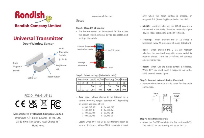
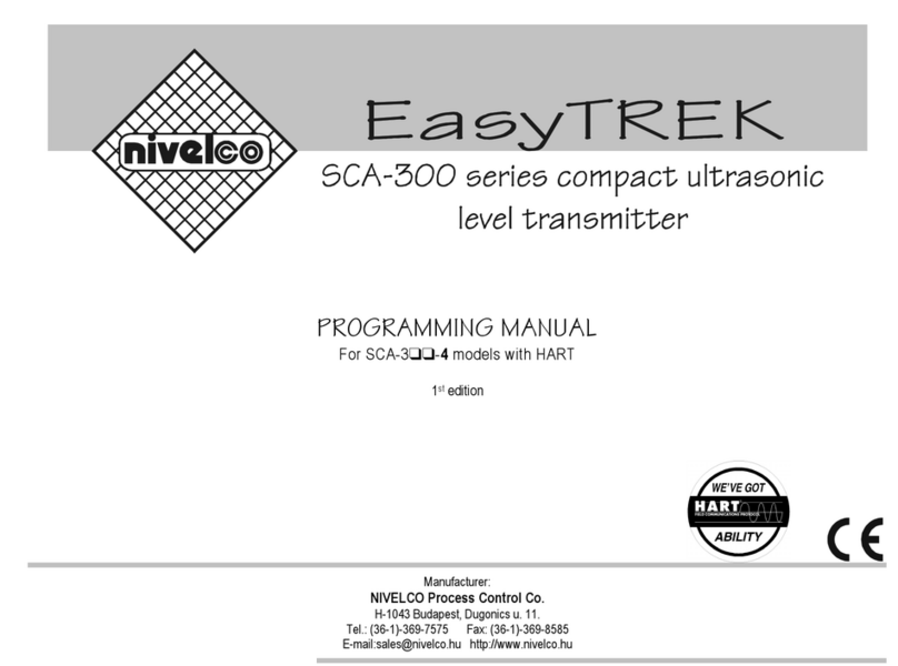
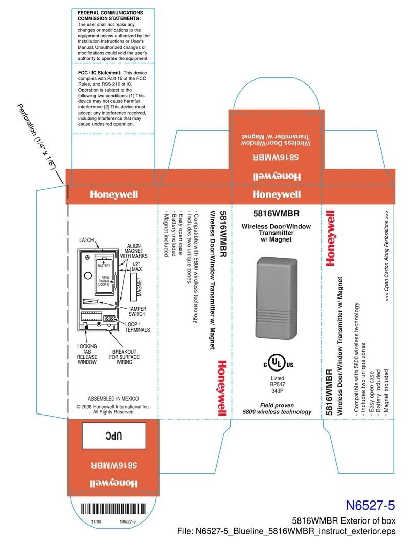
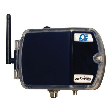
Sharp GP1A173LCS3F User manual

GP1A173LCS3F
1
Sheet No.: OP14021EN
GP1A173LCS3F is a standard, low voltage operation,
OPIC output, trans issive photointerrupter with
opposing e itter and detector in a case, providing
non-contact sensing.
For this fa ily of devices, the e itter and detector are
inserted in a case, and a 3-pin connector is included to
allow re ote- ount or off-board designs.
1. Trans issive with OPIC output
2. Highlights :
Special position hooks co patible with 3 different
Plate thicknesses (1.0, 1.2, 1.6 )
Snap insertion
3. Key Para eters :
Low operating voltage : 2.7 to 5.5V
Gap Width : 5
Slit Width (detector side) : 0.5
Package : 17 × 12.8 × 8 (without connector
and hooks)
Connector : Tyco Electronics JAPAN G.K.
(173977-3 and 179228-3)
4. RoHS directive co pliant
1. Co pliant with RoHS directive (2002/95/EC)
1. General purpose detection of object presence or
otion.
Exa ple : PPC, FAX, Printer
Description
Feature
s
Agency approvals/Compliance
Applications
Gap : 5.0mm, Slit : 0.5mm,
Low voltage operation,
*OPIC Output, Snap-in type
Compa t Transmissive
Photointerrupter
with onne tor
GP1A173LCS3F
*”OPIC”(Optical IC) is a trade ark of the SHARP Corporation. An OPIC consists of a light-detecting ele ent and
a signal-processing

GP1A173LCS3F
2
Sheet No.: OP14021
EN
Internal Connection Diagram
Outline
Drawing No. CY15164i02 Unit : 1/1
Note) 1. Unspecified tolerance shall be followed the list below.
2. Di ensions in parenthesis are shown for reference.
3. Coupling and contact : CT receptacle connector
(173977-3 and 179228-3) by Tyco Electronics Japan G.K.
4. Date code
Y : Year (2013 : 3) Last digit of prod. Year
M : Month (1 9, X, Y, Z)
D : Date (1 9, Please refer to a right list other than it.)
Di ension Tolerance
less than 5.0 ±0.15
5.0 or ore, less than 15.0 ±0.2
15.0 or ore ±0.3
Date
10 11 12 13 14
Code
A B C D E
Date
15 16 17 18 19
Code
F G H J K
Date
20 21 22 23 24
Code
M N O P R
Date
25 26 27 28 29
Code
S T U W X
Date
30 31
Code
Y Z
Vout
GND
Vcc

GP1A173LCS3F
3
Sheet No.: OP14021
EN
+0.3
-1.8
Absolute maximum ratings
Ta=25°C
Para eter Sy bol
Rating Unit
Re ark
Supply voltage Vcc -0.5 to +6 V
Output voltage Vout -0.5 to +6 V Output transistor between collector and e itter
Output current I
OL
8 A Output transistor collector current *1
Operating te perature Topr -30 to +95 °C The connector should be plugged in/out
at nor al te perature.
Storage te perature Tstg -40 to +100 °C
*1 Fig.1 shows output current vs. a bient te perature.
Electro-optical Characteristics
Vcc=3.3V, Ta=25°C
Para eter Sy bol
Rating Unit
Conditions
Current consu ption I
CCL
20 MAX. A Light bea uninterrupted
Low level output voltage V
OL
0.35 MAX V Light bea uninterrupted
I
OL
=4 A
Current consu ption I
CCH
20 MAX A Light bea interrupted
High level output voltage V
OH
Vcc×0.9 MIN
V Light bea interrupted
R
L
=10k
Operating voltage Vcc 2.7 to 5.5 V
Response
characteristics
Min. interrupted
ti e t
H
166 MIN s
R
L
=4.7k
Min. uninterrupted
ti e t
L
166 MIN s
Detection position characteristics
Ta=25°C, Vcc=3.3V, R
L
=10k
Horizontal detecting position characteristics Vertical detecting position characteristics
(d = 3.2±0.3 ) (d = 3.0 )
Output”High”
0 1 2 3 4 5 6 7
Distance d ( )
Output”Low”
Shield d
0
1
0
2
3
4
5
6
Distance d ( )
Output”High”
Output”Low”
d
0
Shield

GP1A173LCS3F
4
Sheet No.: OP14021
EN
Fig.1 Output current vs. a bient te perature

GP1A173LCS3F
5
Sheet No.: OP14021
EN
Supplements
ODS aterials
This product shall not contain the following aterials.
Also, the following aterials shall not be used in the production process for this product.
Materials for ODS : CFC
S
, Halon, Carbon tetrachloride 1.1.1-Trichloroethane (Methyl chlorofor )
Specified bro inated fla e retardants
Specified bro inated fla e retardants (PBB and PBDE) are not used in this device at all.
Co pliance with each regulation
1) The RoHS directive(2002/95/EC)
This product co plies with the RoHS directive(2002/95/EC).
Object substances: ercury, lead, cad iu , hexavalent chro iu , polybro inated biphenyls (PBB)
and polybro inated diphenyl ethers (PBDE)
2) Content of six substances specified in Manage ent Methods for Control of Pollution Caused by Electronic
Infor ation Products Regulation (Chinese : ).
Category
Toxic and hazardous substances
Lead
(Pb)
Mercury
(Hg)
Cad iu
(Cd)
Hexavalent
chro iu
(Cr
6+
)
Polybro inated
biphenyls
(PBB)
Polybro inated
diphenyl ethers
(PBDE)
Photointerrupter
: indicates that the content of the toxic and hazardous substance in all the ho ogeneous aterials of the part is
below the concentration li it require ent as described in SJ/T 11363-2006 standard.
Product ass : Approx. 1.0g
Country of origin : Philippine or China

GP1A173LCS3F
6
Sheet No.: OP14021
EN
4 or ore
Notes
Truth Table (In case of external addition pull-up resistance to Vout ter inal)
Light bea Output
Interrupted High
Uninterrupted Low
Power supply line
In order to stabilize power supply line, connect a by-pass capacitor of
ore than 0.01 F between Vcc and GND near the device.
Opaque board
Opaque board shall be installed at place 4 or ore fro the top of ele ents.
(Exa ple)
In case opaque board is the aterial with an low light blocking effect, There is a possibility of alfunctioning
because the light of LED trans its the opaque board. When you design the opaque board, please note trans ittance
of infrared rays wave length (950n ) and the thickness of the opaque board.
And, please adjust the a ount of trans itted light to 0.1% or less.
Cleaning
Please don't carry out i ersion cleaning or ultrasonic cleaning to avoid keeping solvent inside case of this device.
Washing aterial
Dust and stain shall clean by air blow, or shall clean by soft cloth soaked in washing aterials.
And washing aterial to clean shall be used the below aterials only.
Ethyl alcohol, Methyl alcohol, Isopropyl alcohol
Connector connection
For the electrical connection to the connector ter inal, please certainly use the connector specified
in this specifications.
Please avoid the connection by the soldering or welding which ay da age the ain body of the device,
and also avoid the contact by the clip and so on which ay cause the alfunction by the contact failure.
Please avoid the use condition that t it always occurs he vibration
in the spot where the connector fits in by the resonance of the sensor and the harness.
It ay cause the alfunction of the contact failure.
Put-in and pull-out of connector
The connection other than to the correct connection direction, forcing-into, and the pulling-out diagonally
(if being not put-in and pulled-out straight) ay defor or break the connector ter inal and/or housing,
which ay cause the unusable state of the device.
Interference light
Because the upper, botto and “Date Code” side are not covered by outer case,
please do not use this device under a bient light circu stances including infrared co ponent.

GP1A173LCS3F
7
Sheet No.: OP14021
EN
Recommended Installation Hole drawing
Unit : 1/1
(Drawing No. CY15165i06)
*1 We reco end to fix GP1A173LCS3F at punching side on the fixing plate ( etal plate).
*2 Please decide the final di ensions at your side after confir ation by the actual
applications, Because ounting efficiency and ounted stabilization are dependent
on ounting plate corner-R and punched state.
*3 Tolerance shall be ±0.1
*4 Please don’t hold connector area but sensor area when fitting in or putting out on the etal plate.
Nor al ounting type
Thickness of plate for 1.6 Thickness of plate for 1.2 Thickness of plate for 1.0
Irregular ounting protection type
Thickness of plate for 1.6 Thickness of plate for 1.2 Thickness of plate for 1.0

GP1A173LCS3F
8
Sheet No.: OP14021
EN
Parts
This product uses the below parts.
Light detector (Quantity : 1)
(Using a silicon photodiode as light detecting portion, and a bipolar IC as signal processing circuit.)
Type Maxi u sensitivity
wavelength (n )
Sensitivity
wavelength (n )
Response ti e
( s)
Photodiode 900 400 to 1200 10
Light e itter (Quantity : 1)
Type Material
Maxi u light e itting
wavelength (n )
I/O Frequency
(MHz)
Infrared light
e itting diode
(non-coherent)
GaAs 950 0.3
Material
Case Lead fla e
Black polycarbonate resin
(UL 94V-0)
Copper Alloy
(With plating)
Others
This product shall not be radiation flux proof.
The laser oscillator is not equipped on this product.
The ter inals are covered with Tin Plating ( ore than 99.99%).

GP1A173LCS3F
9
Sheet No.: OP14021
EN
Packing specification
Package
No.
Na e Material Quantity
1 Packing case Corrugated cardboard 1/1000
2 Pad Corrugated cardboard 6/1000
3 Tray Polystyrene 1/200
4 Kraft tape - -
Packing ethod
1) 5 products are put in 1 pocket.
The longer direction of the product is arranged in the arbitrary direction.
200 products are put in the tray. <Fig.1>
2) The pads are attached at the top and the botto of the trays
and also inserted between the trays. <Fig.2>
3) Seal packing case with Kraft tape. <Fig.3>
4) Indication ite s
The contents of the carton indication confor s to EIAJ C-3 and the following ite s are indicated.
Model No., Internal production control na e, Quantity, Packing date, Corporate na e,
Country of origin <Fig.3>
(1000pcs. / packing case)
(Approxi ately 2.26kg / packing ass)

GP1A173LCS3F
10
Sheet No.: OP14021
EN
Important Notices
· The circuit application exa ples in this publication are
provided to explain representative applications of SHARP
devices and are not intended to guarantee any circuit design or
license any intellectual property rights. SHARP takes no
responsibility for any proble s related to any intellectual
property right of a third party resulting fro the use of SHARP's
devices.
· Contact SHARP in order to obtain the latest device specification
sheets before using any SHARP device. SHARP reserves the
right to ake changes in the specifications, characteristics, data,
aterials, structure, and other contents described herein at any
ti e without notice in order to i prove design or reliability.
Manufacturing locations are also subject to change without
notice.
· Observe the following points when using any devices in this
publication. SHARP takes no responsibility for da age caused
by i proper use of the devices which does not eet the
conditions and absolute axi u ratings to be used specified in
the relevant specification sheet nor eet the following
conditions:
(i) The devices in this publication are designed for use in general
electronic equip ent designs such as:
--- Personal co puters
--- Office auto ation equip ent
--- Teleco unication equip ent [ter inal]
--- Test and easure ent equip ent
--- Industrial control
--- Audio visual equip ent
--- Consu er electronics
(ii) Measures such as fail-safe function and redundant design
should be taken to ensure reliability and safety when SHARP
devices are used for or in connection
with equip ent that requires higher reliability such as:
--- Transportation control and safety equip ent (i.e.,
aircraft, trains, auto obiles, etc.)
--- Traffic signals
--- Gas leakage sensor breakers
--- Alar equip ent
--- Various safety devices, etc.
(iii) SHARP devices shall not be used for or in connection with
equip ent that requires an extre ely high level of reliability and
safety such as:
--- Space applications
--- Teleco unication equip ent [trunk lines]
--- Nuclear power control equip ent
--- Medical and other life support equip ent (e.g.,
scuba).
· If the SHARP devices listed in this publication fall within the
scope of strategic products described in the Foreign Exchange
and Foreign Trade Law of Japan, it is necessary to obtain
approval to export such SHARP devices.
· This publication is the proprietary product of SHARP and is
copyrighted, with all rights reserved. Under the copyright laws,
no part of this publication ay be reproduced or trans itted in
any for or by any eans, electronic or echanical, for any
purpose, in whole or in part, without the express written
per ission of SHARP. Express written per ission is also
required before any use of this publication ay be ade by a
third party.
· Contact and consult with a SHARP representative if there are
any questions about the contents of this publication.
Table of contents