Shivaki FL32 Series User manual

SERVICE MANUAL
Model:
FL32xx(9E19 SOLUTION)
Safety Precaution
Technical Specifications
Block Diagram
Circuit Diagram
Main IC Specifications
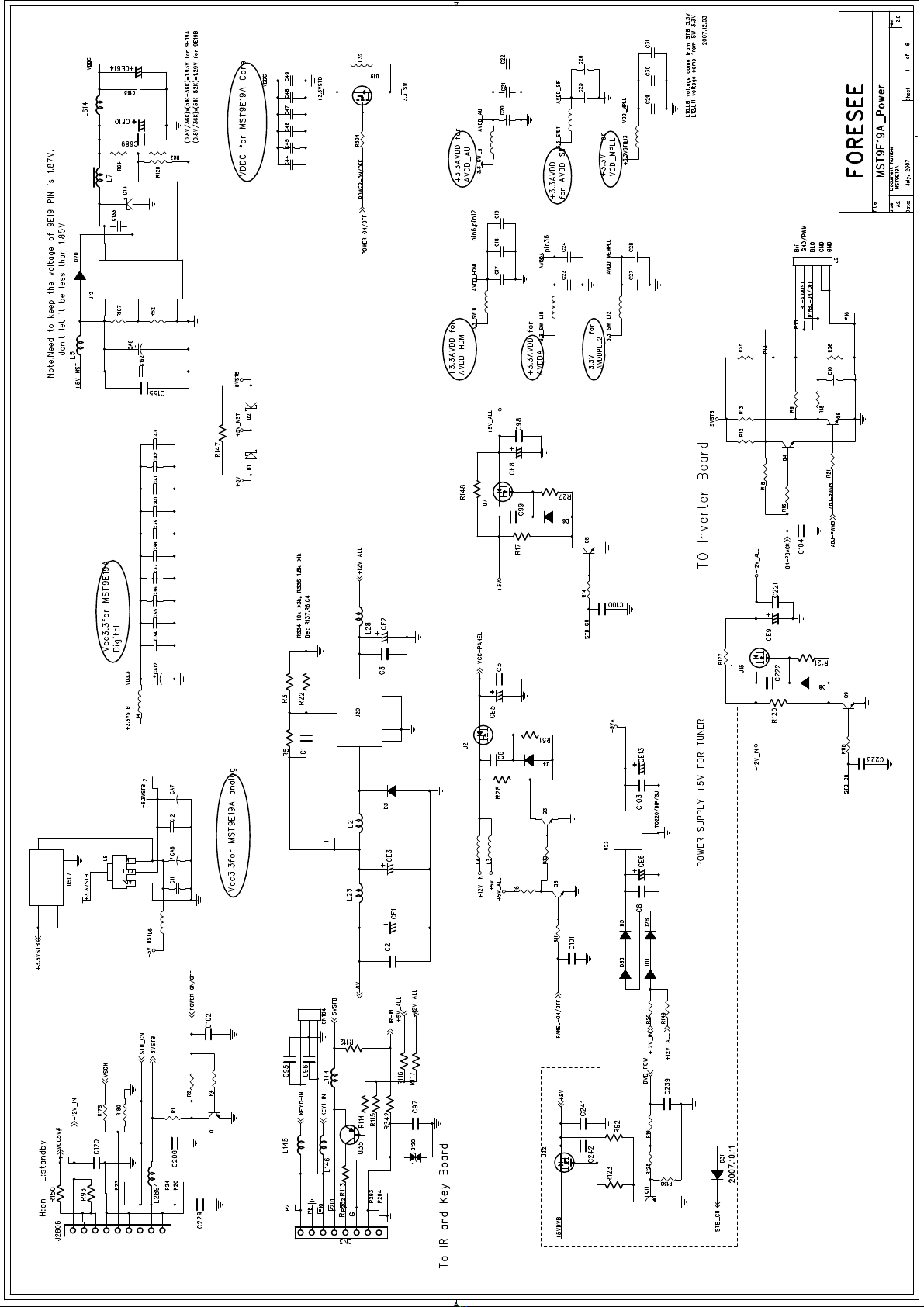
Power Supply Specification
Trouble Shooting
Software Upgrade
Enter Factory Menu
This manual is the latest at the time of printing, and does not
include the modification which may be made after the printing,
by the constant improvement of product.

IMPORTANT SAFETY INSTRUCTIONS
This symbol indicates dangerous voltage inside
the product that presents a risk of electric shock
or personal injury.
This symbol indicates important instructions
accompanying the product.
Please read thismanual carefully beforeusing this product.
Before connecting theAC powercord to theDC adapter outlet ,make sure the
voltage designation ofthe LCD TV corresponds tothe local electricalsupply .
If you areunsure of your power supply ,ask your local power company .
Never insert anythingmetallic into the cabinet openings ofthe liquid crystal
display LCD TV/monitor;otherwise it maycreate the danger of electric shock.
Toavoid electric shock, Never touch theinside of the LCD TV/monitor and adapter.
Only a qualifiedtechnician should open the case ofthe LCD TV/monitor/adapter.
Never use yourLCD TV/monitor/adapter if the powercord has beendamaged .
Do not allowanything to rest on the powercord, and keep the cord awayfrom
place where peoplecan trip over it .
Be sure tohold the plug, not the cord,when disconnecting the adapter from an
electric socket.
Openings in theLCD TV/monitor/adapter cabinet are providedfor ventilation.
Toprevent overheating, these openings should notbe blocked or covered. Also,
avoid using theLCD TV/monitor on a bed,sofa ,rug, orother soft surface.Doing
so may blockthe ventilation openings in the bottomof the cabinet. If you putthe
LCD TV/monitor in a bookcase or some other enclosed space, besure to provide
adequate ventilation.
Do not exposethe LCD TV/monitor to extremetemperature conditions or to
extreme humidity conditions.
The apparatus shallnot be exposed to dripping orsplashing and that no objects
filled with liquids,such as vases, shall be placedon the apparatus.

IMPORTANT SAFETY INSTRUCTIONS
Do not placethe LCD TV/monitor on an unstable cart, stand,tripod, bracket, table,or
floor where itcan fall. Itis damaged if dropped, hit orscratched. Do notclean the front
with keton-type materials(e.g.Acetone ),ethyl alcohol,toluene, ethy lacid, methyl, or
chloride-these may damage the panel.
Locate your DCadapter near aneasily accessible AC outlet.
If your LCDTV/monitor does not operate normally in particular,if there are any
unusual sounds orsmells coming fromit unplug it immediatelyand contact an
authorized dealer orservice enter.
High temperature cancause problems. Don`tuse your LCD TV/monitor in direct
sunlight, and keepit away fromheaters, stoves, fireplaces, and other sourcesof heat.
Unplug the DCadapter when itis going to be left unusedfor an extendedperiod of
time .
Toreduce the riskof fire or electric shock, andannoying interference, usethe
recommended accessories only.
If the LCDTV/monitor is broken, do not try to repairit yourself. Contactqualified
service personnel.
Unplug your DCadapter from theAC outlet before any service.
Be sure theservice technician usesauthorized replacement parts or their equivalents.
Unauthorized parts maycause fire, electricalshook, or other hazards.
Following any serviceor repair,be sure the service technician performssafety checks
to certify thatyour TFT-LCD TV/monitor is in safeoperating order.
The apparatus withCLASS I constructionshall be connected to a MAINSsocket outlet
with a protectiveearthing connection.
PRODUCT DESCRPTION OF 32" LCD TV
Model No. 32" LCD TV (MST9E19B Solution)
Panel LGLCDLC320WX1-SLA1 / CMO V320B1 - L06
Face color White/Dark blue
Screen size 32"
Resolution 1366(H) x 7680(V) pixels
Aspect ratio 16:9
Contrast Ratio 1000:1
Response Time(grey to grey) 10ms
Center Luminance of White 500cd/m2
Viewing Angle( L/R/U/D ) 88/88/88/88(CR≥20)
Power supply AC:(100-250)V 50/60Hz
Power Consumption ≤150W
Standy Power Consumption ≤1W
Broadcast PAL/SECAM BG/DK/I SECAM L/L'
Canal Plus Optional
Tuning system FST
Antenna impedance VHF/CATV/UHF 75Ωunbalanced
Teletext 200 pages
Number of channel 100
Sound
Nicam/A2 YES
Bass YES
Treble YES
Balance YES
Speakers 2
Audio power ≥2×5W
Connection jack
PC In (VGA) D-sub 15Pin × 1
Y/Pb/Pr Input RCA×3
Video Input ×1
S-video Input ×1
Audio In(For Y/Pb/Pr and Video) RCA×2
Audio In(For VGA and S-video) Φ3.5×1
Full Scart ×1
Half Scart ×1
RF ×1
HDMI Input x2
DVB-T Section (Optional)
DVB-T Channel Coverage 47MHz---862MHz
Constellation QPSK,16QAM,64QAM
Transmission Mode 2K,8K
Transport stream MPEG-2 ISO/IEC 13818
RF Bandwidth 7MHz or 8MHz
Input Rate Max. 15M/bits
Common interface Optional
Others
Last Channel recall YES
Automatic tuning YES
Sleep timer YES
OSD Menu Multi-language
Comb filter 2D
Mounting interface Vesa Standard
Standard Accessories
User Manual 1
Remote control 1
Optional Accessories
Wall mounting holder 1

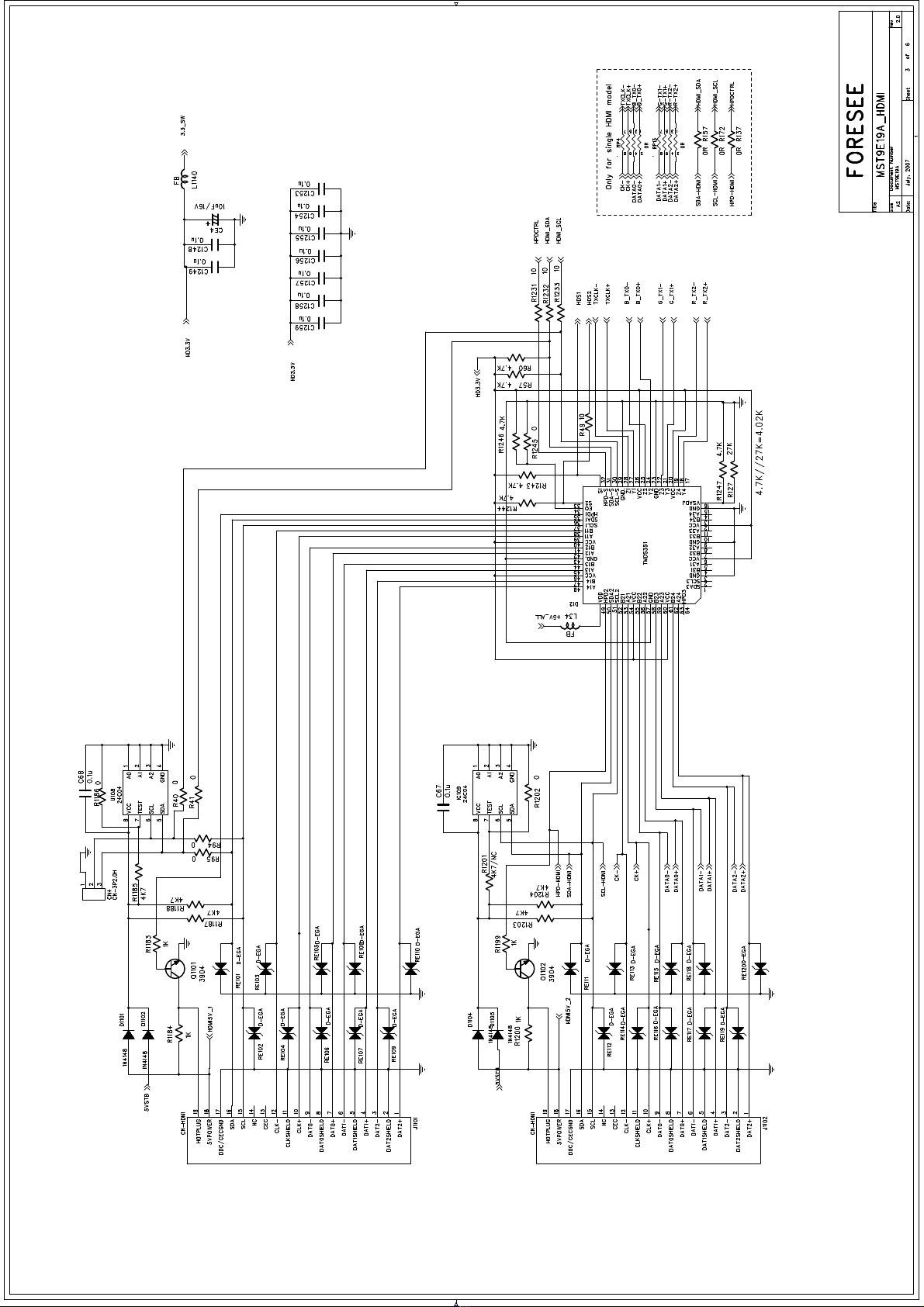


MST9E19A
SXGA/WXGA+ LCD TV Controller with Video Decoder & 10-bit Dual LVDS Transmitter
PIN DESCRIPTION
MCU Interface
Pin Name Pin Type Function Pin
HWRESET Schmitt Trigger Input
w/ 5V-tolerant
Hardware Reset, active high 205
ALE I/O w/ 5V-tolerant MCU Bus ALE, active high /
General Purpose Input/Output (GPIOC[10])
118
RDZ I/O w/ 5V-tolerant MCU Bus RDZ, active low /
General Purpose Input/Output (GPIOC[9])
117
WRZ I/O w/ 5V-tolerant MCU Bus WDZ, active low /
General Purpose Input/Output (GPIOC[8])
116
INT I/O w/ 5V-tolerant MCU Bus Interrupt; 4mA driving strength /
General Purpose Output (GPIOD[12])
135
AD[7:0] I/O w/ 5V-tolerant 8051 bus AD[7:0]; 4mA driving strength /
External Flash/RAM Data Bus (FLSHD[7:0]) /
General Purpose Input/Output (GPIOC[7:0])
115-108
Analog Interface
Pin Name Pin Type Function Pin
RMID Mid-Scale Voltage Bypass 18
VCLAMP CVBS/YC Mode Clamp Voltage Bypass 19
REFP Internal ADC Top De-coupling Pin 20
REFM Internal ADC Bottom De-coupling Pin 21
REXT Analog Input External Resister 390 ohm to AVDD_DVI 13
HSYNC0 Schmitt Trigger Input
w/ 5V-tolerant
Analog HSYNC Input from Channel 0 /
Function Select Switch Input from Channel 0 (FSSW0)
38
VSYNC0 Schmitt Trigger Input
w/ 5V-tolerant
Analog VSYNC Input from Channel 0 /
Fast Blanking Input from Channel 0 (FBLK0)
39
BIN0M Analog Input Reference Ground for Analog Blue Input from Channel 0 29
BIN0P Analog Input Analog Blue Input from Channel 0 30
GIN0M Analog Input Reference Ground for Analog Green Input from Channel
0
31
GIN0P Analog Input Analog Green Input from Channel 0 32
SOGIN0 Analog Input Sync On Green Input from Channel 0 33
RIN0M Analog Input Reference Ground for Analog Red Input from Channel 0 34
RIN0P Analog Input Analog Red Input from Channel 0 35
HSYNC1 Schmitt Trigger Input Analog HSYNC Input from Channel 1 / 16

MST9E19A
SXGA/WXGA+ LCD TV Controller with Video Decoder & 10-bit Dual LVDS Transmitter
Pin Name Pin Type Function Pin
w/ 5V-tolerant Function Select Switch Input from Channel 1 (FSSW1)
/VSYNC1 Schmitt Trigger Input
w/ 5V-tolerant
Analog VSYNC Input from Channel 1 /
Fast Blanking Input from Channel 1 (FBLK1)
17
BIN1M Analog Input Reference Ground for Analog Blue Input from Channel 1 23
BIN1P Analog Input Analog Blue Input from Channel 1 22
SOGIN1 Analog Input Sync On Green Input from Channel 1 24
GIN1M Analog Input Reference Ground for Analog Green Input from Channel
1
26
GIN1P Analog Input Analog Green Input from Channel 1 25
RIN1M Analog Input Reference Ground for Analog Red Input from Channel 1 28
RIN1P Analog Input Analog Red Input from Channel 1 27
Analog Video Input/Output Interface
Pin Name Pin Type Function Pin
C1 Analog Input Chroma Video Input 1 /
CVBS Input Channel 7 (CVBS7)
40
Y1 Analog Input Luma Video Input 1 /
CVBS Input Channel 5 (CVBS5)
41
C0 Analog Input Chroma Video Input 0 /
CVBS Input Channel 6 (CVBS6)
42
Y0 Analog Input Luma Video Input 0 /
CVBS Input Channel 4 (CVBS4)
43
VCOM2 Analog Input YC Video Input Reference Ground 44
VCOM1 Analog Input CVBS1, CVBS2, CVBS3 Video Input Reference Ground 48
VCOM0 Analog Input CVBS0 Video Input Reference Ground 50
CVBS3 Analog Input CVBS (Composite) Video Input Channel 3 45
CVBS2 Analog Input CVBS (Composite) Video Input Channel 2 46
CVBS1 Analog Input CVBS (Composite) Video Input Channel 1 47
CVBS0 Analog Input CVBS (Composite) Video Input Channel 0 49
CVBSOUT Analog Output CVBS (Composite) Video Output 51
Analog Audio Input/Output Interface
Pin Name Pin Type Function Pin
SIF1M Analog Input Reference Ground for SIF Audio Input 55
SIF1P Analog Input SIF Audio Input 54
AUVRADN Negative Reference Ground for Audio ADC 57

MST9E19A
SXGA/WXGA+ LCD TV Controller with Video Decoder & 10-bit Dual LVDS Transmitter
Pin Name Pin Type Function Pin
AUVRADP Positive Reference Voltage for Audio ADC 58
AUVREF Reference Voltage for Audio Common Mode 59
AUL0 Analog Input Audio Line Input Left Channel 0 61
AUR0 Analog Input Audio Line Input Right Channel 0 62
AUL1 Analog Input Audio Line Input Left Channel 1 63
AUR1 Analog Input Audio Line Input Right Channel 1 64
AUCOM Analog Input Reference Ground for Audio Line Input 65
AUL2 Analog Input Audio Line Input Left Channel 2 66
AUR2 Analog Input Audio Line Input Right Channel 2 67
AUL3 Analog Input Audio Line Input Left Channel 3 68
AUR3 Analog Input Audio Line Input Right Channel 3 69
AUOUTL3 Analog Output Main Audio Output Left Channel 3 70
AUOUTR3 Analog Output Main Audio Output Right Channel 3 71
AUOUTL2 Analog Output Main Audio Output Left Channel 2 72
AUOUTR2 Analog Output Main Audio Output Right Channel 2 73
AUOUTL Analog Output Main Audio Output Left Channel 74
AUOUTR Analog Output Main Audio Output Right Channel 75
AUOUTS Analog Output Main Audio Sub-Woofer Channel 76
DVI/HDMI Interface
Pin Name Pin Type Function Pin
RX0N Analog Input DVI/HDMI Channel 0 Negative Data Input 4
RX0P Analog Input DVI/HDMI Channel 0 Positive Data Input 5
RX1N Analog Input DVI/HDMI Channel 1 Negative Data Input 7
RX1P Analog Input DVI/HDMI Channel 1 Positive Data Input 8
RX2N Analog Input DVI/HDMI Channel 2 Negative Data Input 10
RX2P Analog Input DVI/HDMI Channel 2 Positive Data Input 11
RXCKN Analog Input DVI/HDMI Negative Clock Input 1
RXCKP Analog Input DVI/HDMI Positive Clock Input 2
LVDS Interface Note 1
Pin Name Pin Type Function Pin
LVA0M Output LVDS A-Link Channel 0 Negative Data Output 171
LVA0P Output LVDS A-Link Channel 0 Positive Data Output 170
LVA1M Output LVDS A-Link Channel 1 Negative Data Output 169

MST9E19A
SXGA/WXGA+ LCD TV Controller with Video Decoder & 10-bit Dual LVDS Transmitter
.
Pin Name Pin Type Function Pin
LVA1P Output LVDS A-Link Channel 1 Positive Data Output 168
LVA2M Output LVDS A-Link Channel 2 Negative Data Output 167
LVA2P Output LVDS A-Link Channel 2 Positive Data Output 166
LVA3M Output LVDS A-Link Channel 3 Negative Data Output 163
LVA3P Output LVDS A-Link Channel 3 Positive Data Output 162
LVA4M Output LVDS A-Link Channel 3 Negative Data Output 161
LVA4P Output LVDS A-Link Channel 3 Positive Data Output 160
LVACKM Output LVDS A-Link Negative Clock Output 165
LVACKP Output LVDS A-Link Positive Clock Output 164
LVB0M Output LVDS B-Link Channel 0 Negative Data Output 185
LVB0P Output LVDS B-Link Channel 0 Positive Data Output 184
LVB1M Output LVDS B-Link Channel 1 Negative Data Output 183
LVB1P Output LVDS B-Link Channel 1 Positive Data Output 182
LVB2M Output LVDS B-Link Channel 2 Negative Data Output 181
LVB2P Output LVDS B-Link Channel 2 Positive Data Output 180
LVB3M Output LVDS B-Link Channel 3 Negative Data Output 177
LVB3P Output LVDS B-Link Channel 3 Positive Data Output 176
LVB4M Output LVDS B-Link Channel 3 Negative Data Output 175
LVB4P Output LVDS B-Link Channel 3 Positive Data Output 174
LVBCKM Output LVDS B-Link Negative Clock Output 179
LVBCKP Output LVDS B-Link Positive Clock Output 178
Note 1: Please see the Output Type vs. Pin Configuration at the end of Pin Description section.
TTL Interface Note 1
Pin Name Pin Type Function Pin
LCK Output w/ Pull-down
Resistor
LCD Output Clock; 6mA driving strength 188
LDE Output w/ Pull-down
Resistor
LCD Output Data Enable; 6mA driving strength 189
LHSYNC Output w/ Pull-down
Resistor
LCD HSYNC; 6mA driving strength 190
LVSYNC Output w/ Pull-down
Resistor
LCD VSYNC; 6mA driving strength 191
RA[7:0] Output w/ Pull-down
Resistor
Port A Red Channel Bit[7:0]; 6mA driving strength 185-178
GA[7:0] Output w/ Pull-down Port A Green Channel Bit[7:0]; 6mA driving 177-174,
MST9E19A
SXGA/WXGA+ LCD TV Controller with Video Decoder & 10-bit Dual LVDS Transmitter
.
Pin Name Pin Type Function Pin
Resistor strength 171-168
BA[7:0] Output w/ Pull-down
Resistor
Port A Blue Channel Bit[7:0]; 6mA driving strength 167-160
Note 1: Please see the Output Type vs. Pin Configuration at the end of Pin Description section.
Serial Flash Interface
Pin Name Pin Type Function Pin
SCK I/O w/ 5V-tolerant SPI Flash Serial Clock /
General Purpose Input/Output (GPIOD[14])
121
SDI I/O w/ 5V-tolerant SPI Flash Serial Data Input (Output Pin) /
General Purpose Input/Output (GPIOD[15])
122
CSZ I/O w/ 5V-tolerant SPI Flash Chip select /
General Purpose Input/Output (GPIOD[16])
123
SDO I/O w/ 5V-tolerant SPI Flash Serial Data Output (Input Pin) /
General Purpose Input/Output (GPIOD[17])
124
GPIO Interface Note 2
Pin Name Pin Type Function Pin
SAR3 I/O (not 5V-tolerant) SAR Low Speed ADC Input 3 /
General Purpose Input/Output (GPIOD[3])
128
SAR2 I/O (not 5V-tolerant) SAR Low Speed ADC Input 2 /
General Purpose Input/Output (GPIOD[2])
127
SAR1 I/O (not 5V-tolerant) SAR Low Speed ADC Input 1 /
General Purpose Input/Output (GPIOD[1])
126
SAR0 I/O (not 5V-tolerant) SAR Low Speed ADC Input 0 /
General Purpose Input/Output (GPIOD[0])
125
PWM3 I/O w/ 5V-Tolerant Pulse Width Modulation Output 3; 4mA driving
strength /
General Purpose Output (GPIOD[7])
156
PWM2 I/O w/ 5V-Tolerant Pulse Width Modulation Output 2; 4mA driving
strength /
General Purpose Output (GPIOD[6])
155
PWM1 I/O w/ 5V-Tolerant Pulse Width Modulation Output 1; 4mA driving
strength /
General Purpose Output (GPIOD[5])
130
PWM0 I/O w/ 5V-Tolerant Pulse Width Modulation Output 0; 4mA driving
strength /
General Purpose Output (GPIOD[4])
129

MST9E19A
SXGA/WXGA+ LCD TV Controller with Video Decoder & 10-bit Dual LVDS Transmitter
Pin Name Pin Type Function Pin
IRIN I/O w/ 5V-tolerant IR Receiver Input /
General Purpose Output (GPIOD[13])
136
DIGO[9:6] I/O w/ 5V-tolerant General Purpose Input/Output (GPIOB[9:6]) 154, 153,
150, 149
DIGO[5] I/O w/ 5V-tolerant General Purpose Input/Output (GPIOB[5]) /
Universal Asynchronous Transmitter 1 (UART1_TX)
148
DIGO[4] I/O w/ 5V-tolerant General Purpose Input/Output (GPIOB[4]) /
Universal Asynchronous Receiver 1 (UART1_RX)
147
DIGO[3] I/O w/ 5V-tolerant General Purpose Input/Output (GPIOB[3]) /
Programmable as Audio Serial Data Output 0
(AU2SD0)
146
DIGO[2] I/O w/ 5V-tolerant General Purpose Input/Output (GPIOB[2]) /
Programmable as Audio Serial Clock Output (AU2SCK)
145
DIGO[1] I/O w/ 5V-tolerant General Purpose Input/Output (GPIOB[1]) /
Programmable as Word Select Output (AU2WS)
144
DIGO[0] I/O w/ 5V-tolerant General Purpose Input/Output (GPIOB[0]) /
Programmable as Audio Master Clock Output
(AU2MCKO)
143
ICLK I/O w/ 5V-tolerant Digital Input Clock /
Universal Asynchronous Receiver 0 (UART0_RX) /
General Purpose Input/Output (GPIOA[24])
192
IHSYNC I/O w/ 5V-tolerant Digital Input HSYNC /
Universal Asynchronous Receiver 1 (UART1_RX) /
General Purpose Input/Output (GPIOA[26])
193
IVSYNC I/O w/ 5V-tolerant Digital Input VSYNC /
Universal Asynchronous Transmitter 1 (UART1_TX) /
General Purpose Input/Output (GPIOA[27])
194
DI[7:0] I/O w/ 5V-tolerant Video Digital Input Port /
Digital Audio Port /
General Purpose Input/Output (GPIOA[15:0])
202-195
GPIOE[3:0] I/O w/ 5V-tolerant General Purpose Input/Output (GPIOE[3:0]) 188-191
GPIOF[19:2] I/O w/ 5V-tolerant General Purpose Input/Output (GPIOF[2:19]) 97-90,
87-78
Note 2: Please see Pin Configuration vs. Function at the end of Pin Description section.
PWM Regulator Interface
Pin Name Pin Type Function Pin
PWM_FB Analog Input Step-down PWM Feedback 137
PWM_DRV I/O Step-down PWM Drive 138

MST9E19A
SXGA/WXGA+ LCD TV Controller with Video Decoder & 10-bit Dual LVDS Transmitter
Pin Name Pin Type Function Pin
PWM_SENSE Analog Input Step-down PWM Sense 139
Misc. Interface
Pin Name Pin Type Function Pin
DDCD_DA I/O w/ 5V-tolerant HDCP Serial Bus Data / DDC Data of DVI Port 14
DDCD_CK Input w/ 5V-tolerant HDCP Serial Bus Clock / DDC Clock of DVI Port 15
DDCA_CK I/O w/ 5V-tolerant DDC Clock for Analog port /
Universal Asynchronous Receiver 0 (UART0_RX)/
General Purpose Output (GPIOD[11])
134
DDCA_DA I/O w/ 5V-tolerant DDC Data for Analog port /
Universal Asynchronous Transmitter 0 (UART0_TX) /
General Purpose Output (GPIOD[10])
133
DDCR_CK I/O w/ 5V-tolerant DDC Clock for ROM /
General Purpose Output (GPIOD[9])
132
DDCR_DA I/O w/ 5V-tolerant DDC Data for ROM /
General Purpose Output (GPIOD[8])
131
XIN Crystal Oscillator Input Crystal Oscillator Input 207
XOUT Crystal Oscillator
Output
Crystal Oscillator Output 206
Power Pins
Pin Name Pin Type Function Pin
AVDD_DVI 3.3V Power DVI Power 6, 12
AVDD_ADC 3.3V Power ADC Power 36
AVDD_SIF 3.3V Power SIF Power 53
AVDD_AU 3.3V Power Audio Power 60
AVDD_MEMPLL 3.3V Power PLL Power 105
AVDD_MPLL 3.3V Power PLL Power 157, 208
VDDP 3.3V Power Digital Output Power 88, 100, 102, 103, 119,
140, 151, 159, 172,
186
VDDC 1.8V Power Digital Core Power 77, 98, 107, 142, 158,
203
GND Ground Ground 3, 9, 37, 52, 56, 89, 99,
101, 104, 106, 120,
141, 152, 173, 187, 204

Dimension Diagram
Terminals Name
Pin No Pin Name Description
1 NC -----
2 BT OPEN
3 VCC2 5.0V (MAX 150mA)
4 SCL -----
5 SDA -----
6 AS -----
7 AFC -----
8 NC -----
9 NC -----
10 NC -----
11 2nd SIF Output -----
12 Video Output -----
13 VCC3 5.0V(MAX 170mA)
14 Audio Output
TUNER DATASHEET

03&
7UXWK7DEOH
(1 ,1 216ZLWFK
6$6%6&6'
6$6%6&6'
; 'LVDEOHG
)HDWXUHV
+LJKSHUIRUPDQFHVROXWLRQWRVZLWFKEHWZHHQYLGHRVRXUFHV
:LGHEDQGZLGWK0+]
/RZ2Q5HVLVWDQFH
/RZFURVVWDONDW0+]±G%
8OWUDORZTXLHVFHQWSRZHU$W\SLFDO
6LQJOHVXSSO\RSHUDWLRQ9
)DVWVZLWFKLQJQV
+LJKFXUUHQWRXWSXWP$
3DFNDJLQJ3EIUHH*UHHQ$YDLODEOH
±SLQPLOZLGHSODVWLF62,&6
±SLQPLOZLGHSODVWLF62,&:
±SLQPLOZLGHSODVWLF46234
3,9
/RZ2Q5HVLVWDQFH:LGHEDQG9LGHR
4XDG&KDQQHO0X['H0X[
%ORFN'LDJUDP
'HVFULSWLRQ
3HULFRP6HPLFRQGXFWRU¶V 3,9LV DWUXH ELGLUHFWLRQDO4XDG
FKDQQHOPXOWLSOH[HUGHPXOWLSOH[HUUHFRPPHQGHGIRUERWK5*%
DQGFRPSRVLWHYLGHRVZLWFKLQJDSSOLFDWLRQV7KHYLGHRVZLWFKFDQ
EHGULYHQIURPDFXUUHQWRXWSXW5$0'$&RUYROWDJHRXWSXWFRP
SRVLWHYLGHRVRXUFH
/RZ2Q5HVLVWDQFHDQGZLGHEDQGZLGWKPDNHLWLGHDOIRUYLGHRDQG
RWKHUDSSOLFDWLRQV$OVRWKLVGHYLFHKDVH[FHSWLRQDOO\KLJKFXUUHQW
FDSDELOLW\ZKLFKLVIDUJUHDWHUWKDQPRVWDQDORJVZLWFKHVRIIHUHG
WRGD\$VLQJOH9VXSSO\LVDOOWKDWLVUHTXLUHGIRURSHUDWLRQ
7KH 3,9 RIIHUV D KLJKSHUIRUPDQFH ORZFRVW VROXWLRQ WR
VZLWFKEHWZHHQYLGHRVRXUFHV7KHDSSOLFDWLRQVHFWLRQGHVFULEHVWKH
3,9UHSODFLQJWKH+&PXOWLSOLHUDQGEXIIHUDPSOL¿HU
3LQ&RQ¿JXUDWLRQ
3LQ'HVFULSWLRQ
3LQ1DPH 'HVFULSWLRQ
6$6%6&6'
6$6%6&6'$QDORJ9LGHR,2
,1 6HOHFW,QSXW
(1 (QDEOH
'$'%
'&''$QDORJ9LGHR,2
*1' *URXQG
9&& 3RZHU
9&&
(1
6'
6'
''
6&
6&
'&
,1
6$
6$
'$
6%
6%
'%
*1'
'$
6$
6$
'%
6%
6%
'&
6&
6&
''
6'
6'
'(&2'(5'5,9(56
(1 ,1
This manual suits for next models
1
Table of contents
Other Shivaki LCD TV manuals


