Signal Recovery 7210 User manual

Model 7210
Multi-Channel
DSP Lock-in Amplifier
Instruction Manual
190480-A-MNL-F
Acknowledgement
This instrument was originally developed in conjunction with:
Dr E. Tokunaga
Masumoto Single Quantum Dot Project
Japan Science and Technology Corporation
Tsukuba Research Consortium
5-9-9 Tokodai
Tsukuba
Ibaraki 300-2635
Japan
Copyright © 2013 AMETEK ADVANCED MEASUREMENT TECHNOLOGY, INC

FCC Notice
This equipment generates, uses, and can radiate radio
used in accordance with this manual, may cause interference to radio communications. As
temporarily permitted by regulation, operation of this equipment in a residential area is likely to
cause interference, in which case the user at his own facility w
measures may be required to correct the interference.
Company Names
SIGNAL RECOVERY
is part of Advanced Measurement Technology, Inc, a division of AMETEK,
Inc. It includes the businesses formerly trading as EG&G Princeton
Instruments (Signal Recovery), EG&G Signal Recovery and PerkinElmer Instruments (Signal
Recovery)
Declaration of Conformity
This product conforms to EC Directives 89/336/EEC Electromagnetic Compatibility Directive,
amended by 92/31/
EEC and 93/68/EEC, and Low Voltage Directive 73/23/EEC amended by
93/68/EEC.
This product has been designed in conformance with the following IEC/EN standards:
EMC:
BS EN55011 (1991) Group 1, Class A (CSPIR 11:1990)
BS EN50082-
1 (1992):
IEC 801
IEC 801
IEC 801
Safety: BS EN61010-
1: 1993 (IEC 1010
Trademarks
AMETEK® and the and
logos are registered trademarks of
This equipment generates, uses, and can radiate radio
-
frequency energy and, if not installed
used in accordance with this manual, may cause interference to radio communications. As
temporarily permitted by regulation, operation of this equipment in a residential area is likely to
cause interference, in which case the user at his own facility w
ill be required to take whatever
measures may be required to correct the interference.
is part of Advanced Measurement Technology, Inc, a division of AMETEK,
Inc. It includes the businesses formerly trading as EG&G Princeton
Applied Research, EG&G
Instruments (Signal Recovery), EG&G Signal Recovery and PerkinElmer Instruments (Signal
This product conforms to EC Directives 89/336/EEC Electromagnetic Compatibility Directive,
EEC and 93/68/EEC, and Low Voltage Directive 73/23/EEC amended by
This product has been designed in conformance with the following IEC/EN standards:
BS EN55011 (1991) Group 1, Class A (CSPIR 11:1990)
1 (1992):
IEC 801
-2:1991
IEC 801
-3:1994
IEC 801
-4:1988
1: 1993 (IEC 1010
-1:1990+A1:1992)
logos are registered trademarks of
AMETEK, Inc.
frequency energy and, if not installed
and
used in accordance with this manual, may cause interference to radio communications. As
temporarily permitted by regulation, operation of this equipment in a residential area is likely to
ill be required to take whatever
is part of Advanced Measurement Technology, Inc, a division of AMETEK,
Applied Research, EG&G
Instruments (Signal Recovery), EG&G Signal Recovery and PerkinElmer Instruments (Signal
This product conforms to EC Directives 89/336/EEC Electromagnetic Compatibility Directive,
EEC and 93/68/EEC, and Low Voltage Directive 73/23/EEC amended by
This product has been designed in conformance with the following IEC/EN standards:

Table of Contents Table of Contents
i
Chapter One, Introduction
1.1 How to Use This Manual.................................................................................................................................. 1-1
1.2 What is a Lock-in Amplifier?........................................................................................................................... 1-2
1.3 Key Specifications and Benefits....................................................................................................................... 1-2
Chapter Two, Installation & Initial Checks
2.1 Installation........................................................................................................................................................ 2-1
2.1.01 Introduction ............................................................................................................................................. 2-1
2.1.02 Inspection ................................................................................................................................................ 2-1
2.1.03 Line Cord Plug......................................................................................................................................... 2-1
2.1.04 Line Voltage Selection and Line Fuses................................................................................................... 2-1
2.2 Initial Checks.................................................................................................................................................... 2-3
2.2.01 Introduction ............................................................................................................................................. 2-3
2.2.02 Procedure................................................................................................................................................. 2-3
Chapter Three, Technical Description
3.1 Introduction ...................................................................................................................................................... 3-1
3.2 Operating Modes .............................................................................................................................................. 3-1
3.2.01 Introduction ............................................................................................................................................. 3-1
3.2.02 Single Reference Mode ........................................................................................................................... 3-1
3.2.03 Tandem Reference Mode......................................................................................................................... 3-1
3.3 Principles of Operation..................................................................................................................................... 3-2
3.3.01 Block Diagram......................................................................................................................................... 3-2
3.3.02 Signal Channel Inputs.............................................................................................................................. 3-3
3.3.03 AC Gain and Dynamic Reserve............................................................................................................... 3-3
3.3.04 Anti-Aliasing Filter.................................................................................................................................. 3-4
3.3.05 Main Analog-to-Digital Converter.......................................................................................................... 3-5
3.3.06 Reference Channel................................................................................................................................... 3-6
3.3.07 Phase-Shifters.......................................................................................................................................... 3-6
3.3.08 Demodulator DSP.................................................................................................................................... 3-6
3.3.09 Main Microprocessor - General............................................................................................................... 3-7
3.3.10 Main Microprocessor - Auto Functions................................................................................................... 3-7
3.3.11 Main Microprocessor - Curve Buffer...................................................................................................... 3-9
3.4 General ............................................................................................................................................................. 3-9
3.4.01 Accuracy.................................................................................................................................................. 3-9
3.4.02 Power-up Defaults................................................................................................................................... 3-9
Chapter Four, Front and Rear Panels
4.1 Front Panel........................................................................................................................................................ 4-1
4.1.01 Signal Input Connectors.......................................................................................................................... 4-1
4.1.02 REF 1 IN Connector................................................................................................................................ 4-1
4.1.03 REF 2 OUT Connector............................................................................................................................ 4-1
4.1.04 TRIG 1 and TRIG 2 Connectors.............................................................................................................. 4-2

TABLE OF CONTENTS
ii
4.1.05 Indicators................................................................................................................................................. 4-2
4.2 Rear Panel......................................................................................................................................................... 4-3
4.2.01 Line Power Switch .................................................................................................................................. 4-3
4.2.02 Line Power Input Assembly.................................................................................................................... 4-3
4.2.03 RS232 Connector .................................................................................................................................... 4-3
4.2.04 GPIB Connector...................................................................................................................................... 4-3
4.2.05 DIGITAL I/O Connector......................................................................................................................... 4-3
4.2.06 PREAMP POWER Connector ................................................................................................................ 4-4
4.2.07 LINK 1 and LINK 2 connectors.............................................................................................................. 4-4
4.2.08 GPIB Address & Master/Slave Switch.................................................................................................... 4-4
Chapter Five, Computer Operation
5.1 Introduction...................................................................................................................................................... 5-1
5.2 RS232 and GPIB Operation............................................................................................................................. 5-1
5.2.01 Introduction............................................................................................................................................. 5-1
5.2.02 RS232 Interface - General Features ........................................................................................................ 5-1
5.2.03 Choice of Baud Rate................................................................................................................................ 5-2
5.2.04 Choice of Number of Data Bits............................................................................................................... 5-2
5.2.05 Choice of Parity Check Option................................................................................................................ 5-3
5.2.06 GPIB Interface - General Features.......................................................................................................... 5-3
5.2.07 Handshaking and Echoes......................................................................................................................... 5-3
5.2.08 Terminators ............................................................................................................................................. 5-5
5.2.09 Command Format.................................................................................................................................... 5-5
5.2.10 Delimiters................................................................................................................................................ 5-6
5.2.11 Compound Commands............................................................................................................................ 5-6
5.2.12 Status Byte, Prompts and Overload Byte................................................................................................ 5-6
5.2.13 Service Requests...................................................................................................................................... 5-8
5.3 Command Descriptions.................................................................................................................................... 5-8
5.3.01 Signal Channel ........................................................................................................................................ 5-9
5.3.02 Reference Channel ................................................................................................................................ 5-12
5.3.03 Signal Channel Output Filters............................................................................................................... 5-13
5.3.04 Instrument Outputs................................................................................................................................ 5-14
5.3.05 Auxiliary Output.................................................................................................................................... 5-15
5.3.06 Output Data Curve Buffer..................................................................................................................... 5-15
5.3.07 Computer Interfaces (RS232 and GPIB)............................................................................................... 5-23
5.3.08 Instrument Identification....................................................................................................................... 5-25
5.3.09 Auto Default.......................................................................................................................................... 5-25
5.4 Programming Examples ................................................................................................................................. 5-26
5.4.01 Introduction........................................................................................................................................... 5-26
5.4.02 Basic Signal Recovery - Single Reference Mode.................................................................................. 5-26
5.4.03 Basic Signal Recovery - Tandem Reference Mode............................................................................... 5-26
5.4.04 Tandem Reference Mode with Output Data Sampling Correlation ...................................................... 5-27
Appendix A, Specifications

TABLE OF CONTENTS
iii
Appendix B, Pinouts
B1 RS232 Connector Pinout ..................................................................................................................................B-1
B2 Digital Output Port Connector..........................................................................................................................B-1
B3 Preamplifier Power Connector Pinout..............................................................................................................B-1
Appendix C, Demonstration Programs
C1 Simple Terminal Emulator................................................................................................................................C-1
C2 RS232 Control Program with Handshakes .......................................................................................................C-1
C3 GPIB User Interface Program...........................................................................................................................C-3
Appendix D, Cable Diagrams
D1 RS232 Cable Diagrams......................................................................................................................................D1
Appendix E, Alphabetical Listing of Commands
Index
Warranty
...................................................................................................................................... End of Manual


Introduction Chapter
1
1-1
1.1 How to Use This Manual
This manual gives detailed instructions for setting up and operating the
SIGNAL RECOVERY Model 7210 Multi-Channel Digital Signal Processing (DSP)
dual phase lock-in amplifier. It is split into the following chapters:-
Chapter 1 - Introduction
Provides an introduction to the manual, briefly describes what a lock-in amplifier is
and the types of measurements it may be used for, and lists the major specifications
of the model 7210.
Chapter 2 - Installation and Initial Checks
Describes how to install the instrument and gives a simple test procedure which may
be used to check that the unit has arrived in full working order.
Chapter 3 - Technical Description
Provides an outline description of the design of the instrument and discusses the
effect of the various controls. A good understanding of the design will enable the user
to get the best possible performance from the unit.
Chapter 4 - Front and Rear Panels
Describes the connectors, controls and indicators which are found on the unit and
which are referred to in the subsequent chapters.
Chapter 5 - Computer Operation
This chapter provides detailed information on operating the instrument from a
computer over the GPIB (IEEE-488) or RS232 interfaces. It includes information on
how to establish communications, the functions available, the command syntax and a
detailed command listing.
Appendix A
Gives the detailed specifications of the model 7210.
Appendix B
Details the pinouts of the multi-way connectors on the rear panel.
Appendix C
Lists three simple terminal programs which may be used as the basis for more
complex user-written programs.
Appendix D
Shows the connection diagrams for suitable RS232 null-modem cables to couple the
unit to an IBM-PC or 100% compatible computer.

Chapter 1, INTRODUCTION
1-2
Appendix E
Gives an alphabetical listing of the computer commands for easy reference.
New users are recommended to unpack the instrument and carry out the procedure in
chapter 2 to check that it is working satisfactorily. They should then make themselves
familiar with the information in chapters 3 and 4 before turning to chapter 5 for
information on how to operate the instrument. Once the structure of the computer
commands is familiar, appendix E will prove convenient as it provides a complete
alphabetical listing of these commands in a single easy-to-use section.
1.2 What is a Lock-in Amplifier?
In its most basic form the single-channel lock-in amplifier is an instrument with dual
capability. It can recover signals in the presence of an overwhelming noise
background or alternatively it can provide high resolution measurements of relatively
clean signals over several orders of magnitude and frequency.
The model 7210 extends this capability to experiments requiring several detection
channels, where previously the only way of implementing them has been with
multiple single-channel instruments. It therefore offers a cost-effective and physically
much more compact solution to such requirements.
The model 7210 lock-in amplifier can function as a:-
AC Signal Recovery Instrument Vector Voltmeter
Phase Meter Frequency Meter
These characteristics, all available in a single compact unit, make it an invaluable
addition to any laboratory.
1.3 Key Specifications and Benefits
The SIGNAL RECOVERY Model 7210 represents a significant advance in the
application of DSP technology in the design of a lock-in amplifier. Until now, units
have been restricted to a single signal channel, allowing only one, or at most two,
signals to be measured at any one time. The model 7210, with its use of the latest
technology, allows up to 32 signals to be measured simultaneously. What is more,
units can be linked together to give more detection channels. For example, four units
would give 128 channels, while sixteen would give 512 channels.
The unit can effectively operate as 32 parallel dual-phase lock-in amplifiers, running
at the same external reference frequency, measuring 32 signals and generating 32
pairs of X and Y outputs. It can also operate in a tandem mode in which it generates a
second reference signal which is an integer division of the external reference. This
second reference is applied to the external experiment in such a way as to induce an
amplitude modulation on the signal at the first reference frequency.
The amplitude modulation is detected by the first set of demodulators, which run at
the external frequency, and then further demodulated by a second set of demodulators
running at the generated reference frequency, to give a second set of X and Y outputs

Chapter 1, INTRODUCTION
1-3
per channel. This detection method would previously have required two lock-in
amplifiers connected in series, so in this mode the 32-channels of the 7210 are
equivalent to 64 dual phase lock-in amplifiers. To date, no other commercially
available instrument matches this capability.
Key specifications include:
32 Dual-Phase Detection Channels
Up to sixteen instruments can be interconnected to give 512 detection channels
External Frequency range: 20 Hz to 50.5 kHz
Voltage, Wide Bandwidth Current or Low Noise Current input modes, depending
on input signal board configuration
Dual phase demodulators with 5-digit readings of X and Y outputs
Very low phase noise of < 0.0001
°
rms
Output time constant: 2 ms to 1 ks
Tandem Reference Mode - Unit generates a second reference frequency by
integer division of the first reference frequency. This second frequency is used in
the experiment to amplitude modulate the signal at the first frequency. The
instrument then uses a second stage of demodulation to detect the resulting
modulation at the X output of the first stage demodulation
8-bit programmable digital output port for control of peripheral devices
Full range of auto-modes
Internal data buffer capable of storing up to 4000 sets of 32-output readings at
intervals of down to 2 ms per set
Data buffer can be used in first-in, first out (FIFO) mode for continuous data
acquisition


Installation &
Initial Checks Chapter
2
2-1
2.1 Installation
2.1.01 Introduction
Installation of the model 7210 in the laboratory or on the production line is very
simple. It can be operated on almost any laboratory bench or be rack mounted using
the integral flanges at the user's convenience. With an ambient operating temperature
range of 0 °C to 30 °C, it is highly tolerant to environmental variables, needing only
to be protected from exposure to dust, corrosive agents and liquids.
The instrument uses forced-air ventilation and as such should be located so that the
ventilation holes on the bottom and/or top cover and rear panels are not obstructed.
This condition is best satisfied by leaving a space of at least 2" (5 cm) between the
top/bottom covers and rear panels and any adjacent surface
2.1.02 Inspection
Upon receipt the model 7210 Lock-in Amplifier should be inspected for shipping
damage. If any is noted, SIGNAL RECOVERY should be notified immediately and
a claim filed with the carrier. The shipping container should be saved for inspection
by the carrier.
2.1.03 Line Cord Plug
A standard IEC 320 socket is mounted on the rear panel of the instrument and a
suitable line cord is supplied.
2.1.04 Line Voltage Selection and Line Fuses
Before plugging in the line cord, ensure that the model 7210 is set to the voltage of
the AC power supply to be used.
A detailed discussion of how to check and, if necessary, change the line voltage
setting follows.
CAUTION: The model 7210 may be damaged if the line voltage is set for 110 V AC
operation and it is turned on with 220 V AC applied to the power input connector.
The model 7210 can operate from any one of four different line voltage ranges,
90-110 V, 110-130 V, 200-240 V, and 220-260 V, at 50-60 Hz. The change from one
range to another is made by repositioning a plug-in barrel selector internal to the Line
Input Assembly on the rear panel of the unit. Instruments are normally shipped from
the factory with the line voltage selector set to 110-130 V AC, unless they are
destined for an area known to use a line voltage in the 220-260 V range, in which
case, they are shipped configured for operation from the higher range.
The line voltage setting can be seen through a small rectangular window in the line
input assembly on the rear panel of the instrument (figure 2-1). If the number

Chapter 2, INSTALLATION & INITIAL CHECKS
2-2
showing is incorrect for the prevailing line voltage (refer to table 2-1), then the barrel
selector will need to be repositioned as follows.
Observing the instrument from the rear, note the plastic door immediately adjacent to
the line cord connector (figure 2-1) on the right-hand side of the instrument. When
the line cord is removed from the rear-panel connector, the plastic door can be
opened outwards by placing a small, flat-bladed screwdriver in the slot on the topside
and levering gently. This gives access to the fuse and to the voltage barrel selector,
which is located at the right-hand edge of the fuse compartment. Remove the barrel
selector with the aid of a small screwdriver or similar tool. With the barrel selector
removed, four numbers become visible on it: 100, 120, 220, and 240, only one of
which is visible when the door is closed. Table 2-1 indicates the actual line voltage
range represented by each number. Position the barrel selector such that the required
number (see table 2-1) will be visible when the barrel selector is inserted and the door
closed.
Figure 2-1, Line Input Assembly
VISIBLE # VOLTAGE RANGE
100 90 - 110 V
120 110 - 130 V
220 200 - 240 V
240 220 - 260 V
Table 2-1, Range vs. Barrel Position
Next check the fuse rating. For operation from a nominal line voltage of 100 V or
120 V, use a 20 mm slow-blow fuse rated at 2.0 A, 250 V. For operation from a

Chapter 2, INSTALLATION & INITIAL CHECKS
2-3
nominal line voltage of 220 V or 240 V, use a 20 mm slow-blow fuse rated at 1.0 A,
250 V.
To change the fuse, first remove the fuse holder by pulling the plastic tab marked
with an arrow. Remove the fuse and replace with a slow-blow fuse of the correct
voltage and current rating. Install the fuse holder by sliding it into place, making sure
the arrow on the plastic tab is pointing downwards. When the proper fuse has been
installed, close the plastic door firmly. The correct selected voltage setting should
now be showing through the rectangular window. Ensure that only fuses with the
required current and voltage ratings and of the specified type are used for
replacement. The use of makeshift fuses and the short-circuiting of fuse holders is
prohibited and potentially dangerous.
2.2 Initial Checks
2.2.01 Introduction
The following procedure checks the performance of a single model 7210. In general,
this procedure should be carried out after inspecting the instrument for obvious
shipping damage. If several instruments have been supplied already interconnected as
a system, then separate instructions apply, but the given procedure is still valid for
checking a single unit.
NOTE: Any damage must be reported to the carrier and to SIGNAL RECOVERY
immediately. In addition the shipping container must be retained for inspection by
the carrier.
Note that this procedure is intended to demonstrate that the instrument has arrived in
good working order, not that it meets specifications. Each instrument receives a
careful and thorough checkout before leaving the factory, and normally, if no
shipping damage has occurred, will perform within the limits of the quoted
specifications. If any problems are encountered in carrying out these checks, contact
SIGNAL RECOVERY or the nearest authorized representative for assistance.
2.2.02 Procedure
1) Ensure that the model 7210 is set to the line voltage of the power source to be
used, as described in section 2.1.05.
Figure 2-2, Model 7210 GPIB Address and
Master/Slave Switch
2) Locate the GPIB Address and Master/Slave switch on the lower left-hand side of
the rear-panel, as shown in figure 2-2
3) Confirm that the switches are set as shown in figure 2-2. This configures the

Chapter 2, INSTALLATION & INITIAL CHECKS
2-4
instrument as a Master unit and the GPIB address as 12.
Note:- If several units have been supplied as a system then the switches may be
set to different positions. Record the existing settings before changing them to
match the above so that you can restore them on completion of this procedure.
4) Connect an RS232 null modem cable, SIGNAL RECOVERY part number
C01003, between the RS232 connector on the rear-panel of the instrument and a
serial port on a PC compatible computer running Windows 95 or 98.
5) Start Windows HyperTerminal or other RS232 terminal emulator software. Set
the communications port properties in the software, for the port to which the
instrument is cabled, to 9600 baud, 7 data bits, 1 stop bit, even parity and no flow
control.
6) With the rear-panel mounted power switch (located above the line power input
connector) set to 0(off), plug in the line cord to an appropriate line source.
7) Turn the model 7210's power switch to the I (on) position.
8) The instrument's front panel PWR, UNLK, and MSTR LEDs should light and
"Model 7210" will appear on the computer monitor.
9) Type "ID" and press the return key to send the ID command to the instrument.
The response should be "7210", a newline, carriage return and a "?" character.
10) Use a signal generator capable of generating a 1 kHz output sinewave in the
range 0.1 V to 1.0 V rms and fitted with a TTL sync output. Connect the sync
output to the front panel REF 1 IN connector. The UNLK LED should
extinguish.
11) Type "FRQ1" and press the return key to send the FRQ1 command to the
instrument. The response should be "1000", a newline, carriage return and a "*"
character., indicating a detected reference frequency on 1.000 kHz
12) If the unit is fitted with voltage mode input signal boards (7210/99), set the signal
generator output amplitude to 1 V rms and apply this to the front panel signal
input connector marked "1".
If it is fitted with wide bandwidth current mode input signal boards (7210/98), set
the signal generator output amplitude to 1 V rms and apply this via series resistor
of 1 MΩ(1% accuracy) to the front panel signal input connector marked "1".
This resistor generates a nominal current of 1 µA rms.
If it is fitted with low noise current mode input signal boards (7210/97) ), set the
signal generator output amplitude to 0.1 V rms and apply this via a series resistor
of 1 MΩ(1% accuracy) to the front panel signal input connector marked "1".
This resistor generates a nominal current of 1 µA rms.
13) Type "SEN1 1 9" and press the return key to set the channel 1 full-scale
sensitivity to the least sensitive range (1 V for voltage mode inputs, 1 µA for
wide bandwidth current mode inputs and 100 nA for low noise current mode

Chapter 2, INSTALLATION & INITIAL CHECKS
2-5
inputs) and wait a second or so to allow the channel to settle. Then type "AQN1
1; X1 1" and press the return key to perform an autophase and read the X1
output. The response should be "10000", a newline and carriage return and a "*"
character, although the actual number received may differ by up to ±500 counts,
depending on the real level of applied signal.
14) Turn off the model 7210 and, if the DIP switch settings were changed at step 2,
restore them to their initial values.
This completes the initial checks. Even though the procedure leaves many functions
untested, if the indicated results were obtained then the user can be reasonably sure
that the unit incurred no hidden damage in shipment and is in good working order.


Technical Description Chapter
3
3-1
3.1 Introduction
The model 7210 is a very sophisticated instrument and its tandem demodulation
mode means that its operation is more complex than conventional lock-in amplifiers.
This chapter discusses the operating modes it offers and describes how these are
implemented by considering the instrument as a series of functional blocks. A good
understanding of the design will allow the user to make best use of the instrument’s
versatility.
3.2 Operating Modes
3.2.01 Introduction
Throughout this manual, reference is made to the two different operating modes
within the instrument, so in order to aid the reader’s understanding they are defined
here.
3.2.02 Single Reference Mode
This is the conventional mode of operation common to all lock-in amplifiers. The
instrument measures the amplitude of the two components of the signal at its inputs
that are in-phase and in quadrature (i.e. 90° out of phase) with an internally generated
sinusoidal demodulator signal. This demodulator signal is in turn phase locked to the
applied external reference signal.
The two measured components per signal channel are conventionally known as the X
and Y channel outputs. All 32 signal channels are measured with respect to the same
external reference signal, so the instrument generates 64 output values.
3.2.03 Tandem Reference Mode
If an amplitude-modulated sinusoidal carrier signal is applied to a conventional lock-
in amplifier which is operated at the carrier frequency and reference phase adjusted to
yield zero Y channel output, then the X output signal will be the modulating signal.
This only applies if the output time constant of the first lock-in is sufficiently short to
allow the modulation to pass.
If this X output signal is then applied to a second lock-in amplifier, but this time
running at the modulating frequency, then this second lock-in can directly measure
the amplitude of the modulation.
In the past this type of experiment would have required two lock-in amplifier, with a
physical cable coupling the X output of one to the input of the second. However, the
7210 includes this capability as a standard feature, subject to only a few limitations.
In order to allow the second demodulator to run synchronously with the first, it is
desirable for its reference frequency to be the result of an integer division of the first
reference frequency. This condition is best satisfied by ensuring that the second
reference frequency be internally generated by the instrument and made available via
Chapter 3, TECHNICAL DESCRIPTION
3-2
a connector so that it can be used as the source of modulation for the signal.
Consequently the 7210 is fitted with two reference connectors; REF 1 IN is used to
apply the external reference frequency at which the first demodulation stage operates,
and the second. REF 2 OUT outputs a TTL reference waveform at the frequency of
the second stage. The user can specify the divisor used to generate the second
reference from the first.
It will be appreciated that in tandem mode there are four outputs per signal channel,
an X and Y pair from the first stage and an X and Y pair from the second. To avoid
confusion, the outputs from the first stage, even when the unit is operating in single
reference mode, are referred to as X1 and Y1 and those from the second as X2 and
Y2.
It will also be seen that in Tandem mode the instrument generates 128 output values.
3.3 Principles of Operation
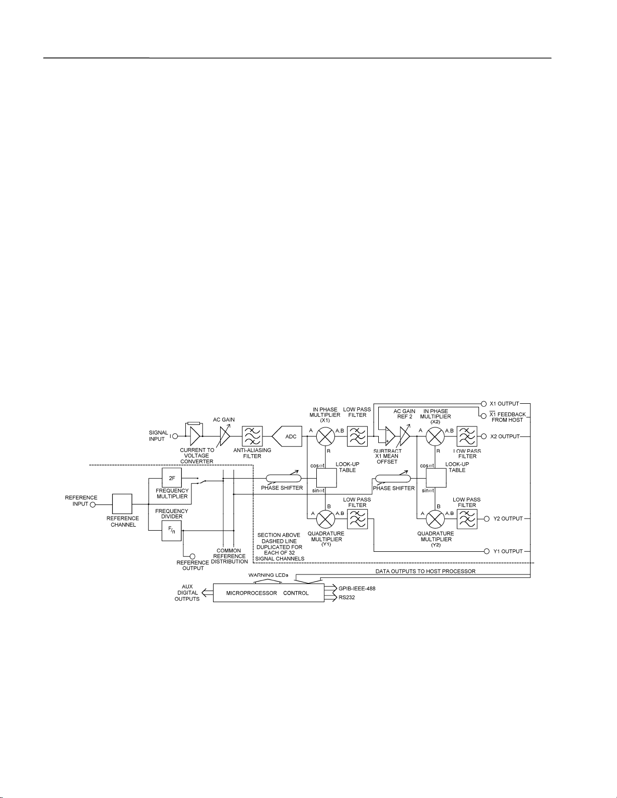
3.3.01 Block Diagram
The model 7210 uses 32 ADC's and digital signal processors (DSP's), a
microprocessor and very low-noise analog circuitry to achieve its specifications. A
block diagram of the instrument is shown in figure 3-1. The sections that follow
describe how each functional block operates and the effect it has on the instrument's
performance.
Figure 3-1, Model 7210 - Block Diagram

Chapter 3, TECHNICAL DESCRIPTION
3-3
3.3.02 Signal Channel Inputs
The signal input amplifier depends on the type of input signal boards fitted:
7210/99 Signal Board - Voltage Mode Inputs
In this case the input amplifier is a buffer stage with an input impedance of 10 MΩ.
The frequency response (-3 dB) extends from 20 Hz to 50.5 kHz
7210/98 Signal Board - Wide Bandwidth Current Mode Inputs
In this case the input amplifier is a single-ended current mode device with a fixed
transimpedance setting of 10E6 V/A. Hence an applied current of 1 µA will give a
1 V signal into the next stage. The frequency response (-3 dB) extends from 20 Hz to
50.5 kHz
7210/97 Signal Board - Low Noise Current Mode Inputs
In this case the input amplifier is a single-ended current mode device with a fixed
transimpedance setting of 10E7 V/A. Hence an applied current of 100 nA will give a
1 V signal into the next stage. The frequency response (-3 dB) extends from 20 Hz to
5.0 kHz.
3.3.03 AC Gain and Dynamic Reserve
The signal channel contains a number of analog filters and amplifiers whose overall
gain is defined by the AC Gain parameter, which is specified in terms of decibels
(dB). For each value of AC Gain there is a corresponding value of the INPUT LIMIT
parameter, which is the maximum instantaneous (peak) voltage or current that can be
applied to the input without causing input overload, as shown in table 3-1 below.
AC Gain (dB) INPUT LIMIT (V) INPUT LIMIT (nA) INPUT LIMIT (nA)
Voltage Mode Wide Bandwidth Low Noise
Current Mode Current Mode
0 3.1 3100 310
10 1.5 150 15
20 0.31 31 3.1
30 0.15 15 1.5
40 0.031 3.1 0.31
50 0.015 1.5 0.15
60 0.0031 0.31 0.031
Table 3-1, Input Limit vs AC Gain
It is a basic property of the digital signal processing (DSP) lock-in amplifier that the
best demodulator performance is obtained by presenting as large a signal as possible
to the main analog-to-digital converter (ADC). Therefore, in principle, the AC Gain
value should be made as large as possible without causing the signal channel
amplifier or converter to overload. This constraint is not too critical however and the
use of a value 10 or 20 dB below the optimum value makes little difference. Note that
as the AC Gain value is changed, the demodulator gain (described later in section
3.3.08) is also adjusted in order to maintain the selected full-scale sensitivity.
The full-scale sensitivity is set by a combination of AC Gain and demodulator gain.
Since the demodulator gain is entirely digital, changes in full-scale sensitivity which

Chapter 3, TECHNICAL DESCRIPTION
3-4
do not change the AC Gain do not cause any of the errors which might arise from a
change in the AC Gain.
The user is prevented from setting an illegal AC Gain value, i.e. one that would result
in overload on a full-scale input signal. Similarly, if the user selects a full-scale
sensitivity which causes the present AC Gain value to be illegal, the AC Gain will
change to the nearest legal value.
In practice, this system is very easy to operate. However, the user may prefer to make
use of the AUTOMATIC AC Gain feature which gives very good results in most
cases. When this is active the AC Gain is automatically controlled by the instrument,
which determines the optimum setting based on the full-scale sensitivity currently
being used.
At any given setting, the ratio
ySensitivitScale-Full LimitInput
0.7DR ×=
represents the factor by which the largest acceptable sinusoidal interference input
exceeds the full-scale sensitivity and is called the Dynamic Reserve of the lock-in
amplifier at that setting. (The factor 0.7 is a peak-to-rms conversion). The dynamic
reserve is often expressed in decibels, for which
))ratioalog(DR(as20dB)DR(in
×
=
Applying this formula to the model 7210 at the maximum value of INPUT LIMIT
and the smallest available value of FULL-SCALE SENSITIVITY, gives a maximum
available dynamic reserve of better than 80 dB.
3.3.04 Anti-Aliasing Filter
Prior to the main analog-to-digital converter (ADC) the signal passes through an anti-
aliasing filter to remove unwanted frequencies which would cause a spurious output
from the ADC due to the sampling process.
Consider the situation when the lock-in amplifier is measuring a sinusoidal signal of
frequency
f
signal
Hz, which is sampled by the main ADC at a sampling frequency
f
sampling
Hz. In order to ensure correct operation of the instrument the output values
representing the
f
signal
frequency must be uniquely generated by the signal to be
measured, and not by any other process.
However, if the input to the ADC has, in addition, an unwanted sinusoidal signal with
frequency
f
1
Hz, where
f
1
is greater than half the sampling frequency, then this will
appear in the output as a sampled-data sinusoid with frequency less than half the
sampling frequency,
f
alias
= |
f
1
- nf
sampling
|, where
n
is an integer. This alias signal is
indistinguishable from the output generated when a genuine signal at frequency
f
alias
is sampled. Hence if the frequency of the unwanted signal were such that the alias
signal frequency produced from it was close to, or equal to, that of the wanted signal
then it is clear that a spurious output would result.
Table of contents
Other Signal Recovery Amplifier manuals


