Silergy SY5802FAC 3 User manual
Evaluation Board SY5802FAC_3
Single Stage Flyback And PFC Controller
With Primary Side Control For LED Dimming
DB_SY5802FAC_3 Rev. 0.1 Silergy Corp. Confidential- Prepared for Customer Use Only 1
1. Introduction
The SY5802 is a single stage Flyback and PFC controller targeting at LED dimming applications. It is a
primary side controller without applying any secondary feedback circuit for low cost, and drives the Flyback
converter in the quasi-resonant mode to achieve higher efficiency. It keeps the Flyback converter in constant
on time operation to achieve high power factor.
2. Application
Provide 9W~12W output power and high power factor. It is compatible with 7 kinds of operation mode: No dimming,
Variable Resistor (VR) dimming (primary/secondary), 0-10V dimming (primary/secondary), PWM signal dimming
(primary/secondary)
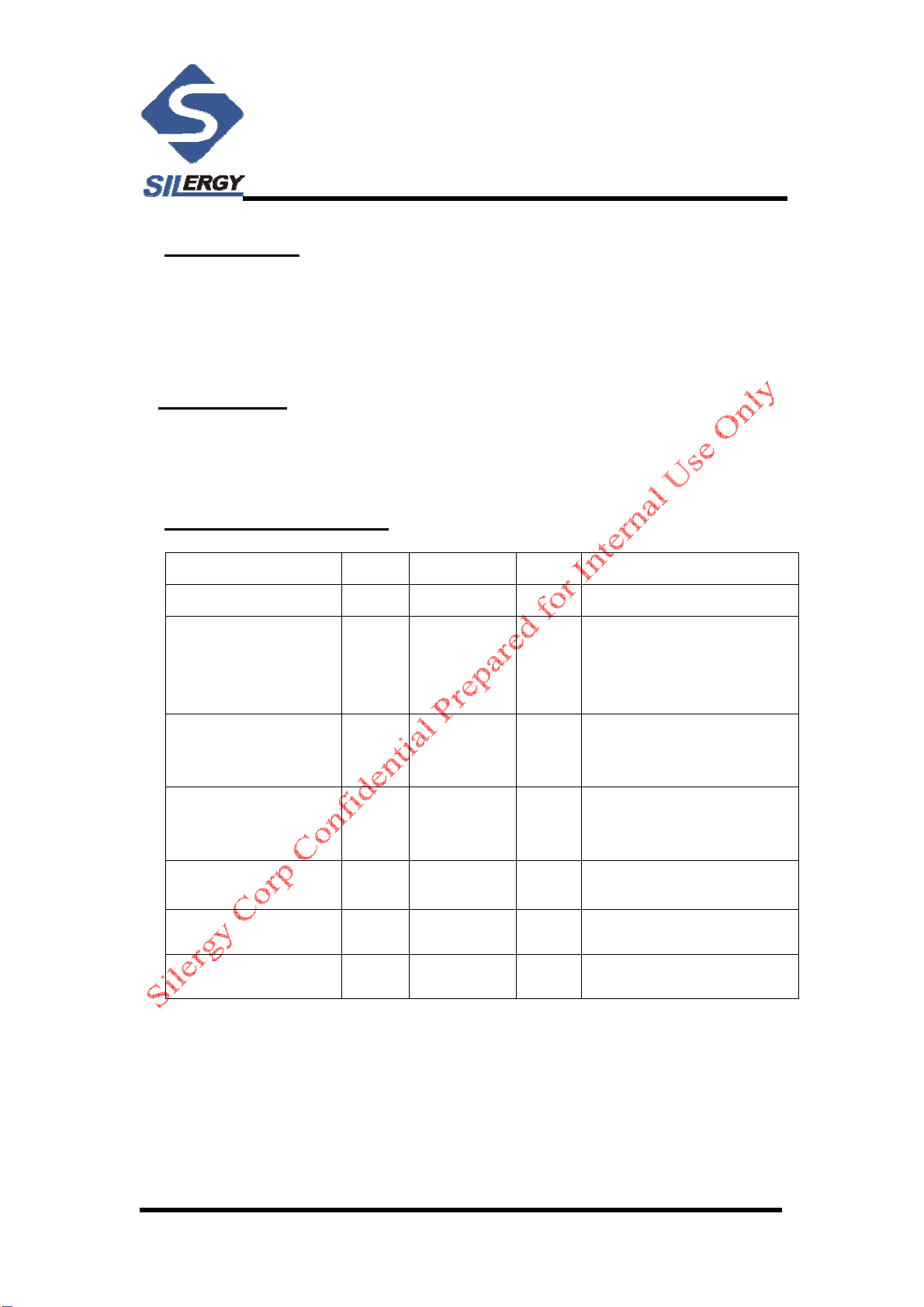
3. Design Specifications
Item Min Typical Max Note
Input Voltage(V) 90 100-240 264
Output
Voltage (V)
Current(mA)
Power(W)
30
36
300
10.8W
44
PF
(110Vac,full load)
(220Vac,full load)
>0.90
0.99
0.95
Efficiency
(110Vac,full load)
(220Vac,full load)
>84%
86.7%
86.4%
condition
Working temperature
-20℃
75℃
Dimming range 10% 100% When dimming operation
Standby Power 0.33W 0.4W 0.5W Vary with operation mode
DB_SY5802FAC_3
DB_SY5802FAC_3 Rev. 0.1 Silergy Corp. Confidential- Prepared for Customer Use Only 2
4. Application Guide
4.1 EVB structure
The evaluation board contains two sections: main board and dimming card:
Main board is a 9W~12W flyback converter controlled by SY5802 with two dimming interface (primary and
secondary port);
Dimming card is auxiliary circuit that transfer customer’s dimming signal to PWM waveforms. Two dimming
card (Variable Resistor dimming and 0-10V dimming) are already designed for customer.
4.2 Operation mode selection
For primary side dimming, dimming cards should be connected to primary side dimming port on main board;
for secondary side dimming, dimming cards should be connected to secondary side dimming port on main
board.
Dimming mode is up to the dimming card selected. For no-dimming mode, the dimming port on main board
is left floating; for PWM signal dimming, the dimming signal should be connected to the DIM1 or DIM2 pin
on main board directly.
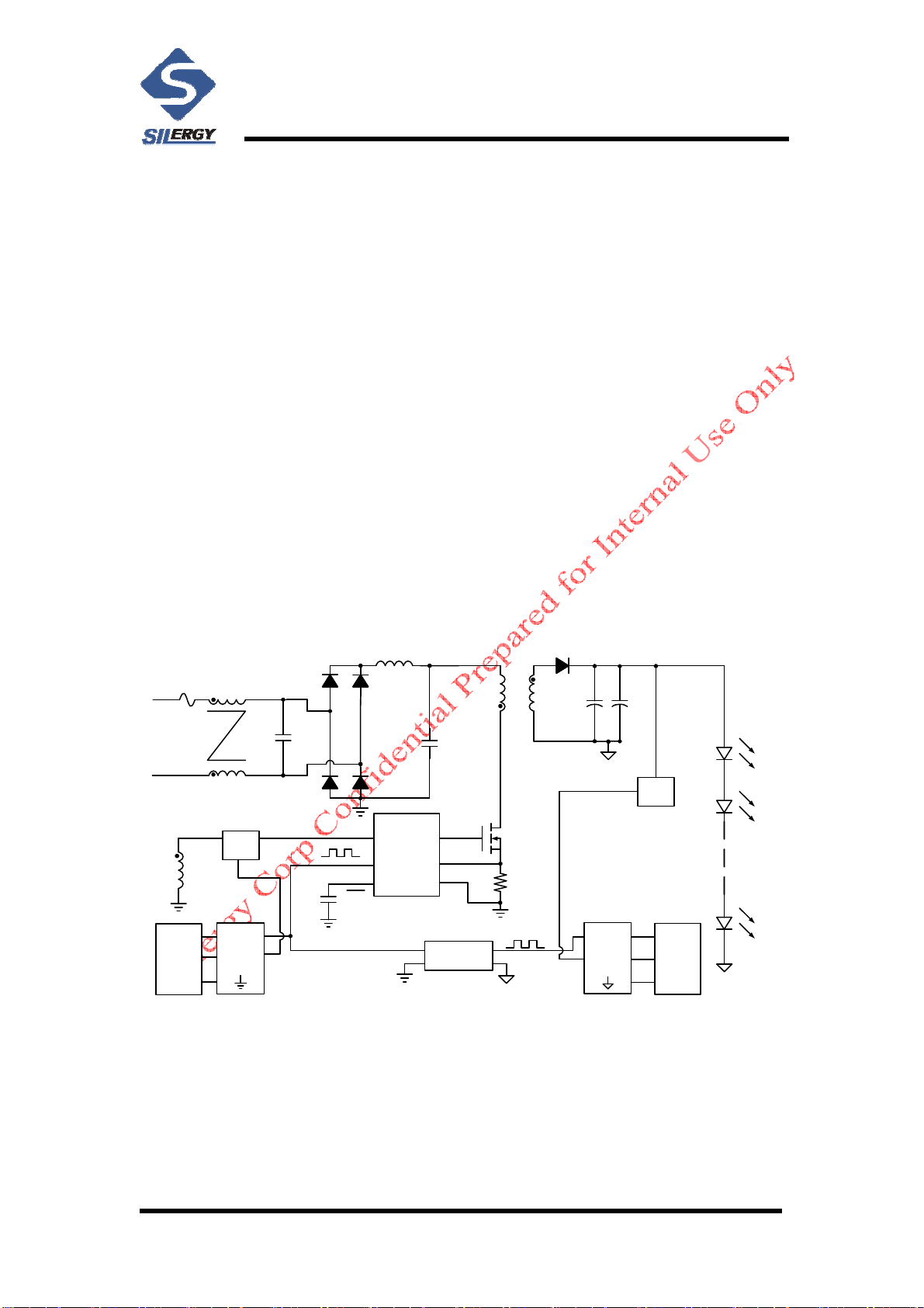
The structure circuit is shown in Fig.1.
T1
AC
source
LED
1
3
10
6
5
4
LDO
PWM
ADIM
1.5V x PWM Duty
Optoisolator
LDO
Dimming
PWM
Dimming
PWM
VIN GATE
VCC2
DIM2
Primary side
Dimming port
Dimming
card VCC1
DIM1
Second side
Dimming port
Dimming
card
ISEN
GND
SY5802
Fig.1 EVB structure circuit.

DB_SY5802FAC_3
DB_SY5802FAC_3 Rev. 0.1 Silergy Corp. Confidential- Prepared for Customer Use Only 3
5. Schematic
D3
D2
FR107
D1 MUR460
C5
100nF/400V
C1 2.2nF/250V
C3
220μF/63V
Q1
4N60
T1
R21
0.33
R13 10
D6
RS1M
AC
source
F1
C2
47nF/X2
L2
R10 10
R17
500
R24
1K
C13
1μF
C12
100pF
R25
12K
R8
1M
R9
1M
R1
100K LED
C11 1nF/Y1
R22
10
R2
5.1K
L1 1mH
R3
100K
1
3
10
6
5
4
C6
22μF/50V
R6
250k
Q2
U1
VIN
DRV
ADIM
ISEN
ZCS
COMP PWM
GND
SY5802
C10 2.2nF
ZD2 12V
C14
1μF
ZD1
12V
R5
50k
Q1
2N7002
R10
100k
R4
250K
C4
220μF/63V
C8 2μF
R26
100k
R12
2k
DIM1
Q2
2N7002
DIM2 U2
PC817
D4
BAV21
D5
BAV21
C15 2μF
R19 5k
R23 2k
R20 200k
D7 BAV21
R16 10 R18
100
VCC2
VCC1
VCC1
DIM1
Second side
Dimming port
Dimming
card
VCC2
DIM2
Primary side
Dimming port
Dimming
card
Fig.2 Main board Schematic Diagram
THR
CVOLT
DIS
OUT
TRIG
GND VCC
RST
NE555 12V VCC
12V VCC
R3
R4
D1 D2
C2 C3
VCC
DIM
R2
Dimming
port
VR
Fig.3 Variable Resistor (VR) Dimming card Schematic Diagram
+
-
12V
VCC
12V
VCC
+
-
Dimming
signal
12V
VCC
C2
R6
R8
R3
R4
R7
R2
LM393
LM
393 VCC
DIM
12V VCC
R5
R9
Dimming
port
Fig.4 0~10V Dimming card Schematic Diagram
DB_SY5802FAC_3
DB_SY5802FAC_3 Rev. 0.1 Silergy Corp. Confidential- Prepared for Customer Use Only 4
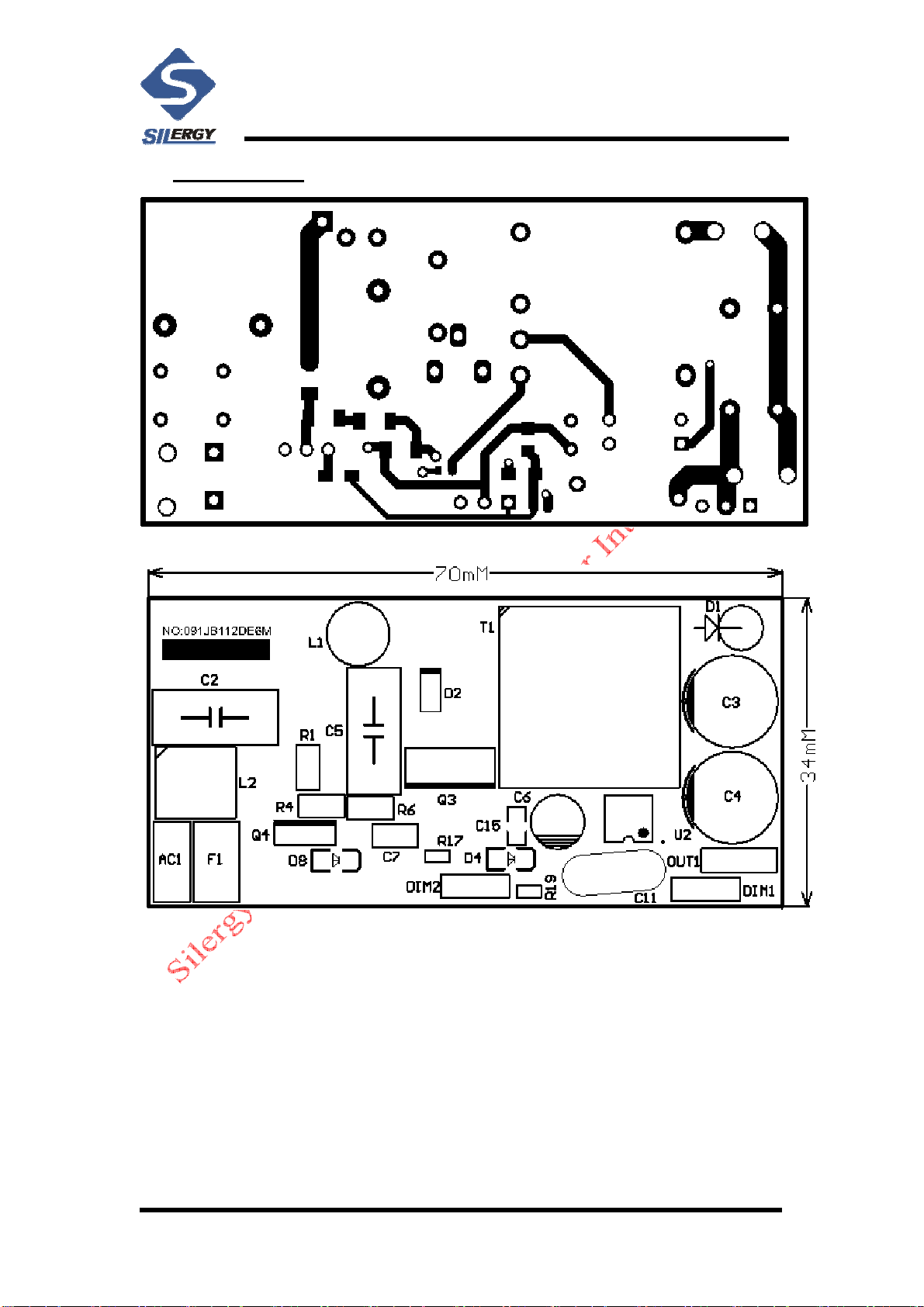
6. PCB Layout
(a)Top layer
(b) Top layer Silkscreen
Fig.5 Main board top view

DB_SY5802FAC_3
DB_SY5802FAC_3 Rev. 0.1 Silergy Corp. Confidential- Prepared for Customer Use Only 5
(a) Bottom layer
(b) Bottom layer Silkscreen
Fig.6 Main board bottom view
(a)Toplayer (b)ToplayerSilkscreen
Fig.7 0~10V Dimming Card top view

DB_SY5802FAC_3
DB_SY5802FAC_3 Rev. 0.1 Silergy Corp. Confidential- Prepared for Customer Use Only 6
(a) Bottom layer (b) Bottom layer Silkscreen
Fig.8 0~10V Dimming Card bottom view
(a)Toplayer (b)ToplayerSilkscreen
Fig.9 Variable Resistor Dimming Card top view
(a) Bottom layer (b) Bottom layer Silkscreen
Fig.10 Variable Resistor Dimming Card bottom view

DB_SY5802FAC_3
DB_SY5802FAC_3 Rev. 0.1 Silergy Corp. Confidential- Prepared for Customer Use Only 7
7. BOM List
Main board Bom list
Reference Designator Description Note
C1 2.2nF/630V/1206 GRM31BR72J222KW01L by muRata
C10 2.2nF/0603 C1608C0G1H222J by TDK
C11 1nF/Y2
C12 100pF/0603
C1608C0G1H100D by TDK
C13, C14 1μF/25V/0603 C1608X5R1E105K by TDK
C2 47nF/250VAC
C3, C4 220μF/63V
C5 100nF/400V
C6 22μF/50V
C7 22μF/25V/1206 C3216X5R1C226K by TDK
C8, C15 2.2μF/50V/0805 C2012Y5V1H225Z by TDK
C9 NC
R1, R3 100K/1206
R10, R26 100k/0603
R11, R18 10K/0603
R12 2K/0805
R13 10/0805
R16 100/0805
R17 500K/0603
R19 5K/0603
R2 5.1K/0805
R20 200K/0603
R21 0.33/1206
R23 2K/0603
R24 1K/0603
R25 13.7K/0603
R4, R6 250K/1206
R5 51k/0603
R7, R8 1M/1206
R14, R15 NC
R9, R22 10/1206
U2 PC817C
U1 SY5802
ZD1, ZD2 12V/LL34
DB_SY5802FAC_3
DB_SY5802FAC_3 Rev. 0.1 Silergy Corp. Confidential- Prepared for Customer Use Only 8
ZD3 NC
DIM1, DIM2
F1 250VAC/1A
L1 1.5mH Φ6
L2 20mH EE8.3
D1 MUR460 DO-267
D2 1N4007 DO-41
D3 DB107 DB-1
D4, D5, D7, BAV21W SOD123
D6 RS1M DO214AC
D8 NC
Q3 4N60C TO220
Q4 NC
Q1,Q2,Q5 2N7002 SOT23
T1 700μH/EFD20 Manufactured by 鑫源洋
0~10V Dimming card bom list
Reference Designator Description Note
U1 LM393
R2,R4 2K/0603
R3 10K/0603
R5 100/0603
R6,R8,R9 100K/0603
R7 5K/0805
C2 220pF/0603 C1608C0G1H221J by TDK
Variable Resistor Dimming card bom list
Reference Designator Description Note
U1 NE555
RES1 100K TYPE 09
R2 100/0603
R3,R4 10K/0603
D1,D2 BAV21W SOD123
C2,C3 1nF/0603 C1608C0G1H102J by TDK
DB_SY5802FAC_3
DB_SY5802FAC_3 Rev. 0.1 Silergy Corp. Confidential- Prepared for Customer Use Only 9
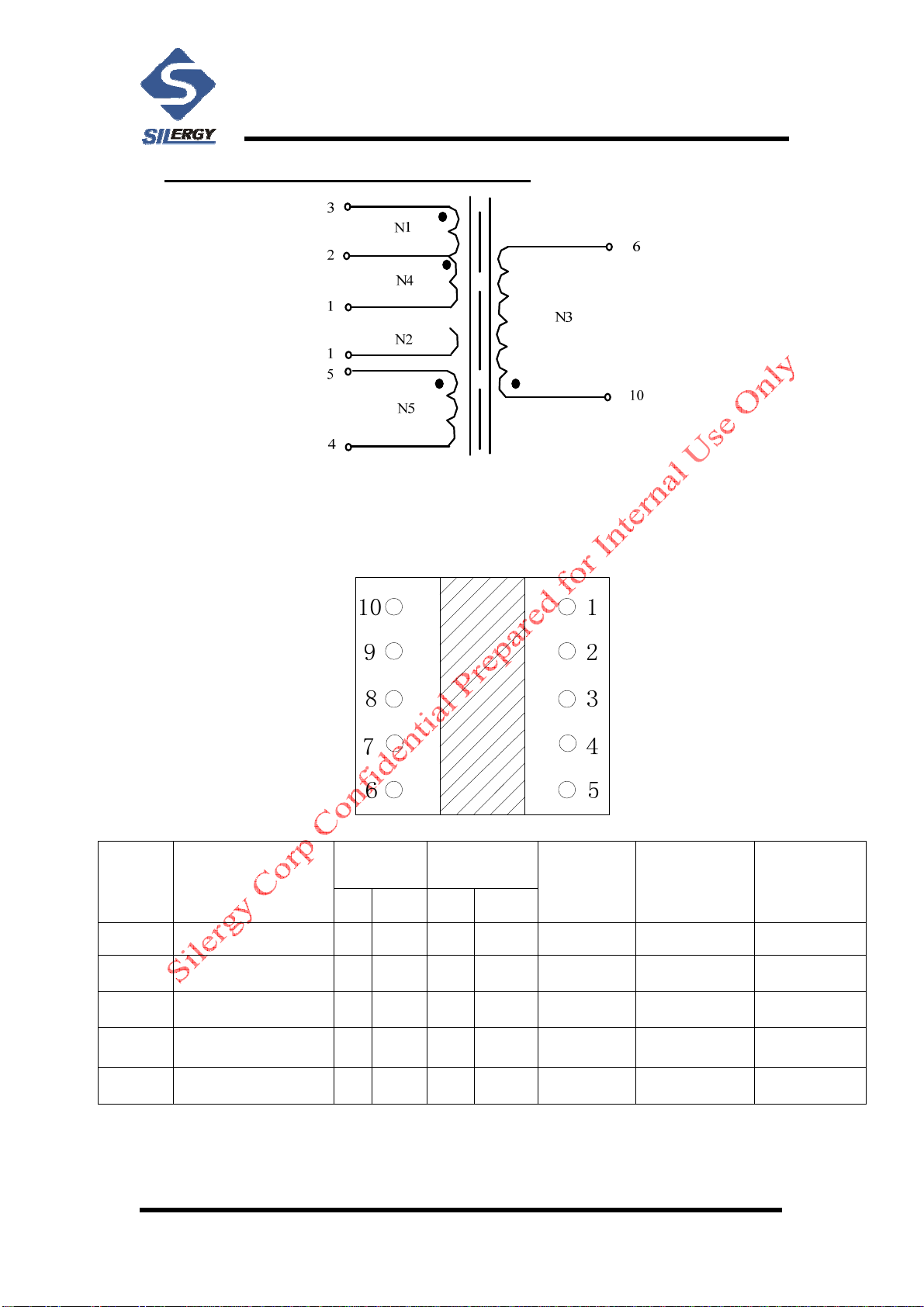
8. Transformer Design Specifications
Temperature:25±5℃ Humidity:65±25%
Test Condition:40 KHz, 1V
L:PIN (1-3) =700μH±5%
LK:PIN (1-3) =10μH/MAX,(SHORT SEC)
Bottom overview (EFD20 core with air gap)
Winding Wire diameter*Number
Pin PTFE tube
TS Insulating Tape
9.5mm(TS) Notes
IN OUT IN OUT
N1 Ø0.25*1(2UEW) 3 2 46 2 Close wound
N2 Ø0.15*1(2UEW) 1 70 2 Close wound
N3 Ø0.35*1(TEX-E) 10 6 46 2 Close wound
N4 Ø0.25*1(2UEW) 2 1 46 2 Close wound
N5 Ø0.19*1(2UEW) 5 4 46 2 Close wound

DB_SY5802FAC_3
DB_SY5802FAC_3 Rev. 0.1 Silergy Corp. Confidential- Prepared for Customer Use Only 10
Start(Pin 3)
End (Pin 2)
Start
(Pin 10)
End
(Pin 6)
Start(Pin 2)
End (Pin 1)
Start(Pin 5)
End (Pin 4)
Start(Pin 1)
Transformer Structure
9. Quick Start Guide
1. Connect the input supply to L and N input connectors.
2. Connect the LED load between LED+ and LED- output connectors.
3. Preset the input supply to a voltage between 85V and 264Vac.
4. Connect Dimming card for different dimming application
Primary side Dimming Port + VR Dimming card = Primary side VR Dimming
Secondary side Dimming Port + VR Dimming card = Secondary side VR Dimming
Primary side Dimming Port + 0~10V Dimming card = Primary side 0~10V Dimming
Secondary side Dimming Port + 0~10V Dimming card = Secondary side 0~10V Dimming
5. Turn on the input supply and measure the LED Current.

DB_SY5802FAC_3
DB_SY5802FAC_3 Rev. 0.1 Silergy Corp. Confidential- Prepared for Customer Use Only 11
10. Operation Performances
10.1 Steady States – No dimming
10.2 Output Ripple – No dimming
10.3 Start Up & Shut Down – No dimming
Startup
Time (20ms/div)
(VIN=110V(AC), Full Load)
VOUT 20V/div
IOUT 0.2A/div
VDrain 100V/div
Shutdown
Time (20ms/div)
(VIN=110V(AC), Full Load)
VDrain 100V/div
VDrain 100V/div
IOUT 0.2A/div
VOUT 20V/div
VDrain 100V/div
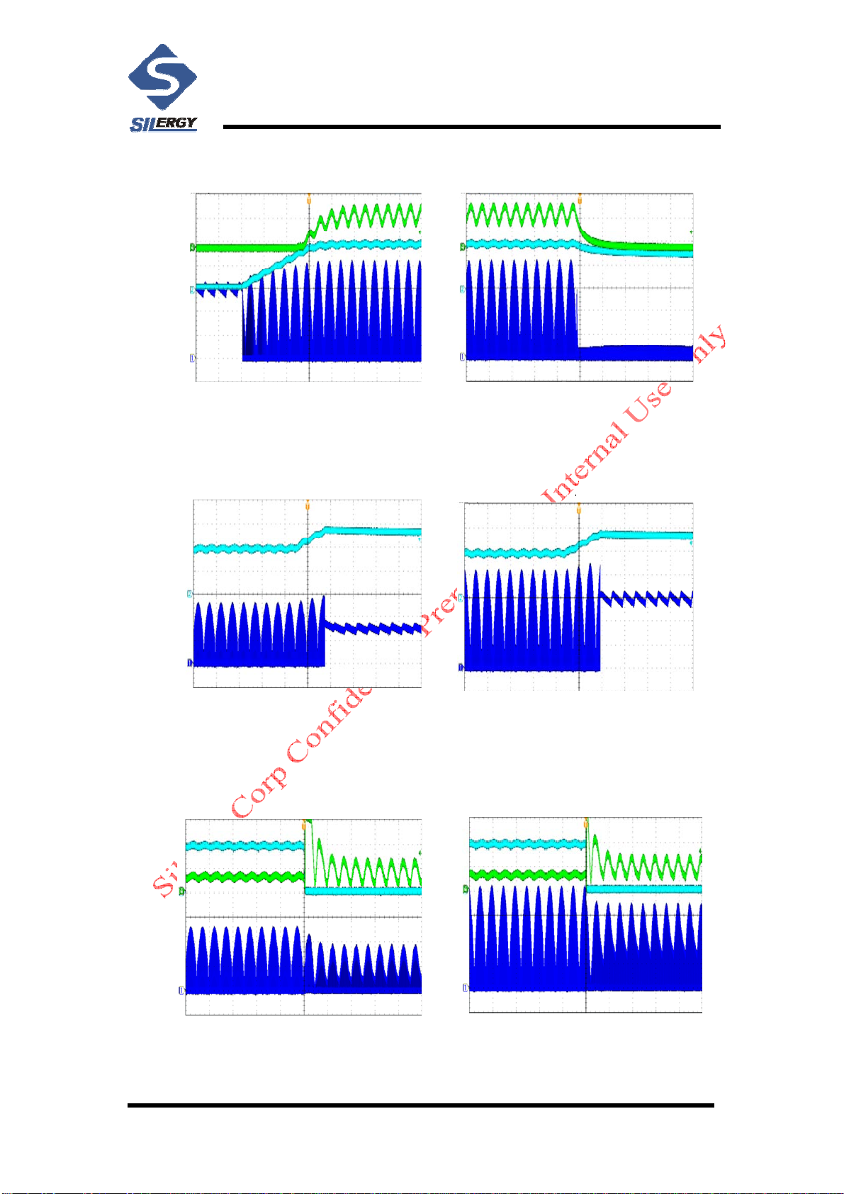
DB_SY5802FAC_3
DB_SY5802FAC_3 Rev. 0.1 Silergy Corp. Confidential- Prepared for Customer Use Only 12
Startup
Time (20ms/div)
(VIN=220V(AC), Full Load)
IOUT 0.2A/div VOUT 20V/div
VDrain 100V/div
Shutdown
Time (20ms/div)
(VIN=220V(AC), Full Load)
VDRAIN 100V/div
VDrain 100V/div
IOUT 0.2A/div IOUT 0.2A/div
VDrain 100V/div
10.4 Open LED Protection – No dimming
Open LED Protection
Time (20ms/div)
(VIN=110V(AC))
VDrain 100V/div
VDrain 100V/div
VOUT 20V/div
Open LED Protection
Time (20ms/div)
(VIN=220V(AC))
VOUT 20V/div
VDrain 100V/div
10.5 Short Circuit Protection – No dimming
Short Circuit Protection
Time (20ms/div)
(VIN=110V(AC))
VOUT 20V/div
IOUT 1A/div
VDrain 100V/div
Short Circuit Protection
Time (20ms/div)
(VIN=220V(AC))
VOUT 20V/div
IOUT 1A/div
VDrain 100V/div

DB_SY5802FAC_3
DB_SY5802FAC_3 Rev. 0.1 Silergy Corp. Confidential- Prepared for Customer Use Only 13
10.6 Line Transient – No dimming
Line Transient
Time (20ms/div)
(VIN=85V-132V)
IOUT 0.1A/div
Line Transient
Time (20ms/div)
(VIN=132V-85V)
IOUT 0.1A/div
DB_SY5802FAC_3
DB_SY5802FAC_3 Rev. 0.1 Silergy Corp. Confidential- Prepared for Customer Use Only 14
10.7 Efficiency
Input Voltage(VAC)
265
Efficiency vs.Input voltage(VAC)
84
84.5
85
85.5
86
86.5
87
87.5
90 115 140 165 190 215 240
No Dimming
Primary Side VR Dimming
Second Side VR Dimming
Primary Side 0~10V Dimming
Second Side 0~10V Dimming
10.8 Dimming Efficiency
Efficiency vs.Input voltage(VAC)
Input Voltage(VAC)
265
65
70
75
80
85
90
90 115 140 165 190 215 240
Second Side 0-10V Dimming 100% Output
Second Side 0-10V Dimming 75% Output
Second Side 0-10V Dimming 50% Output
Second Side 0-10V Dimming 25% Output
10.9 Line Regulation
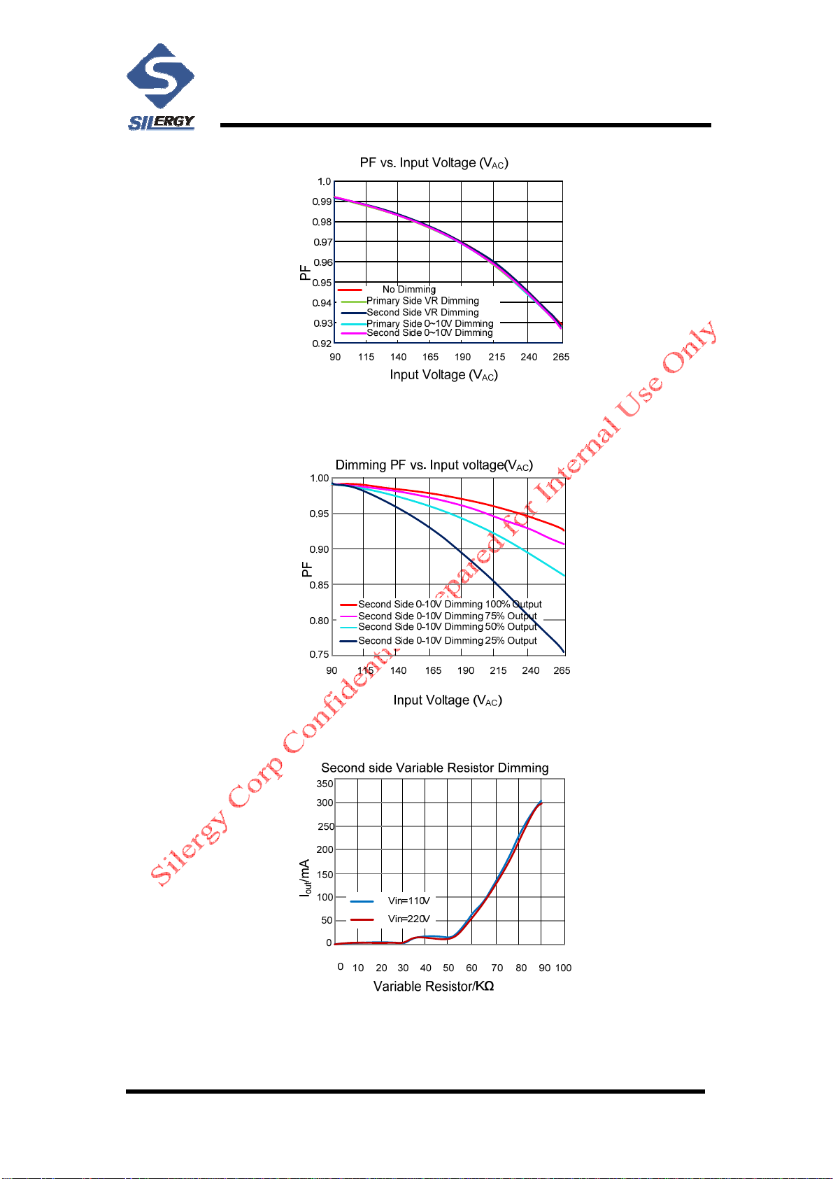
10.10 Power Factor
DB_SY5802FAC_3
DB_SY5802FAC_3 Rev. 0.1 Silergy Corp. Confidential- Prepared for Customer Use Only 15
10.11 Dimming Power Factor
10.12 Second side Variable Resistor Dimming curve

DB_SY5802FAC_3
DB_SY5802FAC_3 Rev. 0.1 Silergy Corp. Confidential- Prepared for Customer Use Only 16
10.13 Primary side Variable Resistor Dimming curve
10.14 Second side 0~10V Dimming curve
10.15 Primary side 0~10V Dimming curve
Table of contents


