Sixty Four Pixels PCLONE2 User manual

PCLONE2 –Analog Percussion Synthesizer
Welcome to the PCLONE2 build instructions!
I’ll assume you’ve done some soldering before and skip the basics,
however if you do need some tips or reminders on soldering technique,
please check out my page here. As kits go, this is moderate in complexity.
You should give yourself at least 3-4 hours to make the kit and go slowly
and carefully –it is much easier to avoid a mistake than fix it afterwards…
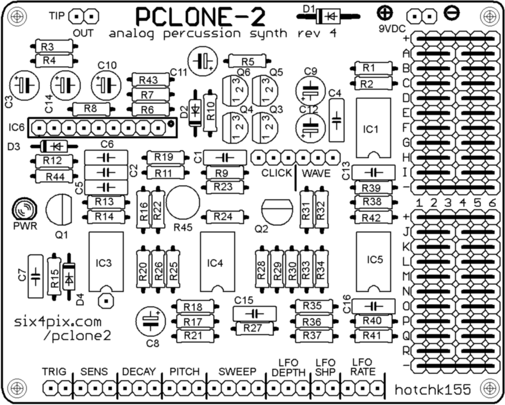
Here is an image of the main PCB layout which can be useful to refer to as
you work, especially if you accidentally put a component in the wrong
place, covering up the designator (Click here for a bigger version)

OK, Let’s begin by soldering the resistors. The different resistors can be
identified by their coloured stripes, which are listed in the table below (when
reading the resistor codes you can ignore the silver or gold “tolerance
band”)
The body of the resistor may be a tan or blue colour depending on the type
(carbon or metal film). The body colour doesn’t matter, so don’t worry if the
colour does not match the photo.
Designators on PCB
Value
Colour Code
R37
330
ORANGE-ORANGE-BROWN
R6, R7, R17, R21
1k
BROWN-BLACK-RED
R14, R20, R22, R44
4k7
YELLOW-VIOLET-RED
R15
10k
BROWN-BLACK-ORANGE
R13, R26, R27, R39,
R43
22k
RED-RED-ORANGE
R8, R19
33k
ORANGE-ORANGE-ORANGE

R1, R2, R4, R5, R23,
R28, R29, R33, R34,
R38, R41, R42
47k
YELLOW-VIOLET-ORANGE
R18
56k
GREEN-BLUE-ORANGE
R9, R11, R12, R24, R25,
R30, R31, R35, R36,
R40
100k
BROWN-BLACK-YELLOW
R32
220k
RED-RED-YELLOW
R10
1M
BROWN-BLACK-GREEN
R16
4M7
YELLOW-VIOLET-GREEN
Note: The space for R3 is not populated. The kit does contain spare
resistors and some extras of certain useful values for mods, so don’t be
confused if there seem to be too many of a particular value, and don’t throw
away the leftovers!
The board should look like this:

Now let’s fit the diodes, remembering that they need to be soldered the
correct way around (and don’t heat them for too long when soldering)
•D2, D3 and D4 are small signal diodes with a small orange glass
body with a black stripe. Make sure the black stripe lines up with
the stripe marked on the circuit board symbol.
•D1 is a larger rectifier diode with a black body and silver stripe.
Make sure the stripe matches up with the one printed on the
board.
Your board should now look something like this

Now let’s solder the four, 8-pin IC sockets and the 9-pin header strip.
Take care to align the notch on the end of the 8 pin sockets with the
marking on the board. In this layout the notch is towards the bottom of the
board for each socket.
With all the sockets in place the board should be looking like this

The next step is to insert the nine polyester box capacitors.
Designators on PCB
Value
Markings
C1, C2, C6
47nF
“47n”
C13
22nF
“22n”
C16
3.3nF
“3n3”
C4, C5, C7, C15
1nF
“1n”
The markings will contain other codes (e.g. “47nK100”), but check they
start with the indicated value (e.g. “47n”)
With these caps fitted, the board now looks like this

Now insert the trimmer potentiometer, R45. This is pretty tight to insert into
the PCB and may need a bit of waggling –be careful not to damage the
legs.
Solder the LED. It is important that this goes the right way around; you’ll
see that the marking on the board shows a “flat” side next to one of the legs
(beside the “PWR” label). The LED has a matching “flat” (marking the
negative terminal, which also has a shorter leg). Line the flats up when
inserting the LED and don’t heat for too long when soldering.

Now for transistors. There are three types of transistor in the kit
Designators on PCB
Type
Notes
Q1, Q2
2SC945P
NPN (Marked “945P” or
“C945”)
Q3, Q4
2N3906
PNP
Q5, Q6
2N3904
NPN
It is very important not to mix them up (or you might let the magic smoke
out of them as soon as you apply power!). There is an extra 2N3904 in the
kit –hang on to it to use for mods…
When you solder them, make sure the “D” shape of the case lines up with
the D shaped marking on the board –you need to bend or splay the legs a
little to get them into the holes on the board. When soldered, the transistors
should sit above the board by a few millimetres.

Now add the electrolytic capacitors. These need to go in the right way
around. The symbols on the circuit board show a tiny little (+) sign next to
one hole. Put the longer leg of the capacitor through the hole. The
capacitor body will also have a white stripe to mark the negative terminal
(aligned with the shorter leg)
As with the box capacitors they are easy to mix up, so pay special attention
to the markings
C3, C11, C12
1uF/50V
C8
2.2uF/50V
C9
10uF/16V
C10, C14
100uF/16V

Make sure you trim back the excess component legs on the underside of
the board, since the back of the board will be mounted close to the metal
bodies of the potentiometers.
The rear of the board should look a bit like this

Almost there! The next step is to add the sockets that will join the main
PCB to the control panel PCB.
Start by inserting the longer 23-pin header through its holes. Note that the
headers are attached to the underside of the PCB as shown in the
photo.
It can help to stand the board on the header while soldering (support the
other edge of the board so that the header is perpendicular to the board.
Repeat this process for the 6-pin female header, being careful not to
damage the nearby components with the soldering iron!

Now let’s insert the ICs.
IC1
RC4558
Op-amp DIP8
IC3, IC4, IC5
LM2904
Op-amp DIP8
IC6
BA6110
Op amp SIL9 –9 pins in a single
row
For IC1, IC3, IC4, IC5, make sure that the notch or dimple on the body of
the chip matches the notch shown in the symbol on the board (which
should also match the notch on the socket). The location for each notch is
toward the bottom edge of the board.

For IC6, there is a notch along the top of the chip. This should be towards
the right (There is a dot marked on the board).
A firm push is needed to insert IC6 but take special care not to bend of
break any legs –These are old chips (no longer manufactured) and your
chip may have been recovered from other equipment, so the legs can be a
bit more fragile than the other ICs.

And so, on to the front panel…
Locate the front panel PCB and ensure that the pre-soldered connectors on
the front panel are undamaged.
Locate the acrylic case front panel and remove all the protective film

Locate the piezo disk and adhesive pads
Place the front panel over the PCB so that all the holes line up and the
large round cut out is on the right side (and the PCB connectors are on the
opposite side)
Stick half of one of the pads to the PCB in the centre of the circular cut-out.
Stack another half pad on top so the pad is double thickness.

Stick the piezo disk to the pad in the centre of the cut out so that it fits
inside the cut out space and the piezo wires lead off to the left (9 o’clock
position)

Carefully slide the acrylic panel along the wires, being sure not to break the
connection to the piezo disk. The PCB should now look like this…
Remove all the nuts and washers from the potentiometers:

Locate the 470R potentiometer and use pliers to carefully bend the legs of
the potentiometer upwards (in the same direction as the spindle) as shown
below
Place the 470R potentiometer through the “sweep” position and attach the
washer and nut to the front side and tighten the nut

Use a generous amount of solder to attach the legs of the potentiometer to
the solder pads on the PCB. A wide roll of tape makes a good support for
the board during this process.

Repeat this process for all six potentiometers. I recommend you work
through them in the order of the following table for best access during
soldering:
470R LIN
Sweep
1M LOG
Decay
100K LOG
Rate
100K LOG
Sensitivity
100K LOG
Depth
100K LOG
Pitch
The end result should look like this
Other Sixty Four Pixels Synthesizer manuals


 Build guide")


