SECTION 2
1C FUNCTION DESCRIPTION SECTION 3
DISSASSEMBLY OF BASE UNIT
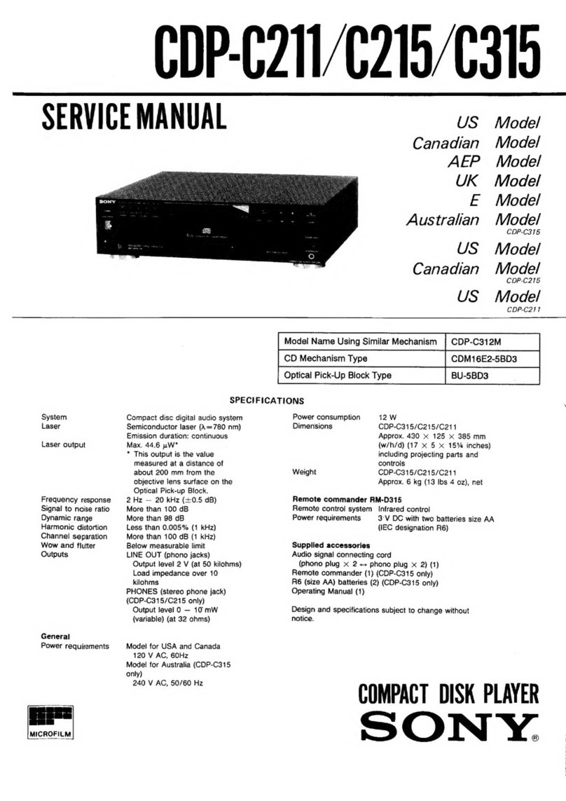
IC101 (CXA1372Q) PIN DESIGNATION
Pin No. Pin Name I/O Pin Description
1VC GND when two (±) dual power supplies are in use, or the center voltage (2.5 V)
when asingle power supply is in use.
2FGD ITime constants for gain switching in normal mode/down mode and for focus gain are
3FS3 Iconnected between the FGD and FS3 pins.
4FLB IThe capacitor for low frequency boost in the focus servo loop is connected.
5FEO 0Focus drive output
6FE —IInverted input to focus amplifier
7SRCH ITime constants to generate the focus search waveform are connected.
8TGU ITime constants for gain switching in normal mode/up mode and for tracking gain are
9TG2 Iconnected between TGU pin and TG2 pin.
10 AVCC Analog power supply (5 Vwhen ±dual power supplies are in use, 5Vwhen asingle
power supply is in use.)
11 TAO 0Tracking drive output
12 TA- IInverted input to tracking amplifier
13 SL +INon- inverted input to sled amplifier
14 SLO 0Sled drive output
15 SL -INon-inverted input to sled amplifier
16 ESET IThe 610- kQ phase compensator resistor is connected to this pin.
17 ISET IThe current setting resistor is connected to this pin.
18 SSTOP IThe limit switch is connected to this pin.
19 AVEE Analog power supply (-5V when ±dual power supplies are in use, or GND when asingle
power supply is in use.)
20 DIRC IDirect control pin.
21 LOCK ISled run- away prevention circuit operates when this signal is “L".
22 CLK ISerial data transfer clock input that is supplied from CPU (or DSP).
23 XLT ILatch input from CPU (or DSP).
24 DATA ISerial data input from CPU (or DSP).
25 XRST ISystem reset. "V to reset.
26 C.OUT 0Output to tracking counter.
27 SENS 0SENS output
28 DGND Digital ground (GND). (GND when ±dual power supplies are in use. GND when asingle
power supply is in use.)
29 MIRR 0Mirror output.
30 DFCT 0Defect output. *TT when defective.
31 ASY IAuto-assymmetry control input.
32 EFM 0EFM comparator output.
33 FOK 0Focus OK
34 CC2 IDefect- bottom- hold input (input by capacitive coupling).
35 CC1 0Defect-bottom -hold output
36 DVCC Digital power supply (+5 Vwhen ±dual power supplies in use. +5 Vwhen asingle
power supply is in use.)
37 CB IThe defect- bottom- hold capacitor is connected to this pin.
38 CP IThe mirror hold capacitor is connected to this pin.
39 RF1 IRF signal input (input by capacitive coupling).
40 RFO IRF signal input (input by DC coupling).
41 DVEE Digital power supply (-5 Vwhen ±dual power supplis are in use. GND when asingle
power supply is in use.)
42 TZC ITracking zero cross comparator input.
43 TE ITracking error input.
44 TDFCT IThe defect prevention hold capacitor is connected to this pin.
45 ATSC IAnti-shock input.
46 FZC IFocus zero- cross comparator input.
47 FE IFocus error input.
48 FDFCT IThe defect prevention hold capacitor is connected to this pin.
Note:
Follow the disassembly procedure in the nomerical
order given.
OTurn the cam to the direction of arrow (Counter
clock wise) by minus screw driver.
QTake off the disc table.
©Remove the bracket yoke.
©Remove the MD (BU-5BD1) to the direction of arrow.
ELECT
1. Perfo
2. Use 1
wise
3. Use t
RF LE
This
Optical
Procedr
1. Conn
TP f
2. Turn
3. Put t
4. Confi
Optir
clear
RF L
E-F Bi
This
Optical
Procedi
1. Conr
and '
2. Grot
3. Turr
-5- -6-

