SOtM sMB-Q370 User manual

sMB-Q370 embedded Motherboard
Product Guide
www.sotm-audio.com
Rev 1.1c

1
Motherboard Spec
sMB-Q370
Micro-ATX Form Factor
Intel® Coffee Lake Processor with Q370 Chipset
MECHANICAL
FORM FACTOR
Micro-ATX: 9.6” x 9.6” (244 mm x 244 mm)
SYSTEM
PROCESSOR
Support for 9th and 8th Generation Intel® CoreTM processors,
Intel® Pentium® processors, and Intel® Celeron® processors
(up to 95 W TDP)
CHIPSET
Intel®Q370 (Support RAID 0 / 1 / 5 / 10)
(optional external clock input)
MEMORY
DDR4 2666MHz, 4 x 288-pin DIMM, Max. 64GB (Non-ECC)
GRAPHICS
Intel®HD Graphics
ETHERNET
Realtek RTL8111HS Gigabit LAN controller
(optional external clock input)
AUDIO
ALC892 (optional)
TPM
2x8 pin TPM header
EXPANSION
SLOT
PCI-E 3.0 x16 slot
PCI-E Gen.3 x4 slot
PCI-E Gen.3 x1 slot
2x M.2 M key 2280 (PCI-E x4)
2x M.2 E key 2230 (PCI-E x2, USB)
BIOS
256 Mbit SPI, AMI BIOS
H/W MONITOR
Temperature Monitor, Voltage Monitor, Fan Monitor
WATCHDOG
TIMER
1~255 Steps by Software Program
SMART FAN
CONTROL
CPU Fan / System Fan
GRAPHICS
HDMI
Up to 4K (4096 x 2160) @30 Hz
DISPLAYPORT
Up to 4K (4096 x 2304) @60 Hz
eDP
Up to 4K (4096 x 2304) @60 Hz
LVDS(Optional)
Up to 1920 x 1200 @60 Hz
DVI, VGA
—

2
REAR I/O
USB
4 x USB 3.1 Gen. 2 (up to 10 Gbps), 2 x USB 2.0
DISPLAY I/O
1 x DisplayPort, 1 x HDMI
LAN I/O
1 x RJ-45
AUDIO I/O
—
INTERNAL CONNECTORS
STORAGE
6 x SATA 6Gb/s
USB
4 x USB 2.0, 2 x USB 3.1 Gen.2
DISPLAY I/O
LVDS connector (colay eDP connector), Panel power Header
(default 5V, option to 12V, 3.3V),
panel backlight power setting header (default 12V),
LVDS inverter power header
AUDIO I/O
1 x 10-pin box header(optional)
SERIAL PORT
2 x 10-pin UART 3.3V TTL level(optional)
FAN
1 x 4-pin CPU Fan Connector, 1 x 4-pin System Fan Connector
POWER
1 x 8-pin ATX Power Connector, 1 x 24-pin ATX Power
Connector, 1 x AT / ATX Mode Select Jumper
OTHERS
U.FL external clock input connector for the system and Ethernet
1 x clear CMOS jumper
POWER REQUIREMENT
POWER INPUT
12V CPU ATX Power Connector + ATX 24-pin
ENVIRONMENTAL
OPERATING
TEMPERATURE
0 ~ 55°C (32 ~131°F)
STORAGE
TEMPERATURE
-20 ~ 70°C (-4 ~158°F)
OPERATING
HUMIDITY
10% ~ 95% R / H, non-condensing
CERTIFICATION
CE & FCC Class B, KC
OS
OS SUPPORT
Windows®10 64-bit 1809 LTSC
Linux (customer provide version and kernel version)
PACKING LIST
PACKAGE
1 x Motherboard, 2 x SATA Cable, 1 x I/O Shield,
1 x Quick Guide
3
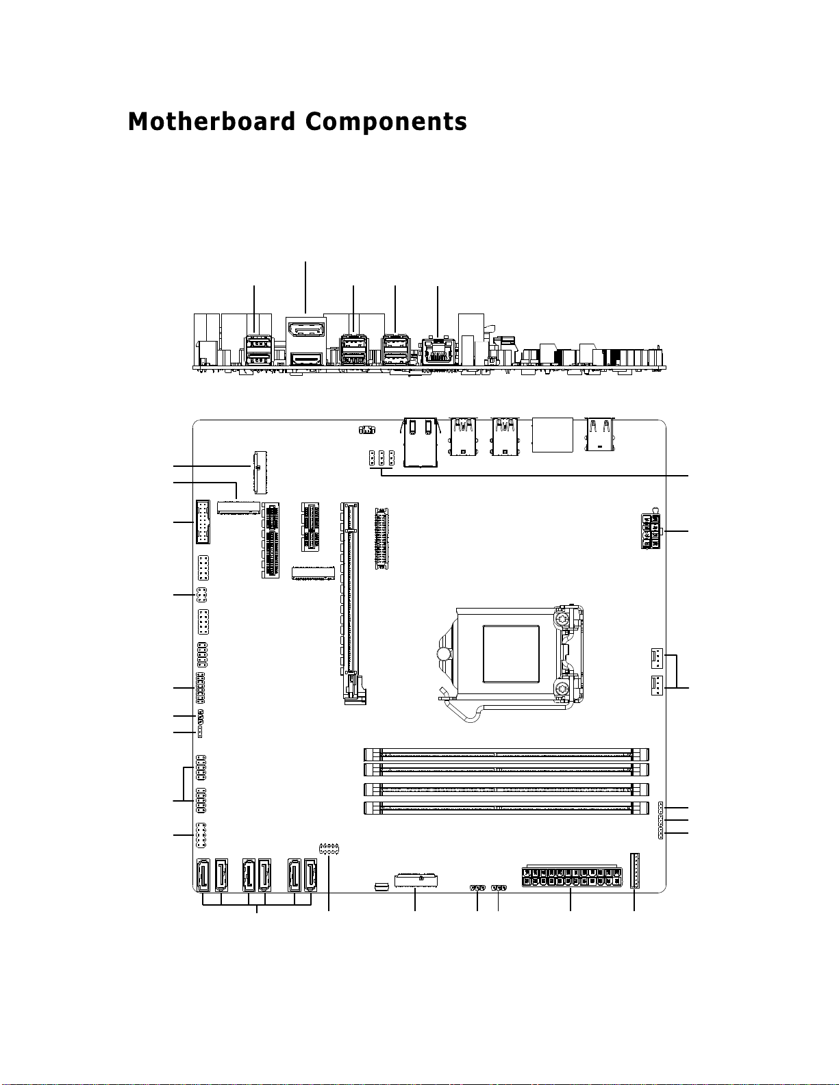
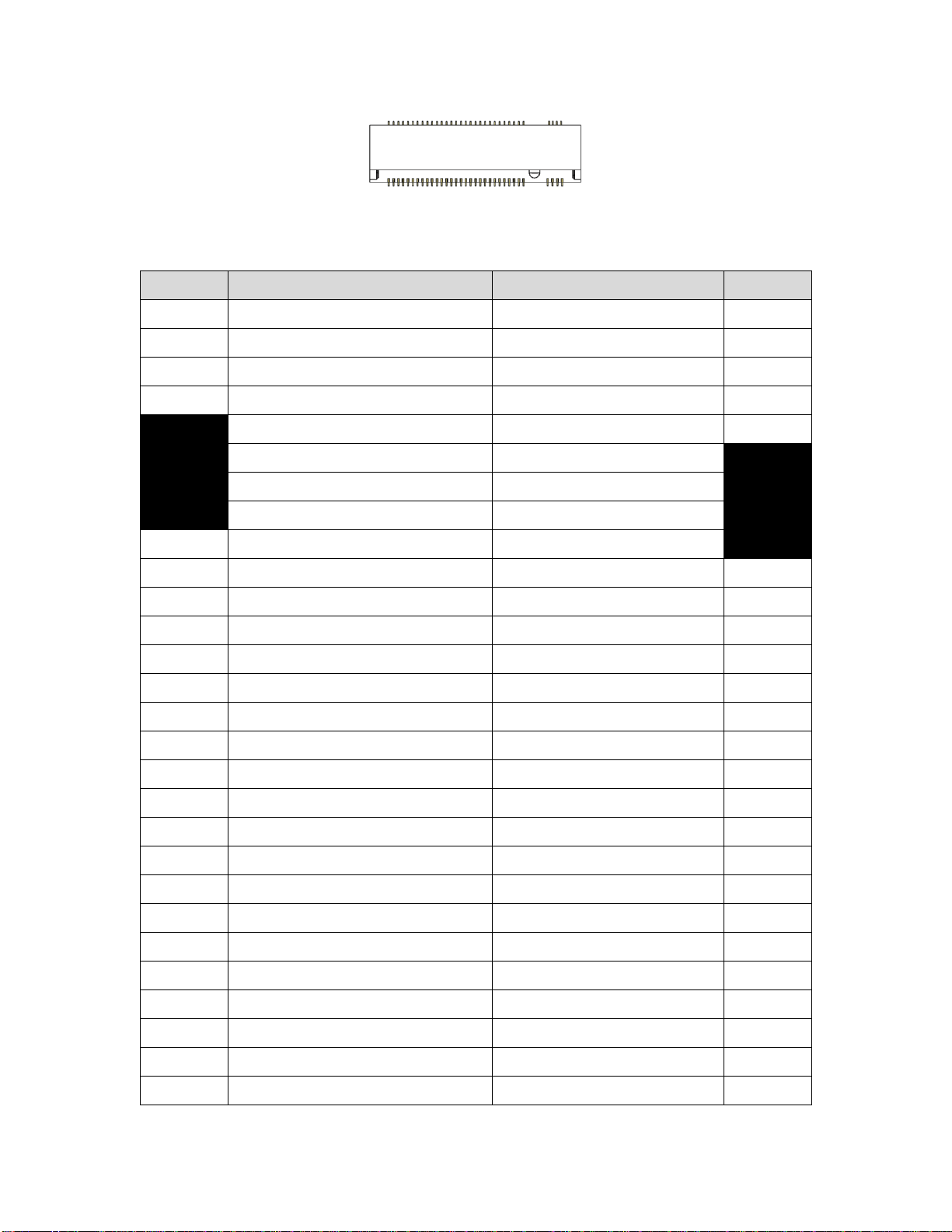
Figure 1
shows the approximate location of the
major components
on
the top
side
of SOtM sMB-Q370.
Figure 1 : Motherboard layout
USB2.0X2
DP + HDMI
USB3.0X4 LAN
B
C
D
E
A
G
H
I
J K L M N O P
Q
R
S
T
U
V
W
X
Y
Z
AA
AB
F

4
TABLE 2. SOtM sMB-Q370 COMPONENTS (SHOWN IN FIGURE 1)
5
The board supports 9th & 8th generation Intel Core processors. Other processors may
be supported in the future. This board supports processors with a maximum wattage
of 95W (8 core 35W & 6 core 95W) Thermal Design Power (TDP).
NOTE
This board has specific requirements for providing power to the processor.
Additional power required will depend on configurations chosen by the integrator.
NOTE
To be fully compliant with all applicable DDR SDRAM memory specifications, the
board should be populated with DIMMs that support the Serial Presence Detect
(SPD) data structure. This allows the BIOS to read the SPD data and program the
chipset to accurately configure memory settings for optimum performance. If non-
SPD memory is installed, the BIOS will attempt to correctly configure the memory
settings, but performance and reliability may be impacted or the DIMMs may not
function under the determined frequency.
The Motherboard has wo288-pin DDR4 U-DIMM sockets with gold-plated contacts.

6
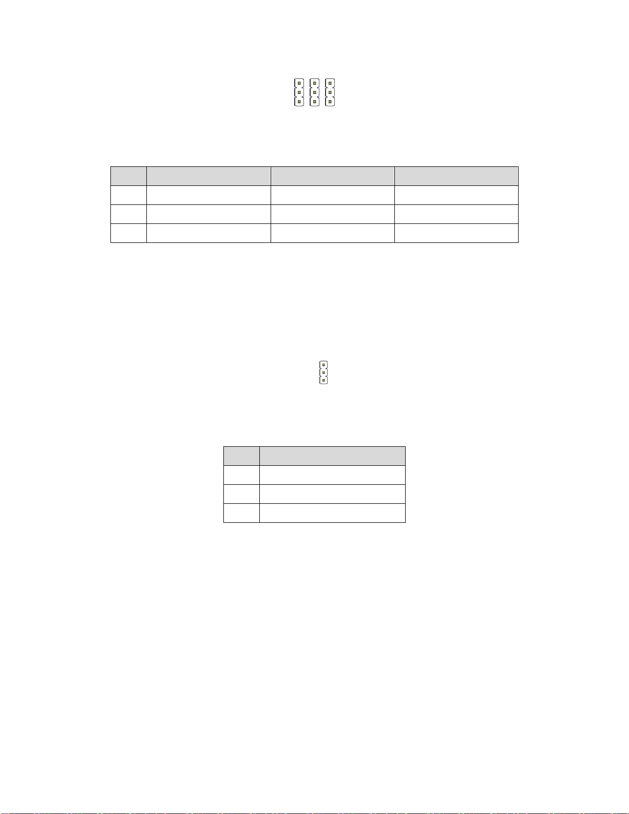
Figure : Front Panel Connector(J_FIO_1)
PIN
NAME
Description
PIN
NAME
Description
1
HDD_POWER_LED
(Orange color)
Pull-up resistor
(330Ω) to +5V
2
POWER_LED_MAIN
(Green color)
[Out] Front panel
LED (Green)
3
HDD_LED#
(Orange color)
[Out] Hard disk
activity LED
4
POWER_LED_ALT
(Green color)
[Out] Front panel
LED (Yellow)
5
GROUND
(Blue color)
Ground
6
POWER_SWITCH#
(Red color)
Power button
7
RESET_SWITCH#
(Blue color)
Reset switch
8
GROUND
(Red color)
Ground
9
+5V_DC
(Black color)
Power
10
KEY
(Black color)
No pin
Table : Front Panel Connector
Figure : USB3.0 header(FP_USB3_1, Blue color)
PIN
NAME
NAME
PIN
1
5V_USB31
NA
2
PCH_USB31RX_5N
5V_USB32
19

7
3
PCH_USB31RX_5P
PCH_USB31RX_6N
18
4
GND
PCH_USB31RX_6P
17
5
PCH_USB31TX_5N
GND
16
6
PCH_USB31TX_5P
PCH_USB31TX_6N
15
7
GND
PCH_USB31TX_6P
14
8
USB_PCH_DN6
GND
13
9
USB_PCH_DP6
USB_PCH_DN2
12
10
NC
USB_PCH_DP2
11
Table : 20-pin USB3.0 header pin-out reference
Figure : LVDS Connector(J5, Ivory color)
PIN
NAME
NAME
PIN
1
VCC3
BKLT_PWR
2
3
VCC3
BKLT_PWR
4
5
LVDS_DDC_SCL
LVDS_DDC_SDA
6
7
GND
LVDS_HPDET
8
9
LVDS0_LINK1_CON_DP
LVDS0_LINK0_CON_DP
10
11
LVDS0_LINK1_CON_DN
LVDS0_LINK0_CON_DN
12
13
GND
GND
14
15
LVDS0_LINK3_CON_DP
LVDS0_LINK2_CON_DP
16
17
LVDS0_LINK3_CON_DN
LVDS0_LINK2_CON_DN
18
19
GND
GND
20
21
LVDS1_LINK1_CON_DP
LVDS1_LINK0_CON_DP
22
23
LVDS1_LINK1_CON_DN
LVDS1_LINK0_CON_DN
24
25
GND
GND
26
27
LVDS1_LINK3_CON_DP
LVDS1_LINK2_CON_DP
28
29
LVDS1_LINK3_CON_DN
LVDS1_LINK2_CON_DN
30
31
GND
GND
32
8
33
LVDS1_CLK_CON_DP
LVDS0_CLK_CON_DP
34
35
LVDS1_CLK_CON_DN
LVDS0_CLK_CON_DN
36
37
GND
GND
38
39
BKLT_PWR
BKLT_PWR
40
Table : 40-pin LVDS data header pin-out reference
Figure: LPC header pin-out(LPC_HDR1, Black color)
PIN
NAME
NAME
PIN
1
LPC_LAD0
VCC3
2
3
LPC_LAD1
PLTRST_BUFFER_N
4
5
LPC_LAD2
L_FRAME_N
6
7
LPC_LAD3
GND
8
9
PORT80_CLK
Table : LPC header pin-out
Figure : LVDS inverter power header pin-out(JBKL1, Red color)
PIN
NAME
Description
1
LVDS_BKTEN_R
Backlight enable
2
LVDS_PWM
Backlight PWM control
3
12V/19V
Inverter power
4
12V/19V
Inverter power
9
5
GND
Ground
6
GND
Ground
7
BRIGHT_UP-
BRIGHTNESS UP
8
BRIGHT_DOWN-
BRIGHTNESS DOWN
Table : 8-pin LVDS inverter power header signals
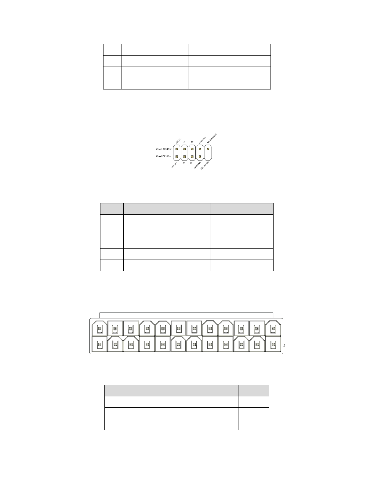
Figure : Dual USB2.0 pin-out(FP_USB2_1, FP_USB2_2, Black color)
PIN
NAME
PIN
NAME
1
5V_USB
2
5V_USB
3
Data (negative)
4
Data (negative)
5
Data (positive)
6
Data (positive)
7
Ground
8
Ground
9
Key (no pin)
10
No Connect
Table : Dual USB 2.0 Header
Figure : ATX 24pin pin-out(ATX24P_1, Ivory color)
PIN
NAME
NAME
PIN
1
3.3V
3.3V
13
2
3.3V
-12V
14
3
COM
COM
15

10
4
5V
PS-ON
16
5
COM
COM
17
6
5V
COM
18
7
COM
COM
19
8
PW-OK
-5V
20
9
5VSB
5V
21
10
12V
5V
22
11
12V
VCC
23
12
3.3V
COM
24
Table : ATX 24pin signals
Figure: ATX 8pin pin-out(ATX8P_1, Ivory color)
PIN
NAME
NAME
PIN
1
GND
12V
5
2
GND
12V
6
3
GND
12V
7
4
GND
12V
8
Table: ATX 8pin signals
Figure : AT/ATX Header(JPSON1, Black color)
PIN
NAME
1
PSON_AT_N
2
SW_PWRBT_N
3
NC
Jumper (1-2) : AT mode
Jumper (2-3) : NON-AT mode
Table: AT/ATX Header

11
Figure : BKL PWM Header pin-out(BKLPWM1, Black color)
PIN
NAME
1
PCH_BACKLIGHT_PWM
2
BKLT_PWM
3
AD5258BRMZ10_PWM
Jumper (1-2) : BACKLIGHT PWM is from PCH (Default)
Jumper (2-3) : BACKLIGHT PWM is from AD5258BRMZ10
Table : BKL PWM Header
Figure : BKL on/off Header(BL_ON_OFF1, Black color)
PIN
NAME
1
VCC
2
BKLT_EN
3
NC
Jumper (1-2) : On for BKL (Default)
Jumper (2-3) : Off for BKL
Table : BKL on/off Header

12
Figure: BKL Voltage Header(BKLVOL1, Black color)
PIN
NAME
1
VCC
2
PWM
3
VCC3
Jumper (1-2) : VCC (Default)
Jumper (3-3) : VCC3
Table : BKL Voltage Header
Figure : TPM Header(J46, Black color)
PIN
NAME
NAME
PIN
1
3.3V
L_FRAME_N
2
3
LPC_LAD0
NA
5
LPC_LAD1
TPM_PLTRST_N
6
7
LPC_LAD2
GND
8
9
LPC_LAD3
TPMPCLK
10
11
TPM_SERIRQ
GND
12
13
TPM_MOD_N
3.3V
14
15
GND
RST_ESPI_RESET_N
16
Table : TPM Header

13
Figure: fan header pin-out(J_CPU_FAN1, J_FIO_FAN1, White color)
PIN
NAME
1
Ground
2
+12V
3
FAN_TACH
4
FAN_CTRL
Table : Fan Header signals
Figure: CMOS Clear Header(CLCMOS1, )
PIN
NAME
1-2
Clear CMOS
2-3
Normal
Table : CMOS Clear behavior
Note : If you use an external clock like sCLK-EX, it will take around 10 mins to clear CMOS.
So you have to wait more than 10 mins with AC power off.
And sMB-Q370 will reboot a few times automatically after CMOS clears or CMOS values changes.
14
Figure : M.2 M key slot For Storage pin-out(M2M_1, M2M_2, Black color)
PIN
NAME
NAME
PIN
74
3.3Vaux
GND
75
72
3.3Vaux
GND
73
70
3.3Vaux
GND
71
68
SUSCLK(32kHz)(O)(0/3.3V)
PEDET(OC-PCIe/GND-SATA)
69
66
Connector Key
N/C
67
64
Connector Key
Connector Key
65
62
Connector Key
Connector Key
63
60
Connector Key
Connector Key
61
58
N/C
Connector Key
59
56
N/C
GND
57
54
PEWake#(IO)(0/3.3V)
REFCLKP
55
52
PERST#(O)(0/3.3V) or N/C
REFCLKN
53
50
PERST#(O)(0/3.3V) or N/C
GND
51
48
N/C
PETp0/SATA-A+
49
46
N/C
PETn0/SATA-A-
47
44
N/C
GND
45
42
N/C
PERp0/SATA-B-
43
40
N/C
PERn0/SATA-B+
41
38
DEVSLP(O){0/3.3V}
GND
39
36
N/C
PETp1
37
34
N/C
PETn1
35
32
N/C
GND
33
30
N/C
PERp1
31
28
N/C
PERn1
29
26
N/C
GND
27
24
N/C
N/C
25
22
N/C
N/C
23
20
N/C
GND
21

15
18
3.3Vaux
N/C
19
16
3.3Vaux
N/C
17
14
3.3Vaux
GND
15
12
3.3Vaux
N/C
13
10
DAS/DSS#(I){OD}
N/C
11
8
GND
9
6
N/C
N/C
7
4
3.3Vaux
N/C
5
2
3.3Vaux
GND
3
GND
1
Table : M.2 M key slot For Storage signals
Figure : M.2 E key slot For wireless pin-out(M2E_1, M2E_2, Black color)
PIN
NAME
NAME
PIN
74
3.3V
GND
75
72
3.3V
RESERVED/REFCLKn1
73
70
UIM_POWER_SRC/GPIO1/PEWAKE1
#
RESERVED/REFCLKp1
71
68
UIM_POWER_SNK/CLKREQ1#
GND
69
66
UIM_SWP/PERST1#
RESERVED/PETn1
67
64
RESERVED
RESERVED/PETp1
65
62
ALERT# (O)(0/3.3V)
GND
63
60
I2C_CLK (I)(0/3.3V)
RESERVED/PERn1
61
58
I2C_DATA (I/O)(0/3.3V)
RESERVED/PERp1
59
56
W_DISABLE1# (I)(0/3.3V)
GND
57
54
W_DISABLE2# (I)(0/3.3V)
PEWAKE0# (I/O)(0/3.3V)
55
52
PERST0# (I)(0/3.3V)
CLKREQ0# (I/O)(0/3.3V)
53
50
SUSCLK(32kHz) (I)(0/3.3V)
GND
51
48
COEX1(I/O)(0/1.8V)
REFCLKn0
49
16
46
COEX2(I/O)(0/1.8V)
REFCLKp0
47
44
COEX3(I/O)(0/1.8V)
GND
45
42
VENDOR DEFINED
PETn0
43
40
VENDOR DEFINED
PETp0
41
38
VENDOR DEFINED
GND
39
36
UART CTS (I)(0/1.8V)
PERn0
37
34
UART RTS (O)(0/1.8V)
PERp0
35
32
UART RXD (I)(0/1.8V)
GND
33
Connector Key
Connector Key
Connector Key
Connector Key
Connector Key
Connector Key
Connector Key
Connector Key
22
UART TXD (O)(0/1.8V)
SDIO RESET# (I)(0/1.8V)
23
20
UART WAKE# (O)(0/3.3V)
SDIO WAKE# (O)(0/1.8V)
21
18
GND
SDIO DATA3(I/O)(0/1.8V)
19
16
LED2# (O)(OD)
SDIO DATA2(I/O)(0/1.8V)
17
14
PCM_IN/I2S SD_IN (I)(0/1.8V)
SDIO DATA1(I/O)(0/1.8V)
15
12
PCM_OUT/I2S SD_OUT (O)(0/1.8V)
SDIO DATA0(I/O)(0/1.8V)
13
10
PCM_SYNC/I2S WS (I/O)(0/1.8V)
SDIO CMD(I/O)(0/1.8V)
11
8
PCM_CLK/I2S SCK (I/O)(0/1.8V)
SDIO CLK(I)(0/1.8V)
9
6
LED1# (O)(OD)
GND
7
4
3.3V
USB D-
5
2
3.3V
USB D+
3
GND
1
Table : M.2 E key slot For wireless signals
17
Figure : SATA Header pin-out(SATA1, SATA2, SATA3, SATA4, SATA5, SATA6, Black color)
PIN
NAME
1
GND
2
SATA_TX2_C_DP
3
SATA_TX2_C_DN
4
GND
5
SATA_RX2_C_DN
6
SATA_RX2_C_DP
7
GND
Table : SATA Header signals
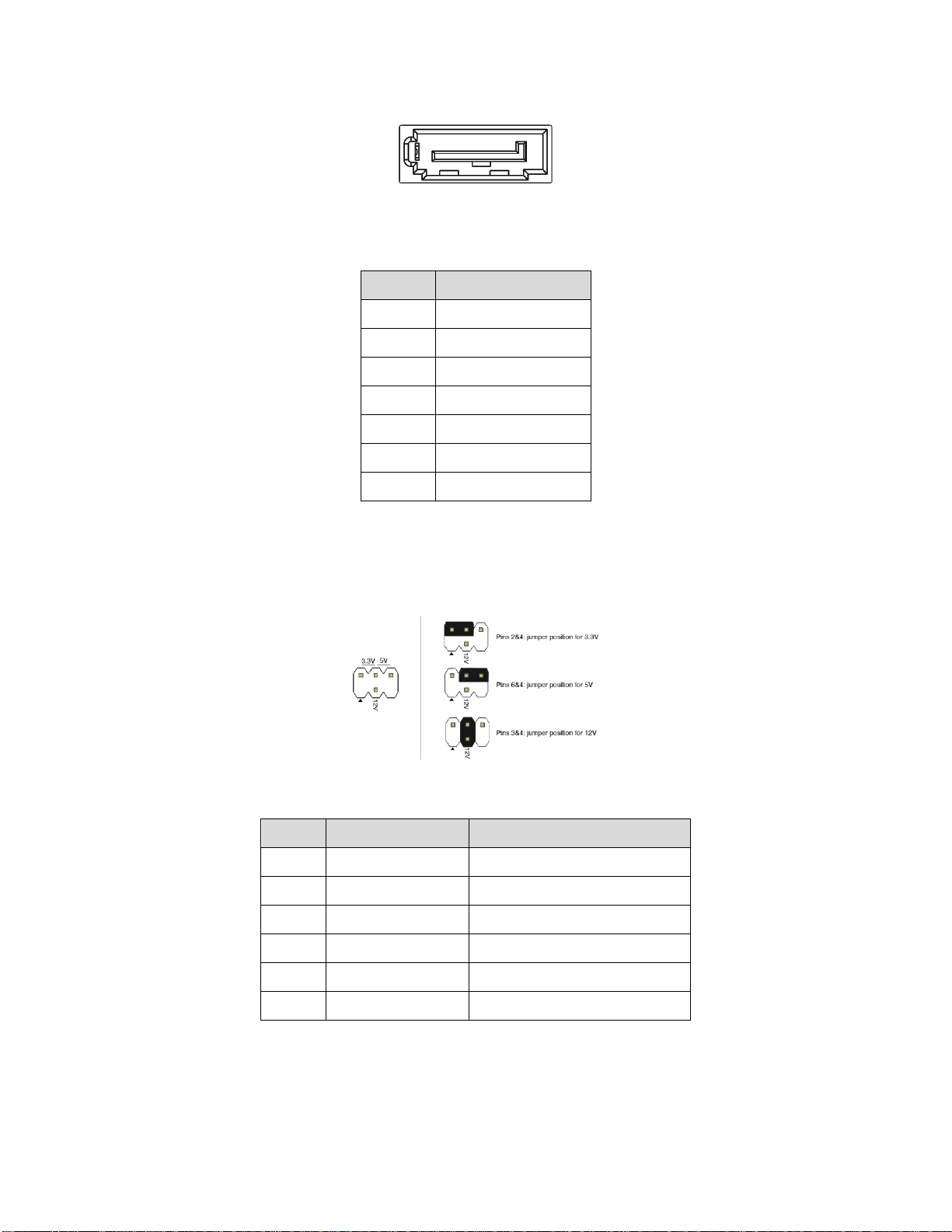
Figure : Panel power Header pin-out(J20, Black color)
PIN
NAME
Description
1
Key
No pin
2
3.3V
3.3V option (default)
3
12V
12V option
4
LCD_VCC
Send voltage to connector
5
Key
No pin
6
5V
5V option
Table : Panel power Header signal
18
Figure : LAN LED On/Off Header(J53, J54, J55, Black color)
PIN
J53
J54
J55
1
LINK_ACTIVITY
LAN1_SPEED_100_R
LAN1_SPEED_1000_R
2
LAN1_LINK_ACTIVITY_L
LAN1_SPEED_100
LAN1_SPEED_1000
3
NC
NC
NC
Jumper (1-2) : LED on
Jumper (2-3) : LED off
Table : LAN LED On/Off
Figure : Boot Delay Time Selection Header(PLTRST_DLY, Black color)
PIN
NAME
1
VR_READY
2
Delay capacitor
3
NC
Jumper (1-2) : Add 2.5 seconds delay time.
Jumper (2-3) : No additional delay time
Table : Boot Delay Time Select
Table of contents
Other SOtM Motherboard manuals


