1 Overview
The STDES-WLC38WA is optimized for performance. The board and IC feature:
• High efficiency (98% typical) synchronous rectifier operating up to 800 kHz
• Low drop-out linear regulator with output current limit and input voltage control loop
• Adaptive rectifier configuration (ARC) mode for enhanced spatial freedom
• 4 V to 12 V programmable output voltage
• 32-bit, 64 MHz Arm® Cortex® M0+ core with 32kB RRAM, 16 KB SRAM, 64kB ROM
• 10-bit A/D converter
• Configurable GPIOs
• I²C slave interface
• Multilevel ASK modulator, enhanced FSK demodulator
• Output overvoltage clamping protection
• Accurate voltage/current measurement for foreign object detection (FOD)
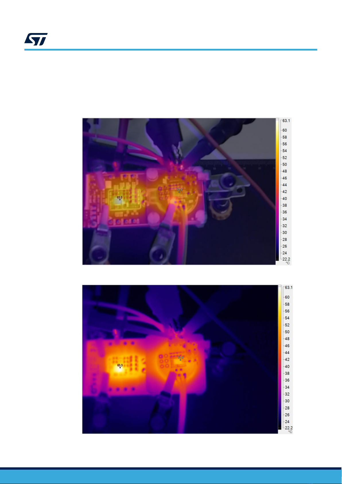
• On-chip thermal management and protections
• Flip chip 40 bumps (2.12 mm x 3.32 mm) package
• Small, ready to use 20 mm board
• I²C connector, GPIO, and INT connector, SOVP resistor
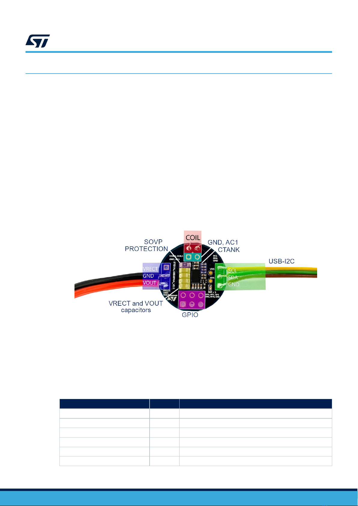
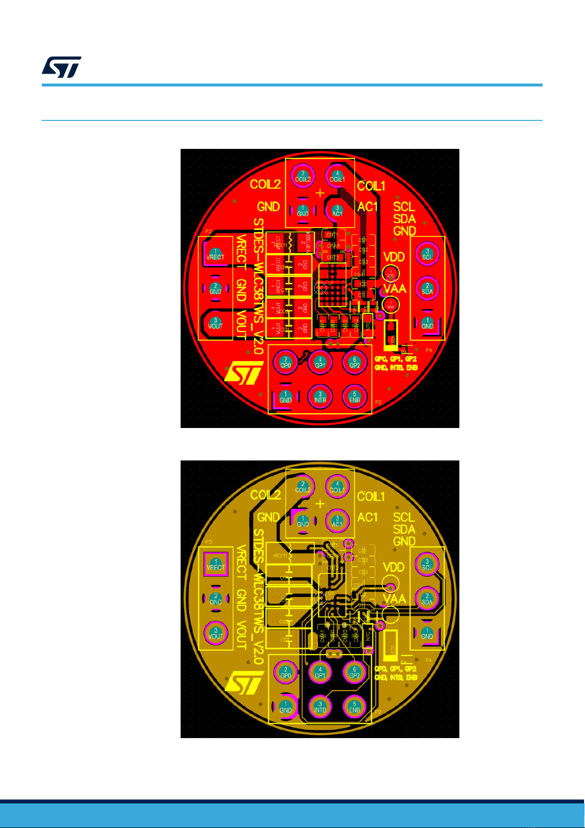
Figure 4. STDES-WLC38WA connection overview
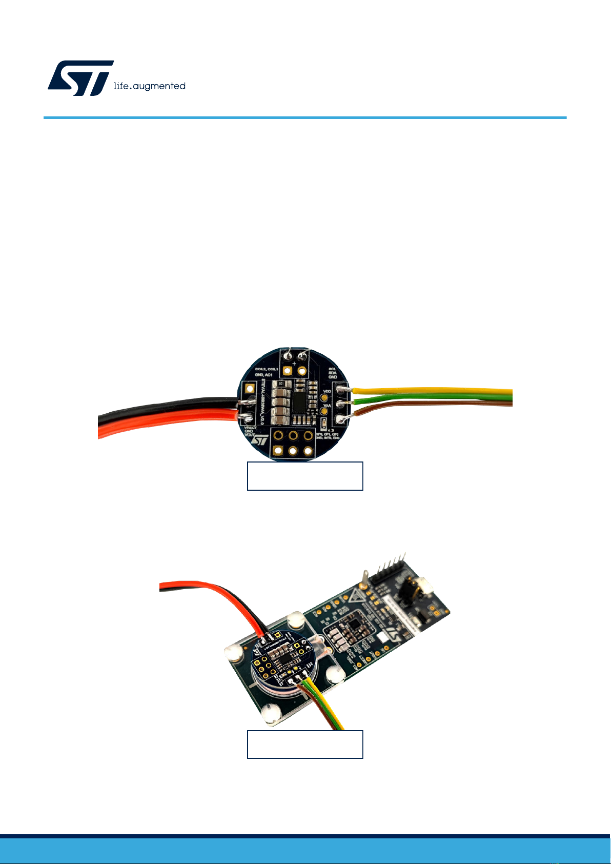
The STDES-WLC38WA is equipped with all components necessary for a standalone operation. The coil has to be
connected to pads (COIL1 and COIL2). The pad labeled as AC1 is used for debug purposes.
The rectifier output is labeled VRECT. The output voltage is VOUT. The I²C interface is used to monitor/control the
device. GPIOs are accessible on the six-pin header.
1.1 Test points
STDES-WLC38WA features several connectors and test points to provide easy access to key signals.
Table 1. Connectors and test points
Connector/test point Name Description
Connector P1 Coil connection and AC1 debug output
Connector P2 GPIO and INT connector
Connector P3 VRECT and VOUT connector
Connector P4 I²C connector
Test point VAA Test point of internal LDO
Test point VDD Test point of internal LDO
TN1440
Overview
TN1440 - Rev 2 page 3/19