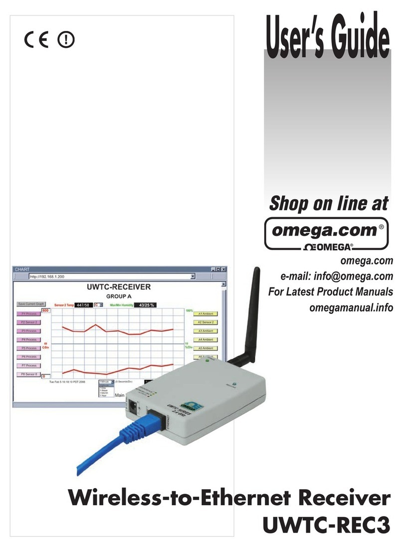
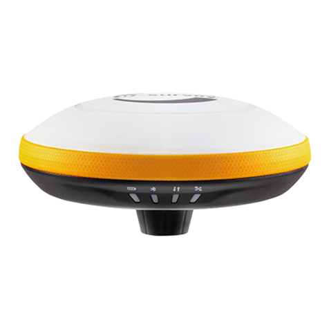
ST STEVAL-WLC38RX User manual

Introduction
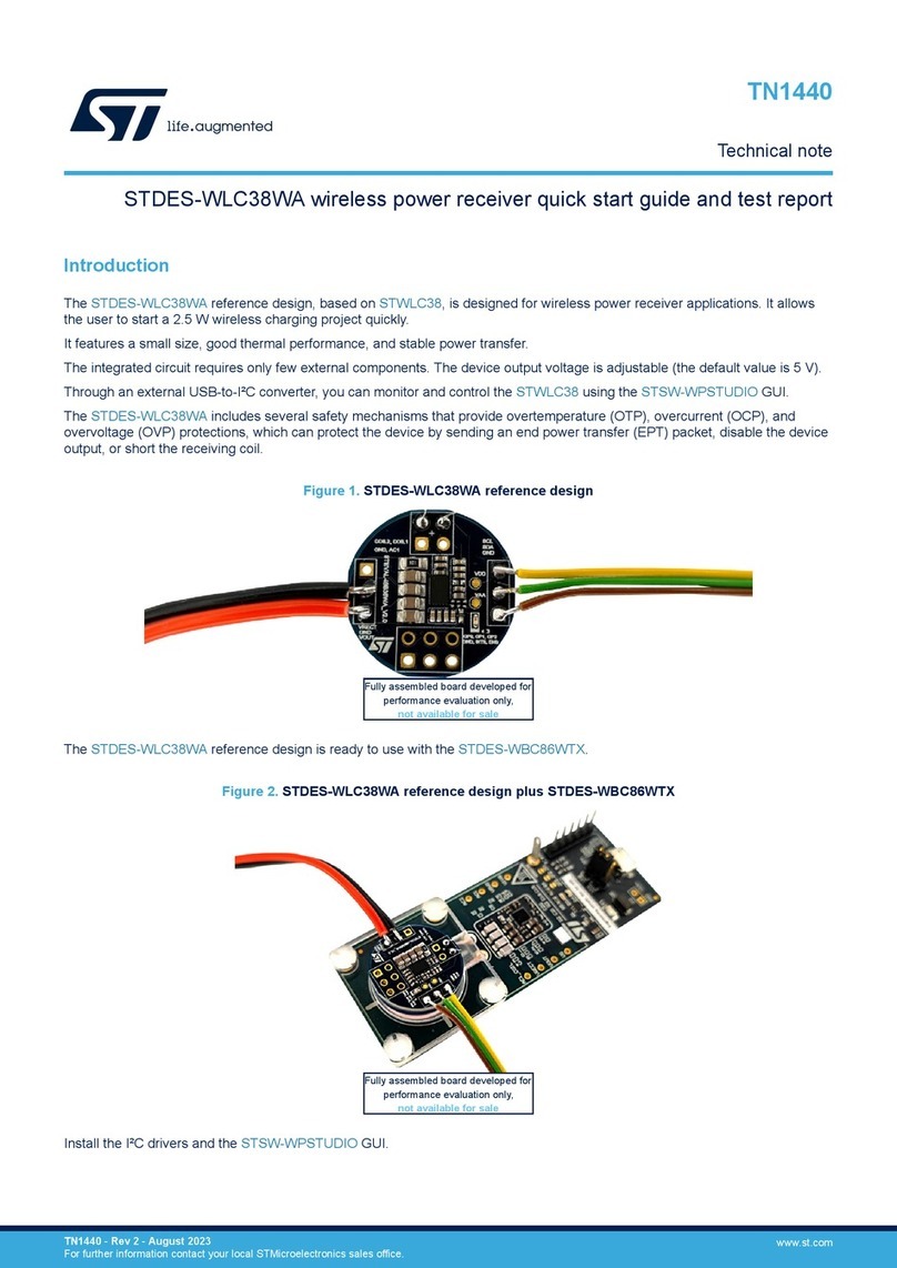
The STEVAL-WLC38RX evaluation board is based on STWLC38 and is designed for wireless power receiver applications. It
allows users to quickly start their 5W Qi-BPP and 15W Qi-EPP compatible wireless charging receiver projects.
The STWLC38 wireless power receiver can manage up to 15 W of power according to the Wireless Power Consortium’s
Extended Power Profile (EPP).
The integrated circuit requires only a few external components and offers high design flexibility. Using an on-board USB-to-I2C
bridge, the user can monitor and control the STWLC38 using the STSW-WPSTUDIO graphical user interface (GUI).
STEVAL-WLC38RX includes several safety mechanisms providing overtemperature (OVTP), overcurrent (OCP) and
overvoltage (OVP) protections as well as foreign object detection (FOD) for reliable designs.
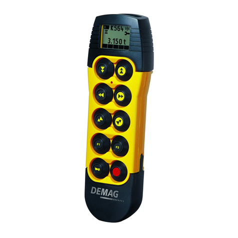
Figure 1. STEVAL-WLC38RX evaluation board
Getting started with the STEVAL-WLC38RX wireless power receiver evaluation
board for 5 W Qi BPP and 15 W Qi EPP applications
UM3154
User manual
UM3154 - Rev 2 - September 2023
For further information contact your local STMicroelectronics sales office. www.st.com

1 Get started
To get started with STEVAL-WLC38RX, you will need the following items to use the reference design kit:
• Evaluation kit components:
–STEVAL-WLC38RX board
• Additional hardware
–STEVAL-WBC86TX for the best results for a 5 W turnkey wireless charging system or any other Qi
BPP or Qi EPP compliant transmitter available on the market
– Electronic load
– Windows PC for measurements and configurations
• Software:
–STSW-WPSTUDIO Wireless Power Studio PC GUI installation package
– I²C drivers
• Application notes:
– Coil selection guide: AN5961
– GUI guide: UM3164
UM3154
Get started
UM3154 - Rev 2 page 2/81

2 Reference design specifications
Target specifications of STEVAL-WLC38RX evaluation board are as follows:
Table 1. reference design specifications
Parameter Description
Qi compatibility Qi 1.3 BPP and EPP protocol
Rx application PCB area 24 mm x 34 mm
Rx coil specifications Inductance 8 uH, DCR 190 mΩ, ACR 225 mΩ
Dimensions 57 mm x 57 mm x 0.42 mm (LD81FP008-1H)
Output voltage (Vout, continuous
operation) 5 V Baseline Power Profile / 9 V Extended Power Profile
Output current (Iout, Load) Recommended current load range is 0.1 – 1 A
Host MCU STM32 used as a reference, the reference I2C driver can be ported to any other
MCU family
USB-to-I2C converter Embedded in the evaluation board
Efficiency 77.6% (5 W operation) with STEVAL-WBC86TX
81% (peak efficiency) with STEVAL-WBC86TX at 3 W
Applicable charging gap between Tx
and Rx coils(z-distance)
3 – 13 mm (5 W output) with STEVAL-WBC86TX transmitter,
maximum 16 mm – stable communication without output enabled
Misalignment between Tx and Rx coils
(x-y offset from the center) 12 mm for 5 W output, 18 mm for stable communication without output enabled
UM3154
Reference design specifications
UM3154 - Rev 2 page 3/81

3 Overview of the Board
The STEVAL-WLC38RX evaluation board is optimized for performance. The board features:
• STWLC38 wireless power receiver chip with BPP and EPP compliant firmware
• Very few external components, optimized BOM and PCB space
• On-chip high efficiency rectifier
• Support for external NTC for thermal monitoring
• On-chip thermal management and protections
• WPC Qi extended power profile (EPP, 15 W) compatible receiver chip
•On board USB-to-I2C converter
• USB Type-C® connector for PC GUI connection
Figure 2. Main board elements
• Series resonant capacitors and the receiving coil together form a resonant circuit. This circuit is in charge
of receiving the power signal, so any components/tracks involved should be rated accordingly
• USB/I2C converter–provides a communication channel between a PC and STWLC38. LED D8 (Red)
indicates that the I2C converter is powered, D9 (yellow) indicates that STWLC38 is connected to the GUI.
LED D10 (Green) indicates that I2C communication was initialized and is ready. Switch S1 resets the
converter. Note that header P3 connects the converter’s I2C signals to the STWLC38 I2C signals. Short the
corresponding pins with a jumper to establish a connection between the two ICs.
• Red LED (D7)–indicates STWLC38 core power status (LED is on when the core is powered).
UM3154
Overview of the Board
UM3154 - Rev 2 page 4/81

3.1 Test points
STEVAL-WLC38RX features several headers and test points to provide easy access to key signals.
Figure 3. Headers and test points
Table 2. header and test point descriptions
Connector Name Description
P1 Rx Coil 4-pin Header: for mounting External RX Coil:
Pin 1,2 AC2; Pin3,4 AC1_COIL
P3 I2C2x4 pin Header: AGND, SDA, SCL, INTB
P6 Control signals 8 pin Header: Programmable GPIOs, ENB, INTB, NTC
P4 VRECT 2-pin Header: VRECT output
P5 VOUT 4-pin Header: VOUT output
P7, P8, P14 GROUND 2-pin Header: Ground connection
P9, P10 GROUND 4-pin Header: Ground connection
P11 VBUS-VOUT 2 Pin Header: VBUS to VOUT Wire Jumper
UM3154
Test points
UM3154 - Rev 2 page 5/81

Connector Name Description
J1 USB-C USB-C Connector
3.2 Basic operating modes
The receiver generally works in two modes - DC (also called Standalone) mode and AC mode.
DC mode is characterized by the wireless receiver being powered from a DC power supply such as external
power supply or USB. This mode is used for Patch and Configuration loading (described later ). Before entering
this mode, device shall not be powered from power transmitter (device is put away from power transmitter or
power transmitter is being powered off).
AC mode is used when the wireless receiver is powered from a wireless power transmitter. A stable and ongoing
power transfer between the transmitter and the receiver is indicated by LED (D7). Make sure that Rx is not
powered by external DC power before entering this mode.
3.3 Functional check
Figure 4. Transmitter and receiver boards setup
The first sign of an ongoing power transfer is the D7 LED, as this LED indicates the internal power supply of the
device is ready. A continuously shining LED indicates a stable power supply, while a blinking or inactive LED
indicates an unstable and/or insufficient power supply.
The LED D7 is permanently OFF means there is no power transfer between the transmitter and the receiver.
Check if the power supply of the transmitter is connected and working properly. Power transfer termination may
also be caused by a large enough misalignment (from an ideal center-to-center position) between receiver and
transmitter coils. This issue is, to a certain degree, mitigated by an [ARC mode] feature, which improves spatial
freedom of the charging.
The LED D7 is blinking means some power is transferred, but the amount is insufficient, or the transfer is
unstable. One of the reasons for such instability may be communication issue between the power transmitter and
the power receiver. The instability may as well be caused by one of the protections (OVTP, OCP, OTP) being
triggered.
The built-in USB-I2C converter features three LEDs. LED D8 (RED) indicates presence of power from the USB
connector (J1). LED D9 (YELLOW) indicates that STWLC38 is connected to the GUI. LED D10 (GREEN)
indicates that I2C communication was initialized and is ready.
UM3154
Basic operating modes
UM3154 - Rev 2 page 6/81

4 Graphical user interface (GUI)
STWLC38 (and other ST wireless charging devices) can be configured using the STCHARGE Wireless Power
Studio GUI (STSW-WPSSTUDIO). The GUI can also be used to control, monitor and program the device.
For more information, please see STCHARGE Wireless Power Studio User Manual.
4.1 Connecting STWLC38 to PC GUI
Step 1. Connect the board to a PC by plugging a USB-C cable into the connector J1.
Make sure the STWLC38 I²C pins are connected to the USB-C connector. This can be done by
shorting the appropriate signals (SDA, SCL, INT) on header P3.
Step 2. Power on the STWLC38 before connecting to the GUI, this can be done in one of the following ways:
Step 2a. Place it onto a power transmitter. The device operates in Rx mode.
Step 2b. Switch it into DC mode by connecting a DC power supply to the STWLC38 VOUT pin. The
voltage must be no higher than 3 V.
Step 2c. Switch it into DC mode by connecting the STWLC38 vout signal to the VBUS pin of the
converter board.
Note: Please note that the Rx registers will be available only if the device is operating in Rx mode, DC
mode is mainly used for updating patch and configuration file.
Step 3. Power up the board and open the GUI on your PC. Click the [Connection] button in the top menu.
Up to two devices can be connected at a time. This allows the user to control both Rx and Tx at the
same time).
Figure 5. PC GUI main screen
UM3154
Graphical user interface (GUI)
UM3154 - Rev 2 page 7/81

Step 4. Select [WLC38] as the Rx and click the [Connect] button on the right side of the window.
Figure 6. Device selection and connection
4.2 Patch and configuration files
Firmware of the device can be updated using a Patch file (a binary file in .memh format). The latest version of the
Patch can be found at STWLC38. Updating the firmware is not required but may improve the performance of the
board.
The device can be configured using a Configuration file, a binary file containing settings of all registers which can
be found in the GUI. The GUI can also be used to generate a custom Configuration file, making it easier to quickly
change configuration of the board and/or transfer the configuration to another board.
In GUI, registers are divided into two groups. The value changes of registers colored in RED will take effect only if
a configuration file is generated and written to the device. Changes of registers colored in BLACK will take effect
immediately and can be saved to the configuration file. During power-up, the values of those registers are set to
the values defined in the configuration file written on the device. Registers that cannot be saved to the
configuration file and whose value is lost upon reboot have this fact noted in the description.
4.3 Configuration file generation
Using the STSW-WPSTUDIO makes generating the Configuration file quite simple.
Step 1. To make sure that the latest values are shown in the GUI, it is recommended to use the [Read
[Rx]WLC38] button to dump values from the device to the GUI. Then, the required changes of the
register may be made. This should be done, especially when going from DC mode to Rx mode.
Step 2. Click the [Write [RX]WLC38] button to save current configuration to temp memory.
UM3154
Patch and configuration files
UM3154 - Rev 2 page 8/81

Step 3. Click the [Save RX] button in the RX Registers tab or the Common registers tab.
Figure 7. Save RX button
Step 4. Enter a Configuration ID number (used for version control) and press [OK].
Figure 8. Configuration ID field
UM3154
Configuration file generation
UM3154 - Rev 2 page 9/81

Step 5. Choose your location for the save file.
After choosing a location, the configuration will be saved as a .memh file in the selected folder.
Figure 9. Save folder selection
4.4 Header file
The GUI can also be used to generate a Header file, a binary .h file containing both Configuration and Patch files.
The Header file makes programming the device using a host MCU easier, as both Configuration and Patch can be
loaded at once by simply including the Header file in the host code.
4.5 Header file generation
A custom Header file can be generated in the Header Generator tab.
Step 1. Start by selecting [WLC38] in the top menu.
Figure 10. Device selection
UM3154
Header file
UM3154 - Rev 2 page 10/81

Step 2. Continue by selecting the patch and configuration files and press [Generate].
A pop-up window will appear, asking to confirm you have selected the correct Patch version.
Figure 11. Confirmation of patch version
Step 3. Choose a save destination.
After choosing a location, the Header file will be saved as a .h file in the selected folder.
Figure 12. Header file save
UM3154
Header file generation
UM3154 - Rev 2 page 11/81

4.6 Programming the device
To program the device, the device must be switched into a so-called DC mode. Before switching to DC mode, first
make sure power transfer is not active. The simplest way to achieve this is to either remove the receiver from the
transmitter or to power down the transmitter. To enter DC mode, connect a DC power supply to the VOUT pins.
This can be done by shorting the P11 jumper, which connects STWLC38’s VOUT to the USB VBUS. Alternatively,
an external power supply can be used. Voltage of the power supply should be higher than 3 V for this purpose.
The device can be programmed in three ways – by changing the register values directly in the GUI, by using a
Header file, which loads both Configuration and Patch files at once, or by loading the two memh files separately
using the GUI.
Note: The values written into the registers via the GUI directly are only stored temporarily and will be lost upon chip
reset.
Step 1. To load the Header file using the GUI, navigate to the Programming tab in the side menu.
Step 2. Select WLC38 in the top menu and [HEADER] in the toggle selector.
Figure 13. Loading the header file
Step 3. Select the .h file you want to write.
The GUI will automatically identify the Patch and Configuration files included in the Header file.
Step 4. Press the [Write] button to load the Header file into the device.
Step 5. To load the memh files (patch and configuration) using the GUI, navigate to the Programming tab in
the side menu.
Note: STWLC38 has 32 kB of RRAM, which allows for multiple erase/rewrite cycles up to 1000 times.
UM3154
Programming the device
UM3154 - Rev 2 page 12/81

Step 6. Select WLC38 in the top menu and [MEMH] in the toggle selector.
Figure 14. Loading the patch and configuration files
Step 7. Select the patch and configuration files you want to write.
Step 8. Press the [Write] button to load the .memh files into the device.
UM3154
Programming the device
UM3154 - Rev 2 page 13/81

5 Device description and operation
5.1 System block diagram
Figure 15. STWLC38 system block diagram
UM3154
Device description and operation
UM3154 - Rev 2 page 14/81

5.2 Integrated power rectifier
The synchronous rectifier is a key block in charge of converting the AC power signal from the receiving coil into a
DC supply rail for the following linear regulator. The rectifier consists of four N-channel MOSFET transistors
arranged into an H-bridge, conveniently driven by a control block that monitors the voltage at the AC1 and AC2
pins to optimize the commutations and to charge the external bootstrap capacitors for the high-side switches.
Different driving schemes for the rectifier switches are possible. The MCU core dynamically selects the optimal
one to maximize the overall efficiency as a function of the operating point.
When designing the filtering capacitor at the output of the synchronous rectifier, keep in mind that the capacitance
value should be designed large enough to minimize the residual AC voltage ripple and to provide sufficient energy
storage to sustain load transients and prevent the transients from impacting the ASK communication with the
transmitter.
5.3 Internal ADC channels monitor
The GUI allows to monitor in real-time key parameters by reading the internal ADC channels of the STWLC38
and plotting voltages, current, and temperatures. For further details please refer to the GUI user manual UM3164.
Figure 16. PC GUI charts
5.4 Main LDO regulator
The main LDO regulates the rectified voltage to a target value specified by the user. The output voltage is
configurable in 4 V – 12 V range with a 25 mV step. The default value of output voltage is 5 V for BPP (5W) mode
and 9 V for EPP (15W) mode respectively. However, the target value can be easily changed in the GUI or by an
external host controller.
The main LDO regulator is equipped with two protections:
1. IVL (input voltage loop): when the Vrect voltage falls under a set threshold, the Vout is temporarily disabled
until the Vrect rises above the threshold again. The default threshold for this protection is 3 V but can be
adjusted in 3.5 V to 10.5 V range with a 0.5 V step.
2. OCP (overcurrent protection): this protection is triggered when the rectifier current rises above a set
threshold. The threshold can be adjusted to a value between 1.25 A and 1.93 A.
3. RX UVLO (undervoltage protection): when VRECT falls under a set threshold, the set action may be triggered
as send EPT or permanent disable of VOUT.
4. Output short circuit protection is realized by a combination of overcurrent protection (OCP) and undervoltage
protection (RX UVLO) mechanisms.
UM3154
Integrated power rectifier
UM3154 - Rev 2 page 15/81

To maintain rectifier stability and ASK communication reliability , it is recommended to provide a certain minimum
load to the rectifier. STWLC38 is equipped with Iload ballast function which draws sufficient current from the
rectifier when the output load current is too small.
The rectifier current consists of the Iload ballast current, the output load current and the IC consumption current.
The Iload ballast current is automatically adjusted to maintain the minimal total load current of the rectifier, as set
in the RX ILOAD BALLAST register.
Naturally when the sum of the output load current and IC consumption exceeds the RX ILOAD BALLAST
threshold value there is no additional current sinked by ILOAD BALLAST block and it is disabled and will be
automatically re-enabled when the total current would drop below the threshold.
5.5 Chip under voltage lockout
STWLC38 is equipped with an under voltage lockout, which triggers when the VAA voltage drops below 2 V,
which results in the device being powered down. Normal operation is resumed as soon as the VAA voltage rises
above 2.1 V.
5.6 Chip enable
The device can be disabled (forced into reset) by pulling the chip enable signal high. When the chip enable signal
is released and left to be pulled down to ground, the device resumes normal operation. If the STWLC38 is in reset
mode, then AC1 and AC2 are connected to GND to protect the device.
5.7 Power up sequence
When the STWLC38 receiver is placed onto a power transmitter, and the patch and configuration files are loaded
into the device, it will initiate communication with the transmitter. After completing all the necessary steps
described in the Qi specification, power transfer is established.
If Patch and/or Configuration files are not loaded, the device will not initialize the communication, therefore power
transfer will not be established. Please refer to Section 4.6 Programming the device for device programming
instructions. The communication will also not be initialized if either the Patch or Configuration or both files are
corrupted.
During the initial phase of the power transfer STWLC38 operates in ARC mode, ST’s proprietary mode, which
makes the power-up sequence smoother and more reliable. For more information, see Section 5.12 Adaptive
rectifier configuration (ARC) mode .
Once the VRECT voltage rises high enough, the internal power management system starts operating. The digital
core is powered up and ready to control the internal circuitry. Default device settings are used until the digital core
is woken up after which the firmware loads settings saved in the Cofiguration file saved in NVM. The device is
now ready to operate.
5.8 LDOs
The device is equipped with two internal low drop-out regulators (LDOs) – a 2.5 V and a 1.1 V one, with the later
deriving its power from the former.
The 1.1 V LDO powers the digital part of the IC, while the 2.5 V LDO powers the analog part of the IC but can
also be used to power external low-power circuitry (such as LEDs). The maximum current externally drawn from
this LDO shall not exceed 20 mA.
• External LDO capacitors should be placed as close to the IC as possible.
• Connect a 1 μF filtering capacitor between the VDD pin and ground.
• Connect a 4.7 μF filtering capacitor between the VAA pin and ground.
5.9 Protections overview
STEVAL-WLC38RX board uses both hardware and software protections to ensure safe operation of both the
device and the board. The purpose of those protections is to avoid damage caused by unexpected operating
conditions – over-voltage and/or over-current. Temperature is monitored as well – the device is equipped with
both internal temperature sensor and pins for external NTC connection.
The majority of software protections can be configured in a GUI and/or by a host controller.
Each software protection can also be configured to disable the device's output and force the receiver to send an
EPT (end power transfer) packet when triggered. If the transmitter receives this packet, it should terminate power
transfer immediately.
UM3154
Chip under voltage lockout
UM3154 - Rev 2 page 16/81

Overvoltage protections (OVP)
• Ping overvoltage protection (POVP)
– Protects the device against excessive rectifier voltage (VRECT) during the ping phase (first few
milliseconds after the power-up)
– The threshold is set to 14 V and is released as soon as the rectifier voltage drops below 11 V.
– Gets disabled after the digital part of the device is powered up (the internal 2.5 V LDO reaches the
target value).
– When triggered, AC1 and AC2 pins of the device are shorted to ground
– Cannot be disabled, and the threshold cannot be adjusted
• Soft overvoltage protection (SOVP)
– Connects external resistors between the VRECT node and ground. This causes the VRECT voltage
to drop, without dropping low enough to lose communication with the transmitter.
– Can be disabled in the GUI
– Can be configured to disable VOUT when triggered
– Can also be configured to force the receiver to send EPT packet when triggered
• Hard overvoltage protection (HOVP)
– Shorts AC1 and AC2 pins to ground when triggered
– Can be disabled in the GUI
– This protection can be configured to disable VOUT when triggered
– The threshold of this protection can be set from 6 to 18 V with a 2 V step
• Firmware OVP
– This protection can be configured to disable VOUT when triggered
– The protection can also be configured to force the receiver to send EPT packet when triggered
– The threshold of this protection can be set in range of 0 to 18 V
Undervoltage protections (UVLO)
• Input voltage loop (IVL)
– It monitors the VRECT voltage and automatically reduces the device's output to maintain VRECT at
the set threshold.
– The threshold can be set from 3 to 10.5 V with a 0.5 V step. The default value is 4 V.
• RX UVLO
– It monitors VRECT voltage and disables the device’s output when VRECT drops below a set
threshold.
– It can be configured to disable VOUT when VRECT drops below a set threshold.
– Can also be configured to force the receiver to send EPT packet when triggered
– The threshold can be set from 3 to 10.5 V with a 0.5 V step
– Disabled by default
Overcurrent protections (OCP)
• Hardware OCP
– Monitors the output current
– Can be configured to disable VOUT when triggered
– Can also be configured to force the receiver to send EPT packet when triggered
– The threshold can be set to either 1.25, 1.5, 1.75 or 1.93 A
• Firmware OCP
– Monitors the output current
– Can be configured to disable VOUT when triggered
– Can also be configured to force the receiver to send EPT packet when triggered
– The treshold can be set from 0 to 1.93 A with 1 mA step
Overtemperature protections (OVTP)
UM3154
Protections overview
UM3154 - Rev 2 page 17/81

• Hardware thermal shutdown (TSHUT)
– Can be configured to disable VOUT when triggered
– The threshold can be set from 105 to 135 °C with a 10 °C step.
• Firmware OVTP
– Can be configured to disable VOUT when triggered
– Can also be configured to force the receiver to send EPT packet when triggered
– The threshold can be set from 105 to 135 °C with 0.1 °C step.
• NTC OVTP
– Senses NTC voltage, usually used for coil temperature monitoring
– Can be configured to disable VOUT when triggered
– Can also be configured to force the receiver to send EPT packet when triggered
– The threshold can be set from 0 to 2.5 V.
5.9.1 Soft overvoltage protection (SOVP)
SOVP protects the device against excessive rectifier voltage. When VRECT rises above a set threshold, the
device will try to lower its value by connecting external power resistors (connected to IEXT pin) from VRECT to
ground through internal transistors. This approach should achieve lowering the rectifier voltage without losing
communication with the transmitter. Therefore, triggering this protection does not necessarily lead to regulation
failure or power transfer termination. The protection can also be configured to disable the output and/or force the
receiver to send EPT packet when triggered.
The SOVP can be set to either dynamic or static operation. In dynamic mode , when VRECT > VOUT SET +
SOVP threshold, IEXT switch will be turned-on.
In static mode , when VRECT > 12 V + SOVP threshold, IEXT switch will be turned-on.
The SOVP threshold is programmable from 2 V to 5 V in step sizes of 0.2 V. It can be set by STSW-WPSTUDIO
PC GUI tool or host controller via I2C. SOVP is released when VRECT < SOVP threshold - 1 V.
In dynamic mode, the SOVP threshold is output setting dependent:
• Output enabled: the threshold is set as output voltage + margin
• Output disabled: the threshold is set to 12 V + margin
In dynamic mode the user may accidentally trigger protection. As previously mentioned, the threshold is set
relative to the output voltage. When changing the output voltage setting, the SOVP threshold is adjusted
automatically. However, the regulation loop is quite slow and may not be fast enough to accommodate a large
voltage change. This might cause the rectifier voltage to temporarily exceed the SOVP threshold. Therefore, it is
advised to change the output voltage slowly (in multiple smaller steps).
Figure 17. SOVP Rx protection threshold setting
UM3154
Protections overview
UM3154 - Rev 2 page 18/81

Figure 18. SOVP Rx protection settings
5.9.2 Hard overvoltage protection (HOVP)
HOVP is the fastest (hardware) over-voltage protection, which prevents the rectifier voltage from rising above a
safe level. The default threshold value is 18 V. Triggering the protection causes STWLC38 to short AC1 and AC2
to ground, effectively shorting the receiving coil. This protection should be used as the last measure, as shorting
the receiving coil will cause a significant rise in the transmitter current. Therefore, the HOVP threshold should be
set higher than any other STWLC38 over-voltage protection (but still lower than AMR listed in the datasheet).
HOVP release value depends on SOVP setting.
• If SOVP is enabled, HOVP is released at SOVP threshold
• If SOVP is disabled, HOVP is released at 12 V + SOVP margin (refer to SOVP)
Figure 19. HOVP Rx protection threshold setting
UM3154
Protections overview
UM3154 - Rev 2 page 19/81

Figure 20. HOVP Rx protection settings
SOVP enabled, the VRECT voltage oscillates between the HOVP trigger threshold (18 V) and SOVP threshold.
Figure 21. VRECT and OVP thresholds
UM3154
Protections overview
UM3154 - Rev 2 page 20/81
Table of contents
Other ST Receiver manuals