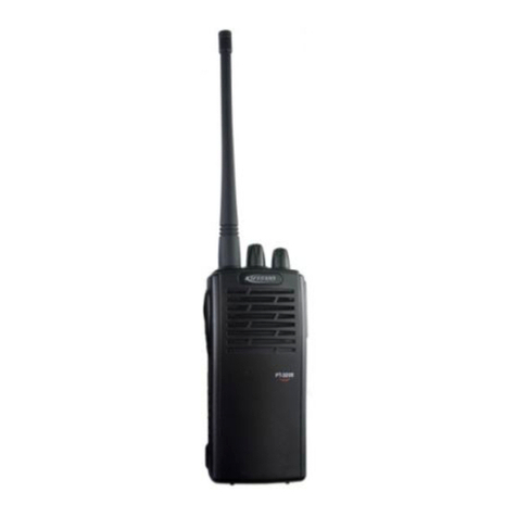
Standart Horizont HX380 User manual

1
SERVICE MANUAL
VHF FM Marine Transceiver
HX380
EM039N90A

2
Specifications
General
Frequency Ranges: 156.025 MHz - 162.000 MHz (Marine Band)
134.000 MHz - 174.000 MHz (LMR Band)
Channel Spacing: 25 kHz / 12.5 kHz
Frequency Stability: ±2.5 ppm (–30 °C to +60 °C)
Emission Type: 16K0G3E (Marine Band)
16K0F3E (LMR Band: Wide)
11K0F3E (LMR Band: Narrow)
Antenna Impedance: 50 Ω
Supply Voltage: 7.4V DC, Negative Ground (Battery Terminal)
Current Consumption: 320 mA (Receive, Typical at AF MAX.)
50 mA (Standby)
1.6 A / 0.8 A (TX: 5 W / 1W)
Operating Temperature: –30 °C to +60 °C
Case Size (W x H x D): 57 x 133 x 33 mm (w/o knob & antenna)
Weight (Approx.): 320 g (w/FNB-V105LI, Belt Clip, & Antenna)
Transmitter
RF Power Output: 5 W / 1 W (@7.4 V )
Modulation Type: Variable Reactance
Maximum Deviation: ±5.0 kHz (Wide) / ±2.5 kHz (Narrow)
Spurious Emission: –36 dBm (<1 GHz), –30 dBm (>1 GHz)
Microphone Impedance:2kΩ
Receiver
Circuit Type: Double-Conversion Superheterodyne
Intermediate Frequencies: 1st: 67.65 MHz, 2nd: 450 kHz
Adjacent Channel Selectivity: 70 dB typical (Wide),
60 dB typical (Narrow)
Intermodulation: 68 dB typical
Sensitivity (LMR Band): –6 dBµV (0.25 µV) for 12 dB SINAD
Selectivity (Wide): 12 kHz / 25 kHz (–6 dB / –60 dB)
Selectivity (Narrow): 6 kHz / 18 kHz (–6 dB / –60 dB)
AF Output (Internal SP): 700 mW @16 W for 10 % THD (@7.4 V)
AF Output (External SP): 350 mW @8 W for 10 % THD (@7.4 V)
Performance specifications are nominal, unless otherwise indicated, and are subject to change without notice.
Measured in accordance with TIA/EIA-603.
Important Note
The HX380 was assembled using Pb (lead) free solder, based on the RoHS specification.
Only lead-free solder (Alloy Composition: Sn-3.0Ag-0.5Cu) should be used for repairs performed on this appara-
tus. The solder stated above utilizes the alloy composition required for compliance with the lead-free specifica-
tion, and any solder with the above alloy composition may be used.

3
Exploded View & Miscellaneous Parts
Unsolder these two battery terminals
to remove the MAIN Unit
from the Rear Panel Assy
Important Note: To ensure the radio is water
proof, make sure the gasket is installed on the
chassis correctly and is not pinched when in-
serted into the front case.
RA1096000
COIL SPRING (085RIGHT)
CS2088101
TERMINALASSY
RA119470A
RUBBER PACKING (TERMINAL)
RA1195000
RUBBER PACKING (CASE)
RA1193700
CASE COVER (REAR)
RA046760A
O RING (ANT)
CP9670001
REAR CASE ASSY
CP9672001
BELT CLIP ASSY
CS2087401
MAIN ASSY
RA107910A
LATCH NAIL
CP9671001
FRONT PANELASSY
(includes Speaker & Window)
RA119510A
LATCH PLATE
RA1194400
HOLDER (PTT)
RA1194300
RUBBER KNOB (PTT)
RA1194000
RUBBER KNOB
RA1193900
VOLUME KNOB
RA1079500
RUBBER PACKING (VOL)
G6090202
LCD
RA125280B
SPONGE RUBBER (WINDOW)
RA107890A
LIGHT GUIDE (LCD)
RA1089600
REFLECTORSHEET
RA1081000
INTERCONNECTOR(LCD)
RA1079400
RING NUT (VOL)
RA1194200
RUBBER CAP (MIC)
RA108700B
KNOB SCREW (SP/MIC)
RA1238000
SHEET (HEAT 6X5 t0.5)
REF.
VXSTD P/N
U02310020
U24108020
U44105001
U9900068
DESCRIPTION
SEMS SCREW SM3X10SUS
BIND HEAD TAPTITE-B M2X8SUS
PAN HEAD TAPTITE-B M2X5
PAN HEAD TAPTITE-B M2X4NI#3
QTY.
1
2
10
3
RA1222500
MIC HOLDER RUBBER (L)
NOTE
The mic element must be des-
oldered and removed from the
PCB on order to reinstall its
protective rubber cover.
Therefore, be careful not to re-
move this cover unless mic el-
ement replacement is neces-
sary.
RA0919700
O RING (6X2.2)
DESCRIPTION
CAT460 Antenna
FNB-V105LI Li-Ion Battery Pack
NC-90B 120VAC Wall Charger (Type-A plug)
NC-90C 230VAC Wall Charger (Type-C plug)
NC-90U 230VAC Wall Charger (Type-BF plug)
CD-48 Charger Cradle
VXSTD P/N
Q3000176
AAG43X001
Q9500142
Q9500143
Q9500144
AAH01X001

4
Note

5
Block Diagram

6
Note

7
1. Circuit Configuration by
Frequency
The receiver is a double-conversion superheterodyne
with a first intermediate frequency (IF) of 67.65 MHz and
a second IF of 450 kHz. Incoming signal from the antenna
is mixed with the local signal from the VCO/PLL to pro-
duce the first IF of 67.65 MHz.
This is then mixed with the 67.2MHz second local oscilla-
tor output to produce the 450 kHz second IF. This is de-
tected to give the demodulated signal.
The transmit signal frequency is generated by the PLL
VCO, and modulated by the signal from the microphone.
It is then amplified and sent to the antenna.
2. Receiver System
2-1. FRONT-END RF AMPLIFIER
Incoming RF signal from the antenna is delivered to the
Main Unit and passes through Low-pass filter, antenna
switching diode D1004 (RLS135), high-pass filter and re-
moved undesired frequencies by varactor diode (tuned
band-pass filter) D1012 and D1013 (both 1SV325).
The radio signal is supplied to the RF amplifier Q1025
(2SC5006) amplified, applied to a tuned band pass filter.
The signal is then applied to the first mixer.
2-2. FIRST MIXER
The 1st mixer consists of the Q1036 (3SK293). Buffered
output from the RX VCO Q1040 (2SK508) is amplified by
Q1038 (2SC5005) to provide a pure first local signal be-
tween 223.675 and 229.650 MHz (Marine Band) or 201.650
and 241.650 MHz (LMR Band) for injection to the first
mixer.
The IF signal then passes through monolithic crystal fil-
ter XF1001 (±7.5 kHz BW) to strip away all but the de-
sired signal.
2-3. IF AMPLIFIER
The first IF signal is amplified by Q1041 (2SC4215Y). The
amplified first IF signal is applied to FM IF subsystem IC
Q1046 (BA4116FV) which contains the second mixer, sec-
ond local oscillator, limiter amplifier, noise amplifier, and
RSSI amplifier.
The signal from reference oscillator X1003 is applied to
FM IF subsystem IC Q1046 (BA4116FV) which increase
the frequency by 4 times, mixes with the First IF signal to
become the Second IF 450kHz.
The second IF then passes through the ceramic filter
CF1001 (LTM450GW for Wide band) or CF1002
(LTM450FW for Narrow band) to strip away unwanted
mixer products, and is applied to the limiter amplifier in
Q1046 (BA4116FV), which removes amplitude variations
in the 450 kHz IF, before detection of the speech by the
ceramic discriminator CD1001 (JTBM450CX24).
2-4. AUDIO AMPLIFIER
Detected signal from Q1046 (BA4116FV) is applied to De-
Emphasis circuit Q1009-3/-4 (LM2902PW). The signal
which appeared from Q1009 (LM2902PW) is fed through
the AF mute switch Q1045 (TC7S66FU) and the buffer
amplifier Q1009-1 (LM2902PW) to the AF volume
(VR1001). The audio signal is applied to audio amplifier
Q1005 (TDA2822L). The output signal from Q1005
(TDA2822L) is in audio speaker.
2-5. SQUELCH CIRCUIT
The squelch circuit is composed of a noise amplifier, band-
pass filter, and noise detector within Q1046 (BA4116FV)
and level shifter Q1032 (M62364FP-CH2). When a carrier
isn’t received, the noise at the output of the detector stage
in Q1046 (BA4116FV) is amplified by the level shifter
Q1032 (M62364FP-CH2). The amplified noise is applied
to the band-pass filter section in Q1046 (BA4116FV), then
detected to DC voltage by the detector stage in Q1046
(BA4116FV). The DC voltage is inputted to 98-pin (NOISE
port) of the CPU Q1035 (R5F2L3ACANFP).
When a carrier is received, the DC voltage at the 98-pin of
the CPU Q1035 (R5F2L3ACANFP) becomes “low” level,
because the noise is compressed.
When the detected voltage at the 98-pin of the CPU Q1035
(R5F2L3ACANFP) is “high” level, the 17-pin (AF MUTE)
of the CPU Q1035 (R5F2L3ACANFP) becomes “low” lev-
el. As a result, turns the AF mute switch Q1045
(TC7S66FU) to “OFF” to disable the audio output.
3. Transmitter System
3-1. MIC AMPLIFIER
The AF signal from internal microphone MC1001 or ex-
ternal microphone connected to J1002 (MIC/SP jack) is
amplified with microphone amplifier Q1017-3
(NJM12902V).
This signal is applied to the high pass filter Q1054-1
(LM2904PW) and buffer amplifier Q1020-4 (LM2902PW).
Afterwards, the AF signal is adjusted by the D/A con-
verter Q1032 (M62364FP-CH1). The adjusted AF signal is
applied to the splatter filter Q1017-4 (NJM12902V), Low-
pass filter Q1017-1/-2 (NJM12902V), and buffer amplifier
Q1020-2 (LM2902PW), the mic audio is applied to the D/A
converter Q1032 (M62364FP-CH4) which adjusts the
audio for Max deviation for normal or narrow band op-
eration. The mic audio is then applied to varactor diode
D1031 (HVC383B) that modulates the VCO transmit sig-
nal.
Circuit Description

8
Circuit Description
3-2. DRIVE AND FINAL AMPLIFIER
The modulated signal from the TX VCO Q1042 (2SC4227)
is buffered by Q1038 (2SC5005). Then the signal is buff-
ered by Q1031 (2SC5227) for the final amplifier driver
Q1026 (RQA0004PXDQS). The low-level transmit signal
is then applied to Q1019 (RQA0011DNS) for final amplifi-
cation up to 5watts output power.
The transmit signal then passes through the antenna
switch D1003 (RLS135), low pass filtered to suppress
away harmonic spurious radiation before delivery to the
antenna.
3-3. AUTOMATIC TRANSMIT POWER CONTROL
The current detector Q1012-2 (LM2904RW) detects the
current of Q1026 (RQA0004PXDQS) and Q1019
(RQA0011DNS), and converts the current difference to
the voltage difference.
The output from the current detector Q1012-2
(LM2904RW) is compared with the reference voltage and
amplified by the power control amplifier Q1012-1
(LM2904RW).
The output from Q1012-1 (LM2904RW) controls the gate
bias of the final amplifier Q1019 (RQA0011DNS) and the
driver Q1026 (RQA0004PXDQS).
The reference voltage changes into two values (Transmit
Power “High” and “Low”) controlled by Q1032
(M62364FP-CH8).
4. PLL Frequency Synthesizer
The frequency synthesizer consists of PLL IC, VCO, TCXO
(X1003), and buffer amplifier.
The output frequency from TCXO is 16.8 MHz and the
tolerance is ±2.5 ppm (in the temperature range –30 to
+60 degrees).
4-1. VCO
While the radio is receiving, the RX VCO Q1040 (2SK508)
generates a programmed frequency between 223.675 and
229.650 MHz (Marine Band) or 201.650 and 241.650 MHz
(LMR Band) as 1st local signal.
While the radio is transmitting, the TX VCO Q1042
(2SC4227) generates a frequency between 156.025 and
162.000 MHz (Marine band) or 134.000 and 174.000 MHz
(LMR Band).
During receive, the signal from VCO is amplified by buff-
er amplifier Q1038 (2SC5005). The output signal Q1038
(2SC5005) applied to (a) pin-8 of the PLL IC Q1048
(MB15E03SL) to keep the radio on frequency (b) the 1st
mixer Q1036 (3SK293) as the 1st local signal through
D1029 (DAN235E).
During transmission, the TX signal from the VCO is ap-
plied to buffer amplifier Q1031 (2SC5227) through D1029
(DAN235E).
4-2. PLL
The PLL IC Q1048 (MB15E03SL) consists of reference di-
vider, main divider, phase detector, charge pumps and
pulse swallow operation. The reference frequency from
TCXO is inputted to 1-pin of PLL IC Q1048 (MB15E03SL)
and is divided by reference divider.
The other hand, inputted feed back signal to pin 8 of PLL
IC Q1048 (MB15E03SL) from VCO is divided with the
dividing ratio which becomes same frequency as the out-
put of reference divider. These two signals are compared
by phase detector, the phase difference pulse is generat-
ed.
The phase difference pulse and the pulse from through
the charge pumps and LPF is converted into DC voltage
to control the VCO.
The oscillation frequency of VCO is locked by the control
of this DC voltage.
The PLL serial data from CPU Q1035 (R5F2L3ACANFP)
is sent with three lines of CLK (81-pin), DATA (82-pin)
and P STB (83-pin).
The lock condition of PLL is output from the UL (2-pin)
terminal and UL becomes “H” at the time of the lock con-
dition and becomes “L” at the time of the unlocked condi-
tion. The CPU Q1035 (R5F2L3ACANFP) always watches
for an unlocked condition. If an unlock condition is seen
by the CPU Q1035 (R5F2L3ACANFP) it prevents the ra-
dio from transmitting and receiving.

9
The HX380 has been carefully aligned at the factory for
the specified performance across the marine and LMR
bands.
Realignment should therefore not be necessary except in
the event of a component failure.
All component replacement and service should be per-
formed only by an authorized STANDARD HORIZON
representative, or the warranty policy may be voided.
The following procedures cover the sometimes critical
and tedious adjustments that are not normally required
once the transceiver has left the factory. However, if dam-
age occurs and some parts are replaced, realignment may
be required. If a sudden problem occurs during normal
operation, it is likely due to component failure; realign-
ment should not be done until after the faulty component
has been replaced.
We recommend that servicing be performed only by au-
thorized STANDARD HORIZON service technicians who
are experienced with the circuitry and fully equipped for
repair and alignment. Therefore, if a fault is suspected,
contact the dealer from whom the transceiver was pur-
chased for instructions regarding repair. Authorized
STANDARD HORIZON service technicians realign all cir-
cuits and make complete performance checks to ensure
compliance with factory specifications after replacing any
faulty components. Those who do undertake any of the
following alignments are cautioned to proceed at their
own risk.
Problems caused by unauthorized attempts at realign-
ment are not covered by the warranty policy. Also, STAN-
DARD HORIZON must reserve the right to change cir-
cuits and alignment procedures in the interest of im-
proved performance, without notifying owners. Under
no circumstances should any alignment be attempted
unless the normal function and operation of the trans-
ceiver are clearly understood, the cause of the malfunc-
tion has been clearly pinpointed and any faulty compo-
nents replaced, and the need for realignment determined
to be absolutely necessary. The following test equipment
(and thorough familiarity with its correct use) is neces-
sary for complete realignment. Correction of problems
caused by misalignment resulting from use of improper
test equipment is not covered under the warranty poli-
cy. While most steps do not require all of the equipment
listed, the interactions of some adjustments may require
that more complex adjustments be performed afterwards.
Do not attempt to perform only a single step unless it is
clearly isolated electrically from all other steps. Have all
test equipment ready before beginning, and follow all of
the steps in a section in the order presented.
Required Test Equipment
RF Signal Generator with calibrated output level at
200 MHz
Frequency Counter: >0.1 ppm accuracy at 200 MHz
AF Signal Generator
Deviation Meter (linear detector)
VHF Sampling Coupler
Inline Wattmeter with 5% accuracy at 200 MHz
50-ohm Non-reactive Dummy Load: 10W at 200 MHz
7.4 VDC, 2A Regulated DC Power Supply
Alignment Preparation & Precautions
A dummy load and inline wattmeter must be connected
to the main antenna jack in all procedures that call for
transmission, except where specified otherwise. Correct
alignment is not possible with an antenna. After com-
pleting one step, read the following step to determine
whether the same test equipment will be required. If not,
remove the test equipment (except dummy load and watt-
meter, if connected) before proceeding.
Correct alignment requires that the ambient tempera-
ture be the same as that of the transceiver and test equip-
ment, and that this temperature be held constant between
20 °C and 30 °C. When the transceiver is brought into the
shop from hot or cold air it should be allowed some time
for thermal equalization with the environment before
alignment. If possible, alignments should be made with
oscillator shields and circuit boards firmly affixed in place.
Also, the test equipment must be thoroughly warmed up
before beginning.
Note: Signal levels in dB referred to in this procedure
are based on 0 dBµ = 0.5 µV(closed circuit).
Notice:Do not change the adjustment item except those
written in the following adjustment procedures.
Alignment

10
Entering the Alignment mode
Press and hold in the [H/L], []and [CLR]keys while
turn the transceiver on to enter the alignment mode.
PLL Section
PLL Reference Frequency Adjustment
Connect the wattmeter, dummy load, and frequency
counter to the antenna jack.
Press the []or []key to select
the display to “REF”.
Press the [SQL]key, then press the
[H/L]key to enable adjustment of
the PLL Reference Frequency.
Press the PTT key to transmit the
transceiver, if necessary, press the
[]or []key to adjust the fre-
quency so the counter frequency is 156.800 MHz (±100
Hz).
Press and hold the [H/L]key for 2 seconds to save the
new setting.
Press the [CLR]key to exit from this alignment item.
Receiver Section
Squelch Gain Adjustment
Referring to the “Receiver Section Alignment Setup”
on the next page, connect the RF Signal Generator to
the antenna jack, and connect the DC voltmeter to
TP1032.
Press the []or []key to select
the display to “GAIN”.
Press the [SQL]key to enable ad-
justment of the Squelch Gain level.
Press the []or []key to select a
small character of lower right cor-
ner of the display to “C”.
Set the RF Signal Generator out-
put level 0 dBµV (with a standard FM modulation:
±3.0 kHz deviation @ 1 kHz) at 156.800 MHz.
Press the [H/L]key, then press the []or []key so
that the DC voltmeter reading is 0.3 V (±0.05 V).
Press and hold the [H/L]key for 2 seconds to save the
new setting at the band center.
Press the []key to change the “C”
character to “H” at the lower right
corner of the display.
Change the RF Signal Generator to
174.000 MHz. The output level keeps 0 dBµV (with a
standard FM modulation: ±3.0 kHz deviation @ 1 kHz).
Press the [H/L]key, then press the []or []key so
that the DC voltmeter reading is 0.3 V (±0.05 V).
Press and hold the [H/L]key for 2 seconds to save the
new setting at the high band edge.
Press the []key twice to change
the “H” character to “L” at the
lower right corner of the display.
Change the RF Signal Generator to
134.000 MHz. The output level keeps 0 dBµV (with a
standard FM modulation: ±3.0 kHz deviation @ 1 kHz).
Press the [H/L]key, then press the []or []key so
that the DC voltmeter reading is 0.3 V (±0.05 V).
Press and hold the [H/L]key for 2 seconds to save the
new setting at the low band edge.
Press the [CLR]key to exit from this alignment item.
Alignment
TEST POINT (TP1032)
TP1032
(MAIN Unit Side "A")

11
Alignment
Squelch Threshold Adjustment (Wide Bandwidth)
Press the []or []key to select
the display to “N TH W”.
Press the [SQL]key to enable ad-
justment of the Squelch Threshold
level.
Press the []or []key to select a
small character of lower right cor-
ner of the display to “C”.
Set the RF Signal Generator out-
put level –8 dBµV (with a standard FM modulation:
±3.0 kHz deviation @ 1 kHz) at 156.800 MHz.
Press the [H/L]key to read the Squelch Threshold level,
then press and hold the [H/L]key for 2 seconds to
save the Squelch Threshold level at the band center.
Press the []key to change the “C”
character to “H” at the lower right
corner of the display.
Change the RF Signal Generator to
174.000 MHz. The output level keeps –8 dBµV (with a
standard FM modulation: ±3.0 kHz deviation @ 1 kHz).
Press the [H/L]key to read the Squelch Threshold level,
then press and hold the [H/L]key for 2 seconds to
save the Squelch Threshold level at the high band
edge.
Press the []key twice to change
the “H” character to “L” at the
lower right corner of the display.
Change the RF Signal Generator to 134.000 MHz. The
output level keeps –8 dBµV (with a standard FM
modulation: ±3.0 kHz deviation @ 1 kHz).
Press the [H/L]key to read the Squelch Threshold level,
then press and hold the [H/L]key for 2 seconds to
save the Squelch Threshold level at the low band edge.
Press the [CLR]key to exit from this alignment item.
Squelch Threshold Adjustment (Narrow Bandwidth)
Press the []or []key to select
the display to “N TH N”.
Press the [SQL]key to enable ad-
justment of the Squelch Threshold
level.
Press the []or []key to select a
small character of lower right cor-
ner of the display to “C”.
Set the RF Signal Generator out-
put level –8 dBµV (with a standard FM modulation:
±1.5 kHz deviation @ 1 kHz) at 156.800 MHz
Press the [H/L]key to read the Squelch Threshold level,
then press and hold the [H/L]key for 2 seconds to
save the Squelch Threshold level at the band center.
Press the []key to change the “C”
character to “H” at the lower right
corner of the display.
Change the RF Signal Generator to
174.000 MHz. The output level keeps –8 dBµV (with a
standard FM modulation: ±1.5 kHz deviation @ 1 kHz).
Press the [H/L]key to read the Squelch Threshold level,
then press and hold the [H/L]key for 2 seconds to
save the Squelch Threshold level at the high band
edge.
Press the []key twice to change
the “H” character to “L” at the
lower right corner of the display.
Change the RF Signal Generator to 134.000 MHz. The
output level keeps –8 dBµV (with a standard FM
modulation: ±1.5 kHz deviation @ 1 kHz).
Press and hold the [H/L]key for 2 seconds to read the
Squelch Threshold level at the low band edge.
Press the [CLR]key to exit from this alignment item.
RECEIVER S ECTION A LIGNMENT S ETUP
7.4 V DC
Regulated Power Supply
8
Dummy Load
Ω
RF Signal
Generator
SP GND

12
Squelch Tight Adjustment (Wide Bandwidth)
Press the []or []key to select
the display to “N TI W”.
Press the [SQL]key to enable ad-
justment of the Squelch Tight level.
Press the []or []key to select a
small character of lower right cor-
ner of the display to “C”.
Set the RF Signal Generator out-
put level 0 dBµV (with a standard FM modulation:
±3.0 kHz deviation @ 1 kHz) at 156.800 MHz
Press the [H/L]key to read the Squelch Tight level,
then press and hold the [H/L]key for 2 seconds to
save the Squelch Tight level at the band center.
Press the []key to change the “C”
character to “H” at the lower right
corner of the display.
Change the RF Signal Generator to
174.000 MHz. The output level keeps 0 dBµV (with a
standard FM modulation: ±3.0 kHz deviation @ 1 kHz).
Press the [H/L]key to read the Squelch Tight level,
then press and hold the [H/L]key for 2 seconds to
save the Squelch Tight level at the high band edge.
Press the []key twice to change
the “H” character to “L” at the
lower right corner of the display.
Change the RF Signal Generator to
134.000 MHz. The output level keeps 0 dBµV (with a
standard FM modulation: ±3.0 kHz deviation @ 1 kHz).
Press the [H/L]key to read the Squelch Tight level,
then press and hold the [H/L]key for 2 seconds to
save the Squelch Tight level at the low band edge.
Press the [CLR]key to exit from this alignment item.
Squelch Tight Adjustment (Narrow Bandwidth)
Press the []or []key to select
the display to “N TI N”.
Press the [SQL]key to enable ad-
justment of the Squelch Tight level.
Press the []or []key to select a
small character of lower right cor-
ner of the display to “C”.
Set the RF Signal Generator out-
put level 0 dBµV (with a standard FM modulation:
±1.5 kHz deviation @ 1 kHz) at 156.800 MHz
Press the [H/L]key to read the Squelch Tight level,
then press and hold the [H/L]key for 2 seconds to
save the Squelch Tight level at the band center.
Press the []key to change the “C”
character to “H” at the lower right
corner of the display.
Change the RF Signal Generator to
174.000 MHz. The output level keeps 0 dBµV (with a
standard FM modulation: ±1.5 kHz deviation @ 1 kHz).
Press the [H/L]key to read the Squelch Tight level,
then press and hold the [H/L]key for 2 seconds to
save the Squelch Tight level at the high band edge.
Press the []key twice to change
the “H” character to “L” at the
lower right corner of the display.
Change the RF Signal Generator to
134.000 MHz. The output level keeps 0 dBµV (with a
standard FM modulation: ±1.5 kHz deviation @ 1 kHz).
Press the [H/L]key to read the Squelch Tight level,
then press and hold the [H/L]key for 2 seconds to
save the Squelch Tight level at the low band edge.
Press the [CLR]key to exit from this alignment item.
Alignment

13
Alignment
Transmitter Section
TX Power Adjustment (Hi Power)
Connect the wattmeter and dummy load to the an-
tenna jack.
Press the []or []key to select
the display to “H PWR”.
Press the [SQL]key, then press the
[]or []key to select a small
character of lower right corner of
the display to “C”.
Press the [H/L]key to enable ad-
justment of the TX Output Power
at the band center.
Press the PTT key to enable the transmitter (make
sure the DC input voltage to the battery terminals is
at 7.4VDC), press the []or []key to adjust the
output power to 5.0 W (±0.1 W).
Press and hold the [H/L]key for 2 seconds to save the
new setting at the band center.
Press the []key to change the “C”
character to “H” at the lower right
corner of the display.
Press the [H/L]key to enable ad-
justment of the TX Output Power at the high band
edge.
Press the PTT key to enable the transmitter, press the
[]or []key to adjust the output power to 5.0 W
(±0.1 W).
Press and hold the [H/L]key for 2 seconds to save the
new setting at the high band edge.
Press the []key twice to change
the “H” character to “L” at the
lower right corner of the display.
Press the [H/L]key to enable ad-
justment of the TX Output Power at the low band
edge.
Press the PTT key to enable the transmitter, press the
[]or []key to adjust the output power to 5.0 W
(±0.1 W).
Press and hold the [H/L]key for 2 seconds to save the
new setting at the low band edge.
Press the [CLR]key to exit from this alignment item.
TX Power Adjustment (Low Power)
Connect the wattmeter and dummy load to the an-
tenna jack.
Press the []or []key to select
the display to “L PWR”.
Press the [SQL]key, then press the
[H/L]key to enable adjustment of
the TX Output Power.
Press the PTT key to enable the
transmitter, press the []or []
key to adjust the output power to
1.0 W (±0.1 W).
Press and hold the [H/L]key for 2 seconds to save the
new setting.
Press the [CLR]key to exit from this alignment item.
Inline
Wattmeter
RF Sampling
Coupler
AF Signal
Generator
7.4 V DC
Regulated Power Supply
50
Dummy Load
Ω
Frequency
Counter
Frequency
Counter
MIC GND
TRANSMITTER SECTION A LIGNMENT SETUP

14
TX Deviation Adjustment (Modulation Balance)
Connect the wattmeter and dummy load to the an-
tenna jack, then connect the deviation meter to the
antenna jack through the VHF sampling coupler.
Connect the AF Generator to the MIC/SP jack, then
adjust the AF Generator output to 300 mV at 350 Hz.
Press the []or []key to select
the display to “MODBAL”.
Press the [SQL]key ,then press the
[]or []key to set a small char-
acter of lower right corner of the
display to “L”.
Press the [H/L]key to enable ad-
justment of the TX TX Deviation
Modulation Balance at the low band edge.
Press the PTT key to enable the transmitter, press the
[]or []key to adjust the deviation to 4.2 kHz (+0
kHz/–0.1 kHz).
Press and hold the [H/L]key for 2 seconds to save the
new setting at the low band edge.
Change the AF Generator to 300 Hz. The output level
keeps 300 mV.
Press the []key twice to change
the “L” character to “H” at the
lower right corner of the display.
Press the [H/L]key to enable ad-
justment of the TX TX Deviation Modulation Balance
at the high band edge.
Press the PTT key to enable the transmitter, press the
[]or []key to adjust the deviation to 4.2 kHz (+0
kHz/–0.1 kHz).
Press and hold the [H/L]key for 2 seconds to save the
new setting at the high band edge.
Press the []key to change the “H”
character to “C” at the lower right
corner of the display.
Press the [H/L]key to enable ad-
justment of the TX TX Deviation Modulation Balance
at the band center.
Press the PTT key to enable the transmitter, press the
[]or []key to adjust the deviation to 4.2 kHz (+0
kHz/–0.1 kHz).
Press and hold the [H/L]key for 2 seconds to save the
new setting at the band center.
Press the [CLR]key to exit from this alignment item.
Alignment
TX Deviation Adjustment (Max Deviation)
Connect the wattmeter and dummy load to the an-
tenna jack, then connect the deviation meter to the
antenna jack through the VHF sampling coupler.
Connect the AF Generator to the MIC/SP jack, then
adjust the AF Generator output to 100 mV at 1 kHz.
Press the []or []key to select
the display to “MOD”.
Press the [SQL]key, then press the
[]or []key to select a small
character of lower right corner of
the display to “C”.
Press the [H/L]key to enable ad-
justment of the TX TX Deviation
at the band center.
Press the PTT key to enable the transmitter, press the
[]or []key to adjust the deviation to 4.2 kHz (+0
kHz/–0.1 kHz).
Press and hold the [H/L]key for 2 seconds to save the
new setting at the band center.
Press the []key to change the “C”
character to “H” at the lower right
corner of the display.
Press the [H/L]key to enable ad-
justment of the TX TX Deviation at the high band
edge.
Press the PTT key to enable the transmitter, press the
[]or []key to adjust the deviation to 4.2 kHz (+0
kHz/–0.1 kHz).
Press and hold the [H/L]key for 2 seconds to save the
new setting at the high band edge.
Press the []key twice to change
the “H” character to “L” at the
lower right corner of the display.
Press and hold the [H/L]key for 2
seconds to save the new setting at the low band edge.
Press the PTT key to enable the transmitter, press the
[]or []key to adjust the deviation to 4.2 kHz (+0
kHz/–0.1 kHz).
Press and hold the [H/L]key for 2 seconds to save the
new setting at the low band edge.
Press the [CLR]key to exit from this alignment item.

15
TX Deviation Adjustment (DCS)
Connect the wattmeter and dummy load to the an-
tenna jack, then connect the deviation meter to the
antenna jack through the VHF sampling coupler.
Press the []or []key to select
the display to “DCS”.
Press the [SQL]key, then press the
[H/L]key to enable adjustment of
the TX Deviation (DCS).
Press the PTT key to enable the
transmitter and to output a DCS
tone, press the []or []key to
adjust the deviation to 0.6 kHz (±0.1 kHz).
Press and hold the [H/L]key for 2 seconds to save the
new setting.
Press the [CLR]key to exit from this alignment item.
TX Deviation Adjustment (CTCSS)
Connect the wattmeter and dummy load to the an-
tenna jack, then connect the deviation meter to the
antenna jack through the VHF sampling coupler.
Press the []or []key to select
the display to “CTCSS”.
Press the [SQL]key, then press the
[H/L]key to enable adjustment of
the TX Deviation (CTCSS).
Press the PTT key to enable the
transmitter and to output a CTCSS
tone, press the []or []key to
adjust the deviation to 0.7 kHz (±0.1 kHz).
Press and hold the [H/L]key for 2 seconds to save the
new setting.
Press the [CLR]key to exit from this alignment item.
Exit from the Alignment mode
To exit from the Alignment mode, turn the transceiver
off.
Alignment

16
Note

17
MAIN Unit
Circuit Diagram
RX: 0 V
TX (HI): 1.6 V
TX (LOW): 0.8 V
RX: 3.5 V
TX: 0 V
RX: 0 V
TX: 1.7 V
RX: 7.4 V
TX (HI): 7.2 V
TX (LOW): 7.3 V
RX: 5.1 V
TX: 5.1 V
RX: 7.4 V
TX: 5.1 V
RX: 0 V
TX: 7.3 V
RX: 0.4 V
TX (HI): 0.5 V
TX (LOW): 0.2 V
RX: 0.1 V
TX (HI): 0.4 V
TX (LOW): 0.2 V
RX: 0 V
TX (HI): 3.3 V
TX (LOW): 2.4 V
RX: 0 V
TX (HI): 0.9 V
TX (LOW): 0.7 V
RX: 0 V
TX (HI): 0.8 V
TX (LOW): 0.6 V
RX: 0 V
TX: 0 V
RX: 0 V
TX: 3.8 V
RX: 0 V
TX: 1.2 V
RX: 0 V
TX: 2.0 V
RX: 4.1 V
TX: 2.1 V
RX: 0.8 V
TX: 0 V
RX: 2.0 V
TX: 0 V RX: 1.5 V
TX: 0 V
RX: 1.9 V
TX: 0 V
RX: 4.6 V
TX: 0 V
RX: 0.1 V
TX: 0 V
RX: 0.8 V
TX: 0 V
RX: 2.7 V
TX: 0 V
RX: 4.8 V
TX: 0 V
RX: 0.3 V
(ANT IN: 0 dBµV)
TX: 0 V
RX: 1.0 V
(ANT IN: 0 dBµV)
TX: 0 V
RX (W): 2.1 V
RX (N): 1.5 V
TX: 0 V
RX (W): 2.1 V
RX (N): 1.5 V
TX: 0 V
RX (W): 4.8 V
RX (N): 0 V
TX: 0 V
RX (W): 3.7 V
RX (N): 0 V
TX: 0 V RX (W): 0 V
RX (N): 3.5 V
TX: 0 V
RX: 3.5 V
RX (SAVE "ON"): 0 V
TX: 3.5 V
RX: 2.5 V
TX: 2.6 V
RX: 0.8 V
TX: 0.8 V
RX: 1.7 V
TX: 1.7 V
RX: 1.1 V
TX: 1.7 V
RX: 4.1 V
TX: 4.2 V
RX: 4.1 V
TX: 4.1 V
RX: 0.9 V
TX: 0.7 V
RX: 1.3 V
TX: 1.3 V
RX: 2.2 V
TX: 2.2 V
RX: 3.5 V
RX (SAVE "ON"): 0 V
TX: 3.5 V
RX: 3.4 V
TX: 3.4 V
PLL UNLOCK: 0V RX: 1.5 V
TX: 1.5 V
RX: 5.0 V
TX: 0 V
RX: 5.0 V
TX: 3.4 V
RX: 0 V
TX: 5.0 V
RX: 5.0 V
TX: 1.6 V
RX: 0 V
TX: 3.4 V
RX: 1.7 V
TX (HI): 2.0 V
TX (LOW): 1.1 V
RX: 2.0 V
TX: 2.0 V
RX: 2.8 V
TX (HI): 2.9 V
TX (LOW): 2.5 V
RX: 2.9 V
TX: 2.9 V
RX: 3.4 V
TX: 3.4 V
RX: 6.9 V
(AF VR: MAX)
TX: 0 V
RX: 3.5 V
TX: 0 V
AF MUTE: 0 V
RX: 0 V
TX: 0 V
POWER "OFF": 3.4 V
RX: 3.5 V
TX: 3.5 V
RX: 7.4 V
TX: 7.4 V
RX: 0 V
TX: 4.6 V
RX: 4.8 V
RX (SAVE "ON"): 0 V
TX: 0 V
5.0 V
3.5 V
3.5 V
6.1 V
DIMMER "OFF": 2.0 V
DIMMER "LVL3": 3.5 V
DIMMER "OFF": 1.5 V
DIMMER "LVL3": 2.8 V
5.0 V
4.9 V
3.5 V
3.5 V
CLOCK SHIFT "OFF": 3.5 V
CLOCK SHIFT "ON": 0 V
3.8 V
1.9 V
2.8 V 1.0 V
RX: 3.5 V
TX: 0 V
AF MUTE: 0 V
RX: 0 V
TX: 0 V
RX: 0 V
TX: 0 V
5.0 V 3.9 V
3.4 V
45 mV (P-P)
200 mV (P-P)
300 mV (P-P)
1500 mV (P-P)
980 mV (P-P)
2500 mV (P-P)
1000 mV (P-P)
1100 mV (P-P)
230 mV (P-P)
700 mV (P-P)
700 mV (P-P)
700 mV (P-P) 700 mV (P-P)
TX AF Level: AF Signal Input: 5 mV, 1 kHz Tone
RX AF Level: RF Signal Input: 156.800 MHz, 40 dBµV with STD MOD

18
MAIN Unit
Note

19
MAIN Unit
Parts Layout (Side A)
BADCFE G
1
3
2
4
H
DTC114TE (04)
(Q1003, 1004)
R5F2L3ACANFP
(Q1035)
LM2904PWR
(Q1012)
DTC144EE (26)
(Q1022, 1056)
TDA2822L
(Q1005)
DTA144EE (16)
(Q1034)
2SC4617 (BR)
(Q1029)
S-80835CNMC
(Q1023)
UMD5N
(Q1013, 1015,
1016, 1055)
RTM002P02
(Q1021)
DA221 (K)
(D1024)
DAN222 (N)
(D1041, D1042)

20
MAIN Unit
Parts Layout (Side B)
2SA1774 (FR)
(Q1014)
2SC4215Y (QY)
(Q1041)
2SC4227 (R32)
(Q1024, 1044)
2SC4617 (BR)
(Q1024, 1044)
2SC5005 (73)
(Q1038)
2SC5006 (24)
(Q1025)
2SC5227
(Q1031)
RQA0004PXDQS (PX)
(Q1026)
DTC144EE (26)
(Q1001, 1011, 1028,
1047, 1050, 1051,
1052, 1057, 1058)
BA4116FV
(Q1046)
MB15E03SLPFV1
(Q1048)
DA221 (K)
(D1026, 1035, 1045)
DAN222
(D1043)
DAN235E
(D1029)
RB715F (3D)
(D1002)
LM2904PWR
(Q1054)
R1EX24128ATAS0I
(Q1033)
UMD5N
(Q1010, 1011)
LM2902PWR
(Q1009, 1020,
1053)
NJM12902V
(Q1017)
RQA0011DNS
(Q1019)
SN74LVC1G66
(Q1034)
TAR5S50U
(Q1007)
3SK293 (HF)
(Q1036)
badcfeg
1
3
2
4
h
FMMTL618TA (L68)
(Q1027)
DTC114TE (04)
(Q1030, 1037,
1039, 1043)
DTA114TE (94)
(Q1006)
TC7S66FU
(Q1045)
M62364FP
(Q1032)
2SK508 (K52)
(Q1040)
CPH6102 (AB)
(Q1010)
S-812C35AUA
(Q1008)
Table of contents
Other Standart Horizont Transceiver manuals

Standart Horizont
Standart Horizont GX2100 User manual

Standart Horizont
Standart Horizont Eclipse DSC+ GX1150 User manual

Standart Horizont
Standart Horizont HX250S User manual

Standart Horizont
Standart Horizont C520 User manual

Standart Horizont
Standart Horizont HX407 User manual

Standart Horizont
Standart Horizont HX870 User manual

Standart Horizont
Standart Horizont HX500S User manual