2
HV9910DB3v.3
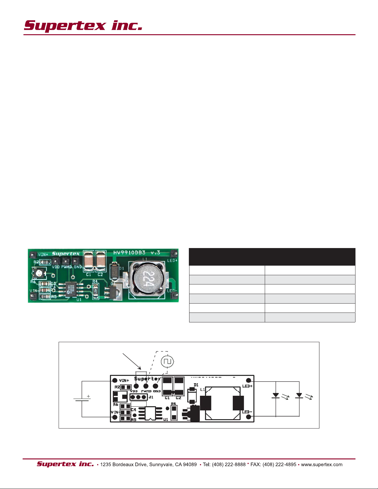
VIN+: Connect the positive terminal of the DC input source
to this pin.
VIN-: Connect the negative terminal of the DC input source
to this pin.
LED+: Connect the Anode of the LED(s) to this pin.
LED-: Connect the Cathode of the LED(s) to this pin.
VDD:This pin is connected to the VDD pin of the HV9910/
HV9910B. The typical voltage on the pin is 7.6V. This voltage
can be used to drive any additional circuitry required. Please
see the datasheet regarding the output current capability at
the VDD pin.
GND: This pin is connected to the Ground connection of the
buck converter.
PWMD: This terminal can be used to either enable/disable
the converter or to apply a PWM dimming signal.
To just enable the converter, connect the PWMD pin to the
VDD pin. Disconnecting the PWMD pin will cause the circuit
to stop.
PWM dimming of the LED light can be achieved by turning
the converter on and off with a low frequency 50Hz to 1000Hz
TTL logic level signal. Changing the Duty Ratio of the signal
changes the effective average current via the LEDs, thus
changing the light emission.
Note: In the case of PWM dimming, the PWMD pin should
not be connected to the VDD pin!
J1: The three pins in J1 are used to set the current level of
the output. The HV9910DB3v.3 has two current levels:
Pin 2 connected to Pin 1: Output Current is 900mA
Pin 2 connected to Pin 3: Output current can be adjusted
using the potentiometer
LED STRING VOLTAGE
In a constant-off time buck converter, the relationship
between the output current ripple ΔI0, the LED string voltage
V0, the inductance value L, and the programmed off time toff
is given by:
From the above equation, it can be seen that for a given value
of Land toff, the output current ripple is directly proportional
to the output voltage. A plot of the current ripple vs. the
output voltage is given below:
In cases where the current ripple is too high (as a percentage
of the average LED current), it may be necessary to add
a small ceramic capacitor between the output terminals to
reduce the LED current ripple.
Testing the HV9910DB3v.3
Connect the LED string to the output terminals. Check the
polarity of the LED connection, anode end of the string
should be connected to the positive output, cathode should
be connected to the negative output. Connect the DC input
to the input terminals (check the polarity). Short the PWMD
pin to VDD. Apply a DC voltage at the input terminals and the
LED string should start to glow.
An ammeter can be connected in series with the LED(s) to
measure the output current. The current level can then be
changed by adjusting the trimming potentiometer.
Open LED test:
After the initial test of functionality, the demo board can be
tested at open LED string. The test is non-destructive and
not time restricted. Disconnect one end of the LEDs and
power up the demo. There will be no light emission and the
AC current withdrawn from the line will be very low. There is
no switching at the switching node.
Linear dimming test:
Gradual change of current via LED(s) is possible by using
the trimming potentiometer placed on the demo board. The
HV9910 has a preset voltage reference level of 250mV when
the voltage at the LD pin of the IC is above 250mV. The
external resistor divider consisting of R2 and potentiometer
R6 can change that level by pulling down the pin LD below
250mV, reducing the LED string current in linear fashion.
The maximum output current of the HV9910DB3v.3 is about
900mA.
PWM dimming test:
During normal demo board operation, by applying a PWM
TTL level signal to pin PWMD, the output current through the
LEDs can be changed in PWM fashion in a 0 to 100% range.
In this dimming mode, the output current has normally two
levels – zero and nominal current, except at very low duty
ratios where inductor current cannot ramp up to the nominal
value within the short time.
Instructions:
VL
I
t
o
off
0=⋅
∆
0
100
200
300
400
2468
Output Voltage (V)
Current Ripple (mA)