TeleChips TCC8900 User manual

TCC8900
DEMO B’d V1.x
User’s Guide
TCC8900_DEMO_AM_2766
Rev. 1.1
July, 31, 2009

Preliminary 2
DISCLAIMER
All information and data contained in this material are without any commitment, are not to be considered as an
offer for conclusion of a contract, nor shall they be construed as to create any liability. Any new issue of this
datasheet invalidates previous issues. Product availability and delivery are exclusively subject to our respective
order confirmation form; the same applies to orders based on development samples delivered. By this publication,
Telechips, Inc. does not assume responsibility for patent infringements or other rights of third parties that may
result from its use.
No part of this publication may be reproduced, photocopied, stored on a retrieval system, or transmitted without
the express written consent of Telechips, Inc.
This product is designed for general purpose, and accordingly customer be responsible for all or any of
intellectual property licenses required for actual application. Telechips does not provide any indemnification
for any intellectual properties owned by third party.
Telechips can not ensure that this application is the proper and sufficient one for any other purposes but the
one explicitly expressed herein. Telechips is not responsible for any special, indirect, incidental or
consequential damage or loss whatsoever resulting from the use of this application for other purposes.
COPYRIGHT STATEMENT
Copyright in the material provided by Telechips is owned by Telechips unless otherwise noted.
For reproduction or use of Telechips’ copyright material, permission should be sought from Telechips. That
permission, if given, will be subject to conditions that Telechips’ name should be included and interest in the
material should be acknowledged when the material is reproduced or quoted, either in whole or in part. You must
not copy, adapt, publish, distribute or commercialize any contents contained in the material in any manner without
the written permission of Telechips. Trade marks used in Telechips’copyright material are the property of Telechips.
Important Notice
This product may include technology owned by Microsoft Corporation and in this case it cannot be used or
distributed without a license from Microsoft Licensing, GP.
For customers who use licensed Codec ICs and/or licensed codec firmware of mp3:
“Supply of this product does not convey a license nor imply any right to distribute content created with this
product in revenue-generating broadcast systems (terrestrial. Satellite, cable and/or other distribution
channels), streaming applications(via internet, intranets and/or other networks), other content distribution
systems(pay-audio or audio-on-demand applications and the like) or on physical media(compact discs,
digital versatile discs, semiconductor chips, hard drives, memory cards and the like). An independent license
for such use is required. For details, please visit http://mp3licensing.com”.
For customers who use other firmware of mp3:
“Supply of this product does not convey a license under the relevant intellectual property of Thomson and/or
Fraunhofer Gesellschaft nor imply any right to use this product in any finished end user or ready-to-use final
product. An independent license for such use is required. For details, please visit http://mp3licensing.com”.
For customers who use Digital Wave DRA solution:
“Supply of this implementation of DRA technology does not convey a license nor imply any right to this
implementation in any finished end-user or ready-to-use terminal product. An independent license for such
use is required.”

TCC8900 TCC8900_DEMO_AM_2747_V1.1 July, 31, 2009
Board Guide REVISION HISTORY
Preliminary 3
Revision History
Date Version
Description
2009-04-15 1.0
This document is a guide to the TCC8900_DEMO(CPU+MAIN)_V1.0 board
Initial release
2009-07-31 1.1
This document is a guide to the TCC8900_DEMO(CPU SV1.1+MAIN V1.1 and V1.2)
board update

TCC8900 TCC8900_DEMO_AM_2747_V1.1 July, 31, 2009
Board Guide TABLE OF CONTENTS
Preliminary 4
TABLE OF CONTENTS
Contents
1 TCC8900 Demo Board Pin Description ............................................................................................1-1
2 TCC8900 Demo Board Usage .......................................................................................................... 2-7
2.1 Jumper Setting Mode..............................................................................................................2-7
2.1.1 Boot Mode Selection............................................................................................................2-7
2.1.1 SD&MMC / MS(memory stick) Card Selection Mode........................................................2-10
2.2 NAND_CE# Setting............................................................................................................... 2-11
2.3 LCD I/F Switch Setting..........................................................................................................2-12
2.3.1 LCD I/F Switch Setting Of RGB Interface...................................................................2-12
2.3.2 LCD I/F Resistor Setting Of CPU Interface ................................................................2-12
2.4 Resistor Setting in the Non-Use of JTAG..............................................................................2-14
2.5 Switch Setting for interface function select...........................................................................2-15
3 TCC8900 Demo Board Revisions (V1.1)........................................................................................ 3-19
3.1 HDMI CEC (CPU Module).....................................................................................................3-19
3.2 Voltage Level Shift for the HDMI EDID (CPU Module) .........................................................3-19
3.3 SD1 Card (Main)...................................................................................................................3-21
3.4 GPIO Expander (Main)..........................................................................................................3-21
4 TCC8900 Demo Board Revisions (V1.2)........................................................................................ 4-22
4.1 TCC8901/8902 (Main)...........................................................................................................4-22
4.2 NAND V2 Boot Mode (Main).................................................................................................4-23
Figures
FIGURE 1. TCC8900 DEMO BOARD BLOCK DIAGRAM.............................................................................1-1
FIGURE 2. TCC8900 DEMO V1.X BOARD DESCRIPTION...........................................................................1-2
FIGURE 3. TCC8900 CPU BOARD DESCRIPTION.........................................................................................1-2
FIGURE 4. TCC8900 MAIN BOARD DESCRIPTION......................................................................................1-3
FIGURE 5. JUMPER CAP CONNECTION........................................................................................................1-6
FIGURE 6. NAND_CE# SETTING ..................................................................................................................2-11
FIGURE 7. SW12 SETTING.............................................................................................................................2-11
FIGURE 8. LCD I/F SETTING .........................................................................................................................2-12
FIGURE 9. RGB I/F LCD SWITCH SETTING................................................................................................2-12
FIGURE 10. CPU I/F LCD SWITCH SETTING ..............................................................................................2-13
FIGURE 11. 18BIT CPU I/F LCD RESISTOR SETTING................................................................................2-13
FIGURE 12. RESISTOR SETTING IN THE NON-USE OF JTAG..................................................................2-14
FIGURE 13. HDMI CEC CONTROL (SV1.1)..................................................................................................3-19
FIGURE 14. CIRCUIT OF HDMI EDID WITH CHIPSET (SV1.0).................................................................3-20
FIGURE 15. CIRCUIT OF HDMI EDID WITH THE FET (SV1.1).................................................................3-20
FIGURE 16. SD1 CARD I/F (V1.1)..................................................................................................................3-21
FIGURE 17. GPIO EXPANDER (V1.1)............................................................................................................3-21
FIGURE 18. POWER HEADER FOR TCC8901/02 (V1.2)..............................................................................4-22
FIGURE 19. XX VERSION CHIPSET (OLD)..................................................................................................4-23
FIGURE 20. AFTER AX VERSION CHIPSET (NEW)....................................................................................4-24
Tables
TABLE 1 USB BOOT MODE CONFIGURATIONS..........................................................................................2-7
TABLE 2 NAND BOOT MODE CONFIGURATIONS......................................................................................2-7
TABLE 3 I2C MASTER BOOT MODE CONFIGURATIONS...........................................................................2-8
TABLE 4 SERIAL FLASH BOOT MODE CONFIGURATIONS......................................................................2-8
TABLE 5 SPI SLAVE BOOT MODE CONFIGURATIONS...............................................................................2-8
TABLE 6 SD/MMC BOOT MODE CONFIGURATIONS..................................................................................2-9
TABLE 7 NOR FLASH BOOT MODE CONFIGURATIONS............................................................................2-9
TABLE 8 NOR FLASH BOOT MODE CONFIGURATIONS............................................................................2-9
TABLE 9 EHI BOOT MODE CONFIGURATIONS.........................................................................................2-10
TABLE 10 SD(MMC)/MS SELECTION ..........................................................................................................2-10
TABLE 11. I-POD / UART SELECTION..........................................................................................................2-15

TCC8900 TCC8900_DEMO_AM_2747_V1.1 July, 31, 2009
Board Guide TABLE OF CONTENTS
Preliminary 5
TABLE 12. SDIO WIFI / SD 4BIT SELECTION..............................................................................................2-15
TABLE 13. DXB0 / CODEC7.1 SELECTION..................................................................................................2-16
TABLE 14. CAMERA / TOUCH SCREEN SELECTION................................................................................2-17
TABLE 15. CAMERA / TOUCH SCREEN SELECTION / ETC......................................................................2-18

TCC8900 TCC8900_DEMO_AM_2747_V1.1 July, 31, 2009
Board Guide TCC8900 DEMO BOARD PIN DESCRIPTION
Preliminary 1-1
1 TCC8900 Demo Board Pin Description
1.1 TCC8900 Demo Board Block Diagram
Figure 1. TCC8900 Demo Board Block Diagram
TCC8900 TCC8900_DEMO_AM_2747_V1.1 July, 31, 2009
Board Guide TCC8900 DEMO BOARD PIN DESCRIPTION
Preliminary 1-2
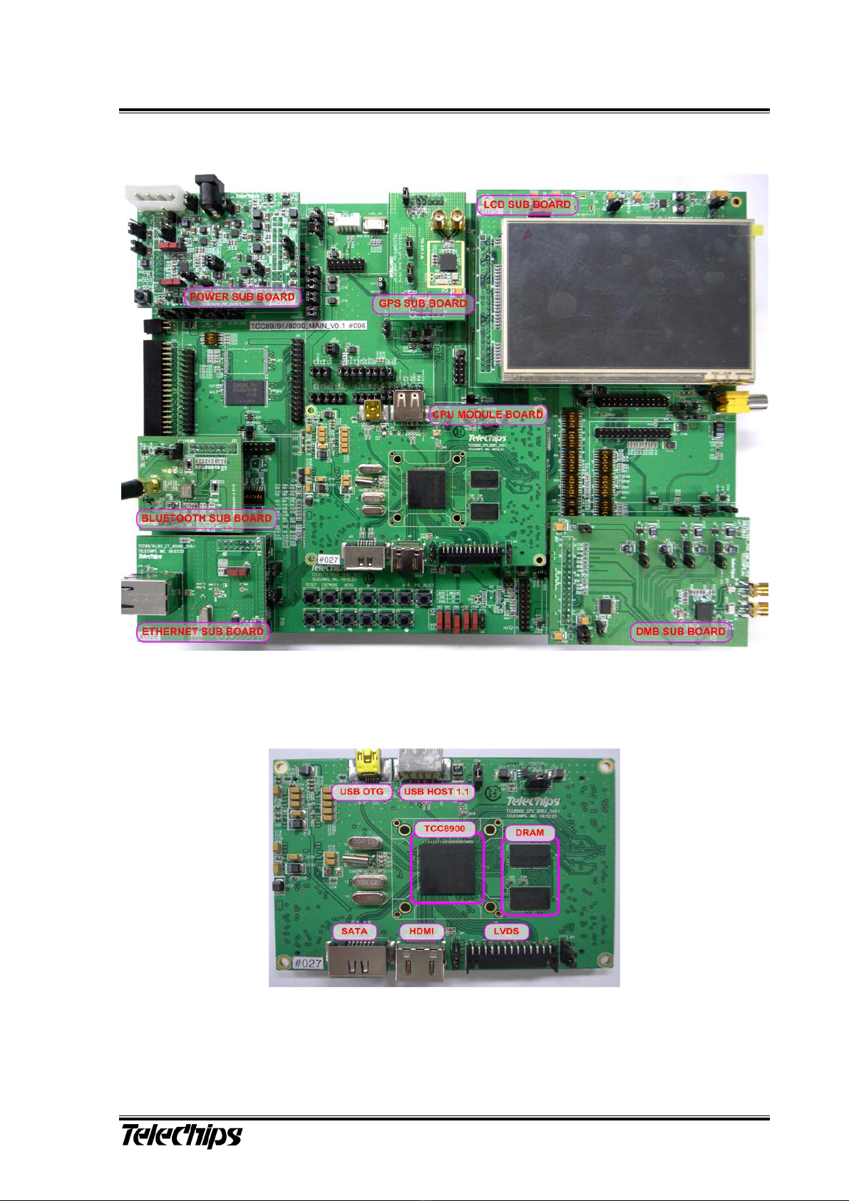
1.2 TCC8900_DEMO(CPU+MAIN) V1.x Board Description
Figure 2. TCC8900 DEMO V1.x Board Description
Figure 3. TCC8900 CPU Board Description
TCC8900 TCC8900_DEMO_AM_2747_V1.1 July, 31, 2009
Board Guide TCC8900 DEMO BOARD PIN DESCRIPTION
Preliminary 1-3
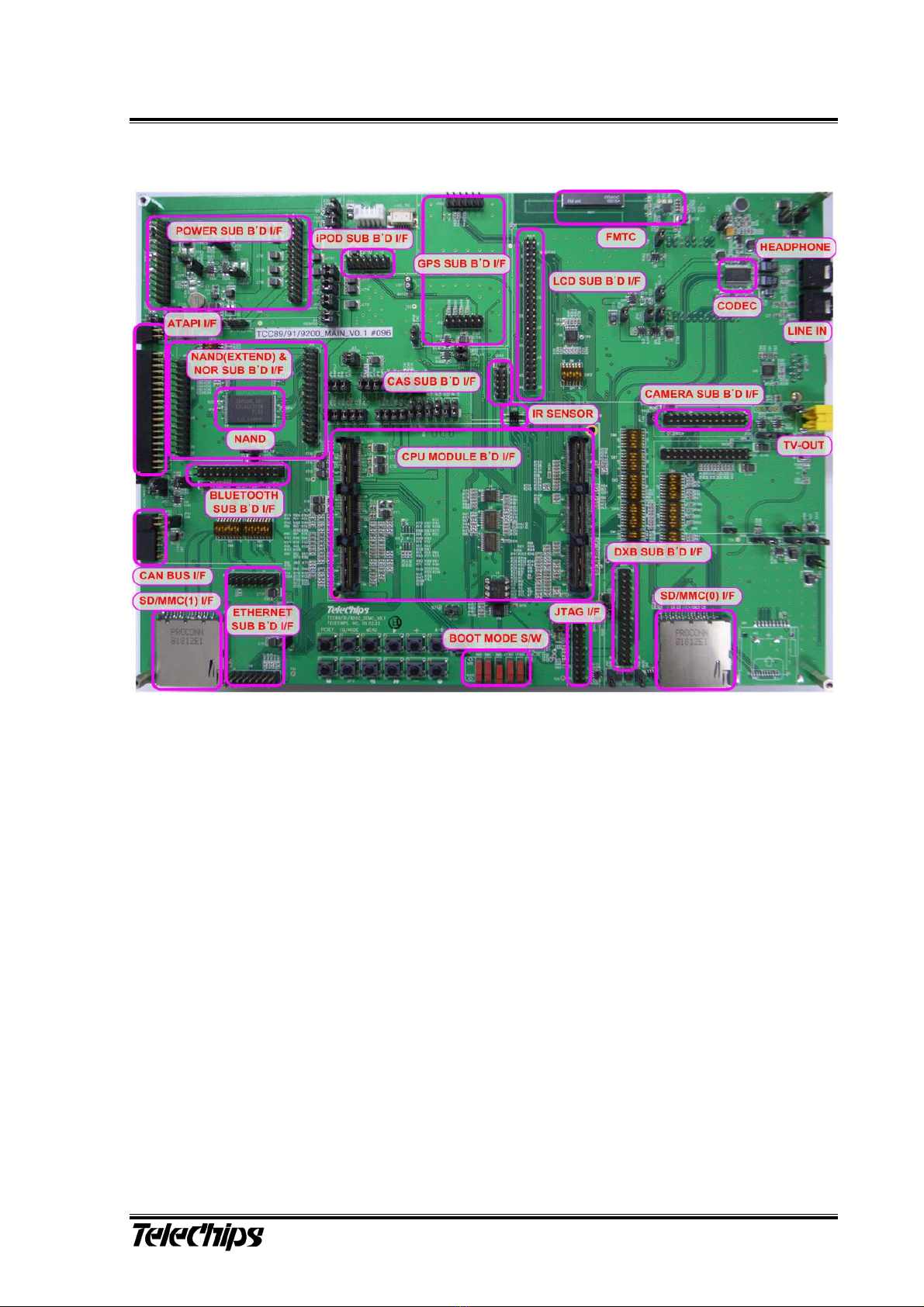
Figure 4. TCC8900 MAIN Board Description

TCC8900 TCC8900_DEMO_AM_2747_V1.1 July, 31, 2009
Board Guide TCC8900 DEMO BOARD PIN DESCRIPTION
Preliminary 1-4
zInterface Connector Description of CPU Board
-JR1: LVDS Interface Connector
-JR2: Board to Board Connector0 for Main and Module Interface
-JR3: Board to Board Connector1 for Main and Module Interface
zPower Header Pin Description of CPU Board
-JP1: HDMI_PWR
-JP2: LVDS_PWR
-JP3: DRAM_PWR
zOther Pins of CPU Board
-JC1: HDMI Connector
-JC2: USB OTG Connector
-JC3: SATAConnector
-JC4: USB Host Connector
zInterface Header Pin and Connector Description of Main Board
-JR1: Board to Board Connector0 for Main and Module Interface
-JR2: Board to Board Connector1 for Main and Module Interface
-JR8: External NAND and NOR Interface
-JR9: External NAND and NOR Interface
-JR10: ATAP Interface
-JR11: LCD Interface
-JR12: LVDS Inverter Interface
-JR13: LVDS Touch Screen Interface
-JR14: External CODEC Interface
-JR15: External CODEC Interface
-JR16: iPOD Interface
-JR17: CAB Bus Interface
-JR18: Ethernet Interface
-JR19: Ethernet Interface
-JR21: DXB Interface
-JR22: GPS Interface
-JR23: GPS Interface
-JR24: Power Interface
-JR25: Power Interface
zPower Header Pin Description of Main Board
-JP2: RTC_PWR
-JP3: CORE_PWR
-JP4: PLL_PWR
-JP5: USB12_PWR
-JP6: SATA1_PWR
-JP7: SATA2_PWR
-JP8: SATAPLL_PWR
-JP9: HDMI_PWR
-JP10: HDMIPLL1_PWR
-JP11: HDMIPLL2_PWR
-JP12: MEMQ_PWR
-JP13: MEMZQ_PWR
-JP14: GPIOA_PWR
-JP15: GPIOB_PWR

TCC8900 TCC8900_DEMO_AM_2747_V1.1 July, 31, 2009
Board Guide TCC8900 DEMO BOARD PIN DESCRIPTION
Preliminary 1-5
-JP16: GPIOC_PWR
-JP17: GPIOD_PWR
-JP18: GPIOE_PWR
-JP19: GPIOF_PWR
-JP20: OSC_PWR
-JP21: ETC_PWR
-JP22: ADC_PWR
-JP23: DAC_PWR
-JP24: USB33_PWR
-JP25: USBH_PWR
-JP26: HDMIOSC_PWR_
-JP27: LVDS33A_PWR
-JP28: SATAOSC_PWR_
-JP29: GPCNT_PWR
-JP30: NAND_PWR
-JP31: ATAPI_PWR33D
-JP32: ATAPI_PWR5D
-JP33: ATAPI_PWR5D_
-JP34: TS_PWR
-JP35: LCD_PWR
-JP36: LCD_PWR_
-JP37: CAM_PWR
-JP38: LVDS_PWR_
-JP39: MIC_PWR
-JP40: CODEC_PWR
-JP41: CODEC_18PWR
-JP42: FM_PWR
-JP43: CODEC_EXTPWR
-JP44: EM0_PWR
-JP45: EM1_PWR
-JP47: UART_PWR
-JP50: iPOD_PWR
-JP52: BT_1.8V
-JP53: BT_PWR
-JP54: CAN_PWR
-JP55: CAN_PWR_
-JP56: ETH_PWR
-JP57: GPS_PWR18
-JP58: GPS_PWR33
-JP59: GPS_PWR
-JP60: DXB_PWR28
-JP61: DXB_PWR18
-JP62: DXB_PWR12
-JP63: DXB_PWR
-JP64: GPS_GND
-JP65: GPS_GND
-JP66: DXB_PWR_
-JP67: JTAG_PWR
-JP68: DVBUS_PWR
-JP69: HVBUS_PWR
-JP70: H&L_PWR
-JP71: OTGVBUS_PWR
-JP72: SATAOSC_PWR
-JP73: HDMIOSC_PWR

TCC8900 TCC8900_DEMO_AM_2747_V1.1 July, 31, 2009
Board Guide TCC8900 DEMO BOARD PIN DESCRIPTION
Preliminary 1-6
zOther Pins of Main Board
-JP46: SDMMC_MS_SEL
-JP48: CAS_PWR_SEL
-JP51: BT_PWR_SEL
-JC1: RCA Connector
-JC2: Head Phone Connector
-JC3: Line in Connector
-JS6: JTAG_OE
zBoot Mode CS Pin
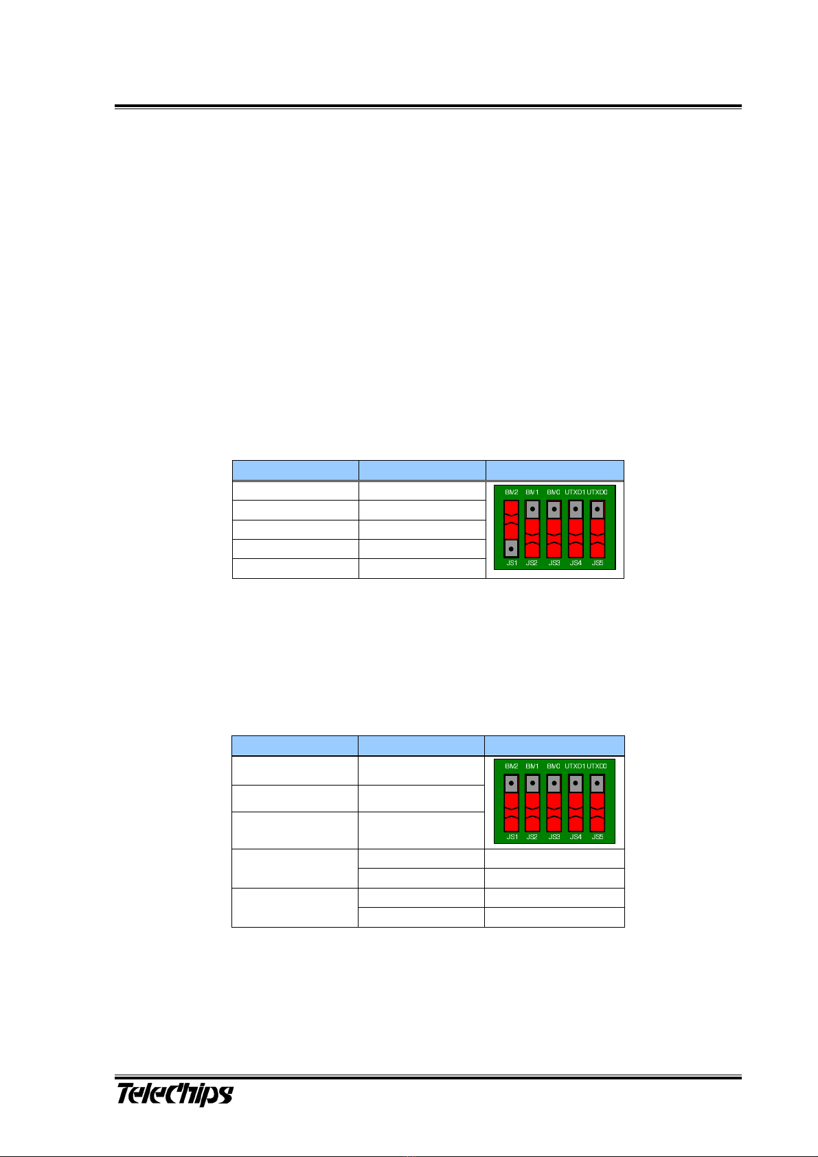
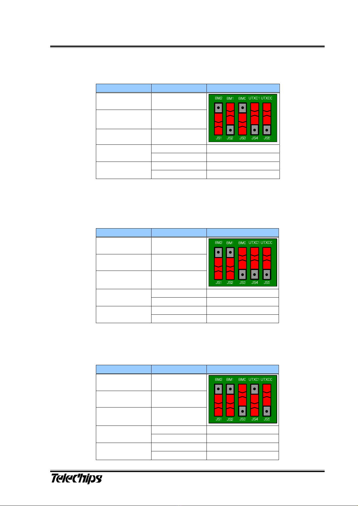
-JS1:BM2 Boot Mode 2 bit setting jumper (refer to TCC8900 datasheet)
-JS2:BM1 Boot Mode 1 bit setting jumper (refer to TCC8900 datasheet)
-JS3:BM0 Boot Mode 0 bit setting jumper (refer to TCC8900 datasheet)
-JS4:UTXD1 Boot Mode Sub 1 bit setting jumper (refer to TCC8900 datasheet)
-JS5:UTXD0 Boot Mode Sub 0 bit setting jumper (refer to TCC8900 datasheet)
JS1 ~ JS7
1-2: logical ‘High’ Switch Down
2-3: logical ‘Low’ Switch Up
Cover the jumper cap to connect pin#2 and pin#3 as can be seen in the picture below.
In opposition to jumper cap-mounting, if the slide of slide switch is pushed to the left,
the middle and the right pins are connected to each other.
Note the circles on pin #1 and pin # 3 of the slide switch.
Figure 5. Jumper Cap Connection
TCC8900 TCC8900_DEMO_AM_2747_V1.1 July, 31, 2009
Board Guide TCC8900 DEMO BOARD USAGE
Preliminary 2-7
2 TCC8900 Demo Board Usage
2.1 Jumper Setting Mode
아래 표는 TCC8900 데모 보드를 사용하기 위한 각각의 Jumper Setting Mode이다.
2.1.1 Boot Mode Selection.
TCC8900은아래 Table과같은 Boot mode가있으며, BM[2:0]와UTXD[1:0]의조합에 의해서
Boot mode가결정된다.
BM2는2bit, BM1는1bit, BM0은0bit 이며, BM은해당 Boot Mode를Selection할수있는 Slide
Switch로구성되어 있으며 Boot mode jumper setting 방법은 아래와 같다.
1) Boot from USB device (BM[2:0] - 011, UTXD[1:0] - b)- Firmware Download Mode
2) Boot from NAND Flash with CRC check (BM[2:0] - 111, UTXD[1:0] - b)
Table 1 USB Boot Mode Confi
g
urations
Pin Value Figure
BM2(JS1) Low (0)
BM1(JS2) High (1)
BM0(JS3) High (1)
UTXD1(JS4) Don’t care
UTXD0(JS5) Don’t care
Table 2 NAND Boot Mode Configurations
Pin Value Figure
BM2(JS1) High (1)
BM1(JS2) High (1)
BM0(JS3) High (1)
Low (0) GPIOB[31] - Ready
UTXD1(JS4) High (1) GPIOB[28] -Ready
Low (0) NAND V1
UTXD0(JS5) High (1) NAND V2
TCC8900 TCC8900_DEMO_AM_2747_V1.1 July, 31, 2009
Board Guide TCC8900 DEMO BOARD USAGE
Preliminary 2-8
3) Boot from I2C Master (BM[2:0] - 001, UTXD[1:0] - b)
4) Boot from Serial Flash (BM[2:0] - 010, UTXD[1:0] - b)
5) Boot from SPI Slave (BM[2:0] - 100, UTXD[1:0] - b)
Table 3 I2C Master Boot Mode Configurations
Pin Value Figure
BM2(JS1) Low (0)
BM1(JS2) Low (0)
BM0(JS3) High (1)
Low (0) I2C Ch0 Boot
UTXD1(JS4) High (1) I2C Ch1 Boot
Low (0) If I2C boot fails,
UART Ch0 boot starts.
UTXD0(JS5) High (1) If I2C boot fails,
UART Ch1 boot starts.
Table 4 Serial Flash Boot Mode Configurations
Pin Value Figure/Comment
BM2(JS1) Low (0)
BM1(JS2) High (1)
BM0(JS3) Low (0)
Low (0) If Serial flash boot fails,
UART boot starts
UTXD1(JS4) High (1) If serial flash boot fails,
USB boot starts
Low (0) In UART boot,
UART channel is 0.
UTXD0(JS5) High (1) In UART boot,
UART channel is 1.
Table 5 SPI Slave Boot Mode Configurations
Pin Value Figure
BM2(JS1) High (1)
BM1(JS2) Low (0)
BM0(JS3) Low (0)
UTXD1(JS4) Don’t care
UTXD0(JS5) High (1)
TCC8900 TCC8900_DEMO_AM_2747_V1.1 July, 31, 2009
Board Guide TCC8900 DEMO BOARD USAGE
Preliminary 2-9
6) Boot from SD/MMC (BM[2:0] - 001, UTXD[1:0] - b)
7) Boot from NOR Flash (BM[2:0] - 011, UTXD[1:0] - b)
8) Boot from UART (BM[2:0] - 011, UTXD[1:0] - b)
Table 6 SD/MMC Boot Mode Configurations
Pin Value Figure
BM2(JS1) High (1)
BM1(JS2) Low (0)
BM0(JS3) High (1)
Low (0) SD/MMC Ch0 Boot
UTXD1(JS4) High (1) SD/MMC Ch1 Boot
Low (0) Bus width 4bit
UTXD0(JS5) High (1) Bus width 1bit
Table 7 NOR Flash Boot Mode Configurations
Pin Value Figure
BM2(JS1) High (1)
BM1(JS2) High (1)
BM0(JS3) Low (0)
Low (0)
UTXD1(JS4) Low (0)
Low (0) Bus width 8bit
UTXD0(JS5) High (1) Bus width 16bit
Table 8 NOR Flash Boot Mode Configurations
Pin Value Figure
BM2(JS1) High (1)
BM1(JS2) High (1)
BM0(JS3) Low (0)
Low (0)
UTXD1(JS4) Low (0)
Low (0) UART Ch0 Boot
UTXD0(JS5) High (1) UART Ch1 Boot

TCC8900 TCC8900_DEMO_AM_2747_V1.1 July, 31, 2009
Board Guide TCC8900 DEMO BOARD USAGE
Preliminary 2-10
9) Boot from EHI (BM[2:0] - 011, UTXD[1:0] - b)
2.1.1 SD&MMC / MS(memory stick) Card Selection Mode.
위의 TABLE 1과같이 SD(MMC) Card를테스트하고자 할경우에는 JP46의1번과 2번핀을
Short시켜서 VDDIOD가인가되도록 Jumper를Setting하여 준다.
반대로, MS(memory stick) Card를테스트하고자 할경우에는 JP46의2번과 3번핀을 Short
시켜서 Low 상태가 되도록 Jumper를Setting한다.
Table 9 EHI Boot Mode Configurations
Pin Value Figure
BM2(JS1) High (1)
BM1(JS2) High (1)
BM0(JS3) Low (0)
UTXD1(JS4) Don’t care
UTXD0(JS5) Don’t care
Table 10 SD(MMC)/MS Selection
SD&MMC / MS Card Selection
SD or MMC MS (memory stick)

TCC8900 TCC8900_DEMO_AM_2747_V1.1 July, 31, 2009
Board Guide TCC8900 DEMO BOARD USAGE
Preliminary 2-11
2.2 NAND_CE# Setting
SW12
ND_CS
1
2
3
4 5
6
7
8
R25547K R25447K R25347K R25247K
ND_PWR
ND_CS#0
ND_CS#2
ND_CS#1 ND_CE#0
ND_CE#1
ND_CE#2
ND_CE#3ND_CS#3
Figure 6. NAND_CE# Setting
(A) (B) (C) (D)
Figure 7. SW12 Setting
TCC8900에서는 7개의 Chip Select를필요로 하는 NAND Flash를지원한다.
DEMO Board에는 4개의 Chip Select가가능하게 설계되었으며 Setting은다음과 같다.
1CS 방식의 NAND를사용하고자 할경우에는 FIGURE7의(A)그림과 같이 SW12의1번Pin을
On으로 Setting하여 사용하고, 2CS 방식의 NAND를사용하고자 할경우에는 (B)그림과 같이
SW12의1번과 2번핀을 모두 On으로 Setting하여 사용한다. 마찬가지로, 4CS 방식의 NAND를
사용하고자 할경우에는 (C)그림과 같이 모든 Pin을On으로 Setting하여 사용한다.
만약, TCC8900 Main Board에NAND Flash를Mount 하지 않고 Extension Header를이용하여
Nand Sub Board를사용하고자 할경우에는 FIGURE 5의(D)그림과 같이 SW12의모든 핀을
Off로Setting 하여 사용하여야 한다.
또한, 8bit 방식으로 NAND Flash를사용할 경우에는 TCC8900 Reference 회로도 상의 U6에만
NAND를Mount하고, 16bit 방식으로 사용하고자 할경우에는 U6과U7 모두에 NAND를Mount
하여 사용한다. 이때, 8bit과16bit 일때각각의 NAND Boot Mode Jumper Setting과관련해서는
위에서 설명한 바와 같이 “2.1.1 Boot Mode Selection” Part의“Table 2. NAND Boot Mode
Configurations”를참조하여 Boot Mode를Setting한다.

TCC8900 TCC8900_DEMO_AM_2747_V1.1 July, 31, 2009
Board Guide TCC8900 DEMO BOARD USAGE
Preliminary 2-12
2.3 LCD I/F Switch Setting
TCC8900 데모 보드는 아래 그림과 같이 RGB I/F용과 CPU I/F용LCD 보드를 겸용으로 사용
할수있도록 설계하였기 때문에 각각 해당되는 사용하고자 하는 LCD I/F에맞게 Switch Setting
을다르게 해주어야 한다.
현재 Default로RGB I/F용보드의 24bit LCD로Switch Setting 되어있으며, CPU I/F로사용할
경우에는 16bit LCD에맞게 Switch Setting을하면 된다.
LCD_D17
LCD_D16
LCD_OE#
LCD_AP0
LCD_CS#1
LCD_CS#0
LCD_AP2
LCD_DE
LCD_AP1
OFF ON
SW13
LCDIF_SET
1
2
3
4
5
6
12
11
10
9
8
7
Figure 8. LCD I/F Setting
따라서 CPU I/F로전환할 경우에는 Setting에맞는 Switch Select이필요하며 Setting 방법은 다
음과 같다.
2.3.1 LCD I/F Switch Setting Of RGB Interface
RGB I/F의LCD를사용할 경우에는 아래 그림과 같이 SW13의1번, 3번, 5번을 ON으로 Switch
Setting하여 사용하면 되며 8bit, 16bit, 18bit, 24bit 방식의 LCD를모두 지원한다.
Figure 9. RGB I/F LCD Switch Setting
2.3.2 LCD I/F Resistor Setting Of CPU Interface
CPU I/F의LCD를사용할 경우에는 아래 그림과 같이 SW13의2번, 4번, 6번을 ON으로 Switch
Setting하여 사용하면 된다.
TCC8900 TCC8900_DEMO_AM_2747_V1.1 July, 31, 2009
Board Guide TCC8900 DEMO BOARD USAGE
Preliminary 2-13
Figure 10. CPU I/F LCD Switch Setting
그러나 18bit CPU 방식의 LCD는사용할 경우에는 아래 그림과 같이 LCD Interface Header Parts
에구성되어 있는 Resistor를변경하면 된다.
R290 0
R289 0
LCD_CLK
LCD_VS
LCD_D16
LCD_D17
Figure 11. 18bit CPU I/F LCD Resistor Setting

TCC8900 TCC8900_DEMO_AM_2747_V1.1 July, 31, 2009
Board Guide TCC8900 DEMO BOARD USAGE
Preliminary 2-14
2.4 Resistor Setting in the Non-Use of JTAG
JTAG
TMS D17
TCK F16
TDI E16
NTRST E17
TDO B20
RTCK E15
1K
DGND
Figure 12. Resistor Setting in the Non-Use of JTAG
대부분의 Real Board (양산 보드)에서는 JTAG를사용하지 않는다. 이때의 주의할 점이 사용하지
않는 포트들에 대한 처리이다. 기본적으로 CMOS Input이나 Schmitt Trigger Input PAD가Floating
되면 I/O 과전류 발생, 시스템 오동작 등많은 문제가 발생될 수있다. 특히 JTAG 같은 경우는
시스템 전체에 영향을 미칠 수있는 부분이므로 특히 주의를 요한다. 만약, JTAG 핀들을 Floating
하고 Real Board가Noise에취약한 경우 JTAG 핀들이 순간적으로 Active 되면서 Core가JTAG에
반응하게 된다. 이로 인해 Real Board는Normal 동작 상태가 아닌 JTAG Mode로전환되며 Real
Board의외형적인 현상은 HANG(HALT)된것처럼 보이게 된다.
따라서, JTAG Block을사용하지 않을 경우 위의 Figure 14와같이 nTRST Pin을1Kohm 저항 이내
로Pull-down 처리하여 JTAG Block 전체를 Reset 상태로 유지함으로써 JTAG Block을Inactive 시
켜보드 자체의 Noise등에 의한 오동작에 대비하여야 한다.
.

TCC8900 TCC8900_DEMO_AM_2747_V1.1 July, 31, 2009
Board Guide TCC8900 DEMO BOARD USAGE
Preliminary 2-15
2.5 Switch Setting for interface function select
TCC8900의 Port는 여러 Function이 가능하게 되어 있으며 demo board에서는 동시 여러 Function
동시에 사용할 경우를 위해 Switch로 Selecting하여 각각의 Function들을 Interface할 수 있다.
한 Switch에서 Interface 가능한 Function들 중에서 한 개의 Function만을 Select하여 사용할 수
있다.
SW PIN i-POD UART GPIO
1-4 MD-DNP 필요 ON UART_TXD0 GPIO_E0
SW1
2-3 MD-DNP 필요 ON UART_RXD0 GPIO_E1
SW PIN SD WiFi SD 4Bit GPIO
1-16 ON SD1_D0
2-15 ON SDWF_D0
GPIO_B0
3-14 ON SD1_D1
4-13 ON SDWF_D1
GPIO_B1
5-12 ON SD1_D2
6-11 ON SDWF_D2
GPIO_B2
7-10 ON SD1_D3
SW2
8-9 ON SDWF_D3
GPIO_B3
1-16 ON SD1_CMD
2-15 ON SDWF_CMD
GPIO_B12
3-14 ON SD1_CLK
4-13 ON SDWF_CLK
GPIO_B13
5-12 ON SD1_WP
6-11 ON SDWF_WP
GPIO_B14
7-10 ON SD1_CD
SW6
8-9 ON SDWF_CD
GPIO_A10
Table 11. i-POD / UART Selection
Table 12. SDIO WiFi / SD 4bit Selection
Table of contents


