Tews Technologies TPCE260 User manual

TPCE260 User Manual Issue 1.0.3 Page 2 of 17
TPCE260-10R
PCI Express PMC Carrier, 5V PCI VI/O,
+12V Power Supply from PCIe Connector
TPCE260-11R
PCI Express PMC Carrier, 3.3V PCI VI/O,
+12V Power Supply from PCIe Connector
TPCE260-20R
PCI Express PMC Carrier, 5V PCI VI/O,
+12V Power Supply via PCIe Graphics Power
Connector
TPCE260-21R
PCI Express PMC Carrier, 3.3V PCI VI/O,
+12V Power Supply via PCIe Graphics Power
Connector
This document contains information, which is
proprietary to TEWS TECHNOLOGIES GmbH. Any
reproduction without written permission is forbidden.
TEWS TECHNOLOGIES GmbH has made any effort
to ensure that this manual is accurate and complete.
However TEWS TECHNOLOGIES GmbH reserves
the right to change the product described in this
document at any time without notice.
TEWS TECHNOLOGIES GmbH is not liable for any
damage arising out of the application or use of the
device described herein.
Style Conventions
Hexadecimal characters are specified with prefix 0x,
i.e. 0x029E (that means hexadecimal value 029E).
For signals on hardware products, an ‚Active Low’ is
represented by the signal name with # following, i.e.
IP_RESET#.
Access terms are described as:
W Write Only
R Read Only
R/W Read/Write
R/C Read/Clear
R/S Read/Set
2022 by TEWS TECHNOLOGIES GmbH
All trademarks mentioned are property of their respective owners.

TPCE260 User Manual Issue 1.0.3 Page 3 of 17
Issue Description Date
1.0.0 Initial Issue May 2011
1.0.1 General Revision August 2014
1.0.2 Added a chapter about the PI7C9X111SL PCI-to-PCIe Bridge
EEPROM, which is now mounted by default
November 2019
1.0.3 Order Options -2xR: removed the PCIe VGA power
connector adapter cable
January 2022

TPCE260 User Manual Issue 1.0.3 Page 4 of 17
Table of Contents
1 PRODUCT DESCRIPTION ........................................................................................... 6
2 TECHNICAL SPECIFICATION ..................................................................................... 7
3 HANDLING AND OPERATING INSTRUCTIONS ......................................................... 8
ESD Protection ................................................................................................................................8
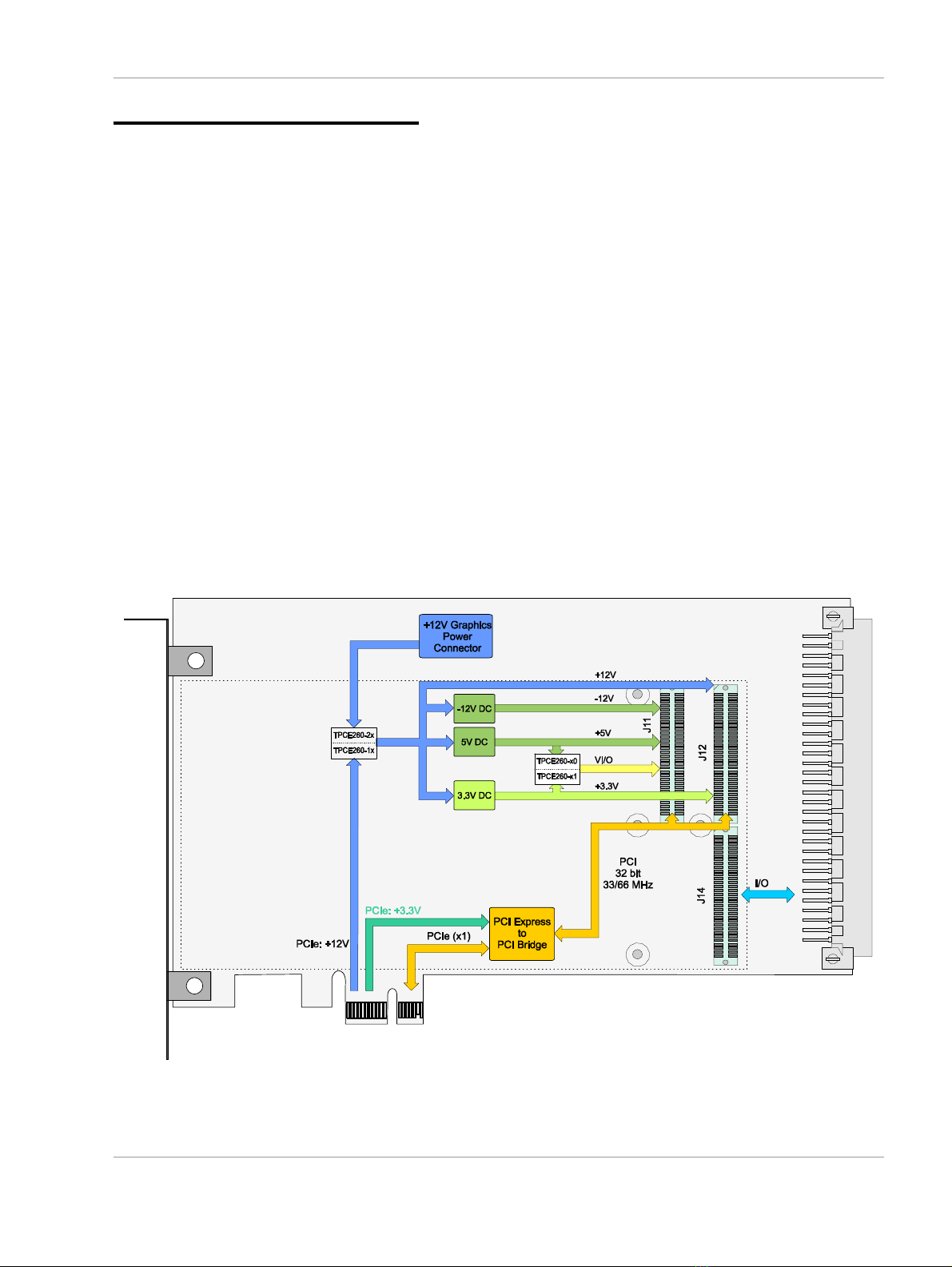
PCI Bus Signaling Voltage and Keying ........................................................................................8
Power Limits for PMC Modules .....................................................................................................8
Installation of PMC Modules ..........................................................................................................8
Installation of TPCE260-2xR ..........................................................................................................8
4 PCIE-TO-PCI BRIDGE .................................................................................................. 9
PCI Configuration Registers ..........................................................................................................9
4.1.1 PCIe-to-PCI Bridge Configuration Space Header ....................................................................9
PCI Bus Device Number Mapping ...............................................................................................10
PCI Clock Frequency ....................................................................................................................10
Configuration EEPROM................................................................................................................10
5 PMC INTERFACE ....................................................................................................... 11
PMC BUSMODE[4:1] Signals .......................................................................................................11
PCI Signaling Voltage ...................................................................................................................11
5.2.1 V_I/O Configuration ................................................................................................................11
5.2.2 Voltage Keying Configuration .................................................................................................12
Power Limits for PMC Modules ...................................................................................................13
Installation of a PMC Module .......................................................................................................13
6 PIN ASSIGNMENTS ................................................................................................... 14
PMC J11 / P11................................................................................................................................14
PMC J12 / P12................................................................................................................................15
PMC J14 / P14................................................................................................................................16
X4 VG64 Rear-I/O Connector .......................................................................................................17

TPCE260 User Manual Issue 1.0.3 Page 5 of 17
List of Figures
FIGURE 1-1 : BLOCK DIAGRAM......................................................................................................................6
FIGURE 5-1 : PCI SIGNALING VOLTAGE CONFIGURATION RESISTORS.................................................11
FIGURE 5-2 : PMC VOLTAGE KEYING ..........................................................................................................12
List of Tables
TABLE 2-1 : TECHNICAL SPECIFICATION.....................................................................................................7
TABLE 4-1 : PCIE-TO-PCI BRIDGE CONFIGURATION SPACE HEADER ....................................................9
TABLE 4-2 : PCI BUS DEVICE NUMBER MAPPING......................................................................................10
TABLE 5-1 : TPCE260 PMC BUSMODE[4:1] SIGNALS .................................................................................11
TABLE 5-2 : TPCE260 PCI SIGNALING VOLTAGE FACTORY DEFAULTS .................................................11
TABLE 5-3 : PCI SIGNALING VOLTAGE CONFIGURATION RESISTORS...................................................11
TABLE 5-4 : PCI SIGNAL VOLTAGE CONFIGURATION MATRIX.................................................................12
TABLE 5-5 : CURRENT LIMITS FOR THE PMC MODULES..........................................................................13
TABLE 6-1 : PMC J11/P11 PIN ASSIGNMENT...............................................................................................14
TABLE 6-2 : PMC J12/P12 PIN ASSIGNMENT...............................................................................................15
TABLE 6-3 : PMC J14/P14 PIN ASSIGNMENT...............................................................................................16
TABLE 6-4 : X4 VG64 PIN ASSIGNMENT ......................................................................................................17

TPCE260 User Manual Issue 1.0.3 Page 6 of 17
1 Product Description
The TPCE260 is a standard height PCI Express Revision 1.1 compatible module that provides one slot for a
single-width PMC module used to build modular, flexible and cost effective I/O solutions for all kinds of
applications like process control, medical systems, telecommunication and traffic control. The TPCE260 is a
versatile solution to upgrade well known PMC I/O solutions to the PCI Express signaling standard.
The bridging between the system host board and the PMC slot is handled by the transparent PCIe-to-PCI
Bridge PI7C9X111SL from Pericom.
The PCI bus side of the bridge allows 32-bit PCI accesses with either 33 MHz or 66 MHz. Both 3.3V (TPCE260-
x1R) and 5V (TPCE260-x0R) PCI I/O signaling voltages are supported.
The TPCE260 supports PMC front panel I/O and also PMC P14 Rear I/O through a VME P2 style connector
(IEC 60603-2, Type C). The I/O mapping of P14 complies with VITA-35 (“PMC P4 to VME-P2, Rows A-C
mapping”).
The PCIe edge card connector provides +12V and +3.3V. All TPCE260-xx variants use the +3.3V solely to
power the PCIe-to-PCI Bridge. The TPCE260-1xR uses the +12V of the PCIe edge card connector to generate
all four power supply voltages for the PMC slot (+3.3V, +5V, +12V and -12V). According to the PCIe
specification, a PCIe x1 card is limited to 6W on the +12V which allows to operate most of the available 32-bit
33/66 MHz PMC modules on the TPCE260-1xR.
For PMC modules with increased power requirements, the TPCE260-2xR offer a PCIe Graphics Power
Connector to supply the +12V for generating all the power supply voltages for the PMC slot providing a power
of up to 25W.
Figure 1-1 : Block Diagram

TPCE260 User Manual Issue 1.0.3 Page 7 of 17
2 Technical Specification
Mechanical and Electrical Interfaces
PCI Express PCI Express x1, Revision 1.1
Standard Height
Full Length
PCI (PMC Slot) PCI Mezzanine Card (PMC) Interface conforming to IEEE
P1386/P1386.1
Single Size
PCI Rev. 3.0 compliant
33/66 MHz / 32-Bit PCI
3.3V and 5V PCI Signaling Voltage
PMC Interface
Number of PMC Slots 1
PMC I/O Access PMC Front Panel I/O
PMC P14 Back I/O through VG64 Right Angle Male Connector
On Board Devices
PCI Express to PCI Bridge PI7C9X111SL (Pericom)
Physical Data
Power Requirements 250mA typical @ +3.3V DC
50mA typical @ +12V DC
Additional power is required by the PMC Module!
Maximum Power for PMC Slot TPCE260-1xR:
3 A maximum @ +3.3V DC
2 A maximum @ +5V DC
200 mA maximum @ +12V DC
200 mA maximum @ -12V DC
TPCE260-2xR:
5 A maximum @ +3.3V DC
5 A maximum @ +5V DC
200 mA maximum @ +12V DC
200 mA maximum @ -12V DC
Temperature Range Operating
Storage
-40°C to +85°C
-40°C to +85°C
MTBF TPCE260-1xR: 664000 h
TPCE260-2xR: 582000 h
MTBF values shown are based on calculation according to MIL-HDBK-217F and
MIL-HDBK-217F Notice 2; Environment: GB20°C.
The MTBF calculation is based on component FIT rates provided by the
component suppliers. If FIT rates are not available, MIL-HDBK-217F and
MIL-HDBK-217F Notice 2 formulas are used for FIT rate calculation.
Humidity 5 – 95 % non-condensing
Weight TPCE260-1xR: 99 g
TPCE260-2xR: 101 g
Table 2-1 : Technical Specification

TPCE260 User Manual Issue 1.0.3 Page 8 of 17
3 Handling and Operating Instructions
ESD Protection
The TPCE260 is sensitive to static electricity. Packing, unpacking
and all other handling of the TPCE260 has to be done in an ESD/EOS
protected Area.
PCI Bus Signaling Voltage and Keying
Be sure that the TPCE260 PCI bus signal voltage configuration
matches the TPCE260 PMC slots keying pin configuration.
If PMC modules are plugged into a PCI environment where the PCI
signaling voltage does not match, damage to the equipment could
occur, voiding product warranties.
Refer to the chapter “PCI Signaling Voltage” for details.
Power Limits for PMC Modules
The PCIe specification limits the power for PCIe add-in cards. These
limitations have implications for the use of PMC modules.
Refer to the chapter “Power Limits for PMC Modules” for details.
Installation of PMC Modules
Before mounting PMC Modules on the TPCE260, be sure that the
system is powered off.
Also, follow the installation instructions in the “PMC Interface”
chapter.
Installation of TPCE260-2xR
For the TPCE260-2xR variants, it is imperative to always connect a
PCI Express VGA power connector to the TPCE260, even if no PMC
is mounted.

TPCE260 User Manual Issue 1.0.3 Page 9 of 17
4 PCIe-to-PCI Bridge
PCI Configuration Registers
4.1.1 PCIe-to-PCI Bridge Configuration Space Header
PCI CFG
Register
Address
PCI Configuration Registers Initial Values
(Hex Values)
31 24 23 16 15 8 7 0
0x00 Device ID Vendor ID E111 12D8
0x04 Status Command 0010 0000
0x08 Class Code Revision ID 060400 02
0x0C BIST Header Type Primary Latency
Timer
Cacheline Size 00 01 00 00
0x10 Reserved -
0x14 Reserved -
0x18 Secondary Latency
Timer
Subordinate Bus
Number
Secondary Bus
Number
Primary Bus
Number
00 00 00 00
0x1C Secondary Status I/O Limit I/O Base 02A0 01 01
0x20 Memory Limit Memory Base 0000 8000
0x24 Prefetchable Memory Limit Prefetchable Memory Base 0001 8001
0x28 Prefetchable Base Upper 32-Bit 00000000
0x2C Prefetchable Limit Upper 32-Bit 00000000
0x30 I/O Limit Upper 16-Bit I/O Base Upper 16-Bit 0000 0000
0x34 Reserved Capability Pointer 000000 80
0x38 Expansion ROM Base Address 00000000
0x3C Bridge Control Interrupt Pin Interrupt Line 00 00 01 00
Table 4-1 : PCIe-to-PCI Bridge Configuration Space Header

TPCE260 User Manual Issue 1.0.3 Page 10 of 17
PCI Bus Device Number Mapping
The PCI bus device number of the PMC slot is defined by configuration type translation of the PCI-Express to
PCI Bridge.
By default, the PMC slot is mapped to the bus device number 0x0.
PCI Bus Device
Number (HEX)
PCI AD Line
used as PMC
IDSEL
Purpose
0x0 16 Default IDSEL for PMC Slot
0x1
0x2
0x3
17
18
19
Not used on TPCE260
0x4 20 Optional IDSEL for PMC Slot
0x5
-
0xF
21
-
31
Not used on TPCE260
Table 4-2 : PCI Bus Device Number Mapping
PCI Clock Frequency
The TPCE260 supports 66 MHz PCI clock frequency. The actual PCI clock frequency on the TPCE260 is
configured by the plugged PMC module. If the plugged PMC module supports 66 MHz operation, the PCI bus
will operate with 66 MHz; otherwise it will operate with 33 MHz.
Configuration EEPROM
After PCIe reset, the PI7C9X111SL loads initial configuration register data from an on board configuration I2C
EEPROM. The content is a complete set of configuration parameters based on the default settings with the
subsequent modifications.
For detailed information please refer to the PI7C9X111SL manual and Errata information.
Modifications are:
Enable Lane Polarity Inversion (disabled by default)

TPCE260 User Manual Issue 1.0.3 Page 11 of 17
5 PMC Interface
PMC BUSMODE[4:1] Signals
The BUSMODE[4:1]# signals are defined in the IEEE1386 (CMC) specification and allow a host to identify the
used mezzanine card type. The TPCE260 supports PMC cards only.
The TPCE260 indicates the “PMC only” support with the signal levels presented in the table below. The PMC
card should decode these signals and drive out a logic “0” on BUSMODE1#.
Signal Logic Level
BUSMODE4# Pulled LOW
BUSMODE3# Pulled LOW
BUSMODE2# Pulled HIGH
Table 5-1 : TPCE260 PMC BUSMODE[4:1] Signals
PCI Signaling Voltage
PMC modules are specified either for 3.3V only, 5V only or universal (3.3V or 5V) PCI signaling voltage
operation.
The TPCE260 onboard V_I/O voltage level defines the PCI signaling voltage level for the TPCE260 PCI bus.
A voltage keying pin indicates the voltage level and prevents incompatible PMC modules from being plugged
onto the carrier.
TPCE260 V_I/O Configuration 5V Keying Pin 3.3V Keying Pin
-x0 5V Installed Not Installed
-x1 3.3V Not Installed Installed
Table 5-2 : TPCE260 PCI Signaling Voltage Factory Defaults
5.2.1 V_I/O Configuration
The V_I/O signaling voltage level is configured by three resistors. To change the voltage level, these resistors
must be soldered to the appropriate soldering terminals. They are grouped and labeled appropriately.
Figure 5-1 : PCI Signaling Voltage
Configuration Resistors
TPCE260 V_I/O Populated
Resistors
Unpopulated
Resistors
5V
R500,
R501,
R502
R300,
R301,
R302
3.3V
R300,
R301,
R302
R500,
R501,
R502
Table 5-3 : PCI Signaling Voltage Configuration Resistors

TPCE260 User Manual Issue 1.0.3 Page 12 of 17
5.2.2 Voltage Keying Configuration
To prevent a PMC module from being plugged into a PMC system with a different PCI signaling voltage, the
PMC specification defines a voltage keying system with keying pins (on the PMC carrier board) and keying
holes (on the PMC module).
PMC modules supporting only 5V PCI signaling voltage provide a single keying hole for the 5V keying pin.
PMC modules supporting only 3.3V PCI signaling voltage provide a single keying hole for the 3.3V keying pin.
Universal PMC modules supporting both 3.3V and 5V PCI signaling voltages provide keying holes for both
voltage keying pins.
In certain system configurations it may be necessary to remove the keying pin from one location and assemble
it at the other keying pin location.
3.3V
Keying Pin
5V
Keying Pin
Figure 5-2 : PMC Voltage Keying
Use the following table to identify the required TPCE260 voltage keying for the actual PMC modules that are
to be used.
PMC
PCI Signaling
Voltage Capability
TPCE260 V_I/O
Configuration
TPCE260 5V
Keying Pin
TPCE260 3.3V
Keying Pin
3.3V only 3.3V Not Installed Installed
3.3V or 5V 3.3V Not Installed Installed
5V Installed Not Installed
5V only 5V Installed Not Installed
Table 5-4 : PCI Signal Voltage Configuration Matrix

TPCE260 User Manual Issue 1.0.3 Page 13 of 17
Power Limits for PMC Modules
The following current limits have to be taken into account when choosing the appropriate TPCE260 for the
power requirements of the PMC module.
TPCE260 Voltage Current Limits
TPCE260-1xR
+3.3V 3 A
+5V 2 A
+12V 200 mA
-12V 200 mA
TPCE260-2xR
+3.3V 5 A
+5V 5 A
+12V 200 mA
-12V 200 mA
Table 5-5 : Current Limits for the PMC Modules
Installation of a PMC Module
The PMC modules are mounted to the TPCE260 prior to installation into the system.
If the PMC has a front panel, first remove the cover from the PMC front panel cut-out of the TPCE260. Install
the PMC at an angle so that the PMC front panel penetrates the PMC front panel cut-out. Then rotate down to
mate with the PMC connectors on the TPCE260. If the PMC has no front panel, simply plug in the PMC, and
leave the cover in the PMC front panel cut-out of the TPCE260.
After the PMC module has been installed, it can be mounted on the TPCE260 using the mounting screws that
come with the PMC module. There are four screw mounting locations, two at the PMC front panel and two at
the standoffs near the PMC bus connectors.
Before installing a PMC module, be sure that the power supply for the TPCE260 is turned off.
The components are Electrostatic Sensitive Devices (ESD). Use an anti-static mat connected to
a wristband when handling or installing the components.
WARNING!!!
Be sure that the TPCE260 PCI bus signaling voltage (V_I/O) configuration matches the TPCE260
PMC slots keying pin configuration.
Be sure that the used PMC modules match the TPCE260 PCI bus signaling voltage and PMC slot
keying pin configuration.
If PMC modules are plugged into a PCI environment where the PCI signaling voltage does not
match, damage to the equipment could occur, voiding product warranties.

TPCE260 User Manual Issue 1.0.3 Page 14 of 17
6 Pin Assignments
PMC J11 / P11
Pin Signal Signal Pin
1 TCK -12V 2
3 GND INTA# 4
5 INTB# INTC# 6
7 BUSMODE1# +5V 8
9 INTD# PCI-RSVD 10
11 GND 3.3Vaux 12
13 CLK GND 14
15 GND GNT# 16
17 REG# +5V 18
19 V (I/O) AD[31] 20
21 AD[28] AD[27] 22
23 AD[25] GND 24
25 GND C/BE[3]# 26
27 AD[22] AD[21] 28
29 AD[19] +5V 30
31 V (I/O) AD[17] 32
33 FRAME# GND 34
35 GND IRDY# 36
37 DEVSEL# +5V 38
39 GND LOCK# 40
41 PCI-RSVD PCI-RSVD 42
43 PAR GND 44
45 V (I/O) AD[15] 46
47 AD[12] AD[11] 48
49 AD[09] +5V 50
51 GND C/BE[0]# 52
53 AD[06] AD[05] 54
55 AD[04] GND 56
57 V (I/O) AD[03] 58
59 AD[02] AD[01] 60
61 AD[00] +5V 62
63 GND REQ64# 64
Table 6-1 : PMC J11/P11 Pin Assignment

TPCE260 User Manual Issue 1.0.3 Page 15 of 17
PMC J12 / P12
Pin Signal Signal Pin
1 +12V TRST# 2
3 TMS TDO 4
5 TDI GND 6
7 GND PCI-RSVD 8
9 PCI-RSVD PCI-RSVD 10
11 BUSMODE2# +3.3V 12
13 RST# BUSMODE3# 14
15 +3.3V BUSMODE4# 16
17 PME# GND 18
19 AD[30] AD[29] 20
21 GND AD[26] 22
23 AD[24] +3.3V 24
25 IDSEL AD[23] 26
27 +3.3V AD[20] 28
29 AD[18] GND 30
31 AD[16] C/BE[2]# 32
33 GND PMC-RSVD 34
35 TRDY# +3.3V 36
37 GND STOP# 38
39 PERR# GND 40
41 +3.3V SERR# 42
43 C/BE[1]# GND 44
45 AD[14] AD[13] 46
47 M66EN AD[10] 48
49 AD[08] +3.3V 50
51 AD[07] PMC-RSVD 52
53 +3.3V PMC-RSVD 54
55 PMC-RSVD GND 56
57 PMC-RSVD PMC-RSVD 58
59 GND PMC-RSVD 60
61 ACK64# +3.3V 62
63 GND PMC-RSVD 64
Table 6-2 : PMC J12/P12 Pin Assignment

TPCE260 User Manual Issue 1.0.3 Page 16 of 17
PMC J14 / P14
The PMC J14 / P14 connector routes the PMC I/O lines directly to its appropriate pins. The actual signal
assignment is PMC specific.
Pin Signal Signal Pin
1 I/O 1 I/O 2 2
3 I/O 3 I/O 4 4
5 I/O 5 I/O 6 6
7 I/O 7 I/O 8 8
9 I/O 9 I/O 10 10
11 I/O 11 I/O 12 12
13 I/O 13 I/O 14 14
15 I/O 15 I/O 16 16
17 I/O 17 I/O 18 18
19 I/O 19 I/O 20 20
21 I/O 21 I/O 22 22
23 I/O 23 I/O 24 24
25 I/O 25 I/O 26 26
27 I/O 27 I/O 28 28
29 I/O 29 I/O 30 30
31 I/O 31 I/O 32 32
33 I/O 33 I/O 34 34
35 I/O 35 I/O 36 36
37 I/O 37 I/O 38 38
39 I/O 39 I/O 40 40
41 I/O 41 I/O 42 42
43 I/O 43 I/O 44 44
45 I/O 45 I/O 46 46
47 I/O 47 I/O 48 48
49 I/O 49 I/O 50 50
51 I/O 51 I/O 52 52
53 I/O 53 I/O 54 54
55 I/O 55 I/O 56 56
57 I/O 57 I/O 58 58
59 I/O 59 I/O 60 60
61 I/O 61 I/O 62 62
63 I/O 63 I/O 64 64
Table 6-3 : PMC J14/P14 Pin Assignment

TPCE260 User Manual Issue 1.0.3 Page 17 of 17
X4 VG64 Rear-I/O Connector
The PMC J14 / P14 I/O connector routes the PMC I/O lines to the VG64 Right Angle Male, Type C connector
compliant to VITA-35 (“PMC P4 to VME-P2, Rows A-C mapping”). The actual signal assignment of the PMC
J14 / P14 connector is PMC specific.
Pin Signal Signal Pin
c1 I/O 1 I/O 2 a1
c2 I/O 3 I/O 4 a2
c3 I/O 5 I/O 6 a3
c4 I/O 7 I/O 8 a4
c5 I/O 9 I/O 10 a5
c6 I/O 11 I/O 12 a6
c7 I/O 13 I/O 14 a7
c8 I/O 15 I/O 16 a8
c9 I/O 17 I/O 18 a9
c10 I/O 19 I/O 20 a10
c11 I/O 21 I/O 22 a11
c12 I/O 23 I/O 24 a12
c13 I/O 25 I/O 26 a13
c14 I/O 27 I/O 28 a14
c15 I/O 29 I/O 30 a15
c16 I/O 31 I/O 32 a16
c17 I/O 33 I/O 34 a17
c18 I/O 35 I/O 36 a18
c19 I/O 37 I/O 38 a19
c20 I/O 39 I/O 40 a20
c21 I/O 41 I/O 42 a21
c22 I/O 43 I/O 44 a22
c23 I/O 45 I/O 46 a23
c24 I/O 47 I/O 48 a24
c25 I/O 49 I/O 50 a25
c26 I/O 51 I/O 52 a26
c27 I/O 53 I/O 54 a27
c28 I/O 55 I/O 56 a28
c29 I/O 57 I/O 58 a29
c30 I/O 59 I/O 60 a30
c31 I/O 61 I/O 62 a31
c32 I/O 63 I/O 64 a32
Table 6-4 : X4 VG64 Pin Assignment
This manual suits for next models
4
Table of contents