Texas Equipment ADC14X250EVM User manual

User's Guide
SLAU625–November 2015
ADC14X250EVM Evaluation Module
This user's guide describes the characteristics, operation, and use of the ADC14X250EVM Evaluation
Module (EVM). This document includes a quick-start guide, directions for optimizing evaluation results, a
description of the software, alternate hardware configurations, and jumper, connector, and LED
descriptions.
Contents
1 Overview...................................................................................................................... 2
2 Quick Start Guide............................................................................................................ 4
3 Optimizing Evaluation Results............................................................................................ 10
4 Software Description ...................................................................................................... 11
5 Alternate Hardware Configurations ...................................................................................... 13
6 Jumper, Connector, and LED Descriptions............................................................................. 14
List of Figures
1 EVM Feature Locations..................................................................................................... 3
2 Quick Start Test Setup...................................................................................................... 5
3 HSDC Pro GUI Main Panel................................................................................................. 7
4 Data Capture Results from Quick Start Procedure...................................................................... 8
5 ADC14X250EVM GUI ..................................................................................................... 11
6 Low Level View Tab ....................................................................................................... 12
List of Tables
1 Quick Start Performance Measurements................................................................................. 8
2 Troubleshooting Tips........................................................................................................ 9
3 HSDC Pro Options for Optimal Analysis Results ...................................................................... 10
4 ADC14X250 GUI Tab Descriptions...................................................................................... 11
5 Low Level View Controls.................................................................................................. 12
6 Recommended LMK04828 Configurations ............................................................................. 13
7 Jumper Descriptions and Default Settings.............................................................................. 14
8 Connector Descriptions.................................................................................................... 14
9 LED Descriptions........................................................................................................... 14
Microsoft, Windows are registered trademarks of Microsoft Corporation.
1
SLAU625–November 2015 ADC14X250EVM Evaluation Module
Submit Documentation Feedback Copyright © 2015, Texas Instruments Incorporated

Overview
www.ti.com
1 Overview
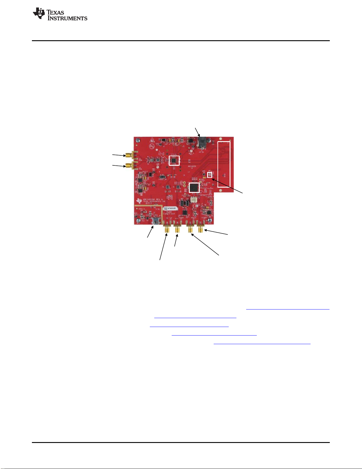
The ADC14X250EVM is an evaluation board used to evaluate the ADC14X250 analog-to-digital converter
(ADC) from Texas Instruments. The ADC14X250 is a single channel, 14-bit analog-to-digital converter
(ADC), capable of operating at sampling rates up to 250 Mega Samples Per Second (MSPS) with outputs
featuring a standard JESD204B high-speed serial interface.
This evaluation board also includes the following important features:
• Transformer-coupled signal input network allowing a single-ended signal source
• LMK04828 system clock generator that generates the FPGA reference clock for the high-speed serial
interface
• Default transformer-coupled clock input network to test the ADC performance with a very low-noise
clock
• High-speed serial data output over a standard FMC connector
• Device register programming via USB connector and FTDI USB-to-SPI bus translator
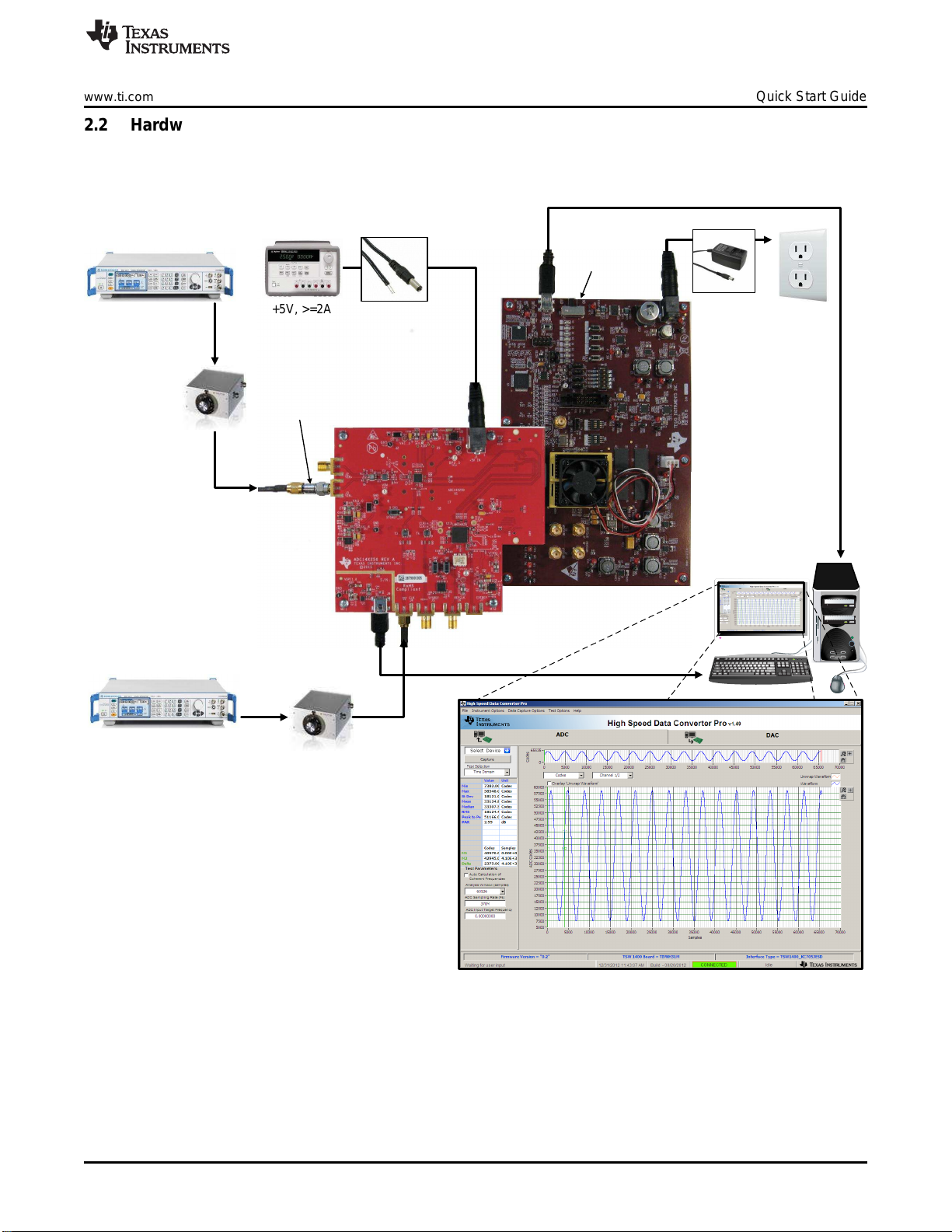
The ADC14X250EVM is designed to work seamlessly with the TSW14J56EVM, Texas Instruments’
JESD204B data capture card and the High Speed Data Converter Pro (HSDCPro) software tool for high-
speed data converter evaluation. The ADC14X250EVM is also compatible with many of the development
kits from leading FPGA vendors that contain an FMC connector.
1.1 Required Hardware
The following equipment is included in the EVM evaluation kit:
• ADC14X250EVM evaluation board (EVM)
• Flying lead-to-barrel connector power supply cable
• Mini-USB cable
The following list of equipment are items that are not included in the EVM evaluation kit but are items
required for evaluation of this product to achieve the best performance:
• TSW14J56EVM Kit: Data capture board, 5-V power supply and mini-USB cable
• 5-V power supply capable of sourcing 2 A
• Computer running Microsoft®Windows®7 or Windows XP
• Two (2) low-noise signal generators
Recommendations:
– RF generator, > 17 dBm, < –40-dBc harmonics, < 500 fs jitter 20 kHz–20 MHz, 10 MHz–2 GHz
frequency range
– Examples: TSW2170EVM, HP HP8644B, Rohde and Schwarz SMA100A
• Bandpass filter for analog input (between 125–250 MHz).
Recommendations:
– Bandpass filter, ≥60-dB harmonic attenuation, ≤5% bandwidth, > 18-dBm power, < 5-dB insertion
loss
– Examples: Trilithic 5VH-series Tunable BPF, K&L BT-series Tunable BPF, TTE KC6 or KC7-series
Fixed BPF
• Bandpass filter for clock input (250 MHz)
Recommendations:
– Bandpass filter, ≥60-dB harmonic attenuation, ≤5% bandwidth, > 18-dBm power, < 5-dB insertion
loss
– Examples: Trilithic 5VH-series Tunable BPF, K&L BT-series Tunable BPF, TTE KC6 or KC7-series
Fixed BPF
• Signal path cables, SMA and/or BNC with BNC-to-SMA adapters
2ADC14X250EVM Evaluation Module SLAU625–November 2015
Submit Documentation Feedback
Copyright © 2015, Texas Instruments Incorporated

Analog Input
ADC
USB Register
Configuration
Connector
CLK Input
FMC Connector
(Back-side)
LMK
Input Power Connector (+5V)
SYSREF Input
(Optional)
EXTREF Input
(Optional LMK04828
input reference)
SYNC
LED
VIN+
VIN-
REFCLK Input
(Optional LMK04828
output reference)
www.ti.com
Overview
1.2 Required Software
The following software is required to operate the ADC14X250EVM and available online. See the
References section for links.
• ADC14X250_GUI_Installer.zip
The following software is required to operate the TSW14J56EVM and available online. See the
Section 1.4 section for links.
•High Speed Data Converter Pro software
1.3 Evaluation Board Feature Identification Summary
Figure 1. EVM Feature Locations
1.4 References
1. ADC14X250EVM GUI software, schematics, layout, BOM, available at: www.ti.com/tool/adc14x250evm
2. ADC14X250 datasheet, available at www.ti.com/product/adc14x250
3. LMK04828 datasheet, available at www.ti.com/product/lmk04828
4. TSW14J56EVM User’s Guide, available at www.ti.com/tool/TSW14J56EVM
5. High Speed Data Converter Pro User’s Guide, available at www.ti.com/tool/dataconverterpro-sw
3
SLAU625–November 2015 ADC14X250EVM Evaluation Module
Submit Documentation Feedback Copyright © 2015, Texas Instruments Incorporated

Quick Start Guide
www.ti.com
2 Quick Start Guide
The EVM test procedure is explained in this section. Directions for obtaining a valid data capture from the
ADC14X250EVM using the TSW14J56EVM capture card are provided. This should be the starting point
for all evaluations.
2.1 Software Installation
The proper software must be installed before beginning evaluation. See the Required Software section for
a list of the required software. The References section of this document contains links to find the software
on the TI website.
CAUTION
The software must be installed before connecting the ADC14X250EVM
and TSW14J56EVM to the computer for the first time.
2.1.1 ADC14X250 GUI Installation
The ADC14X250 GUI is used to control the ADC14X250EVM. It must be used to properly configured the
devices on the EVM:
1. Download the GUI from the TI website. The Section 1.4 section of this document contains a link to find
the software on the TI website.
2. Extract the files from the .zip file.
3. Run setup.exe and follow the installation prompts.
2.1.2 High Speed Data Converter Pro GUI Installation
High Speed Data Converter Pro (HSDC Pro) is used to control the TSW14J56 and analyze the captured
data. See the HSDC Pro user’s guide (SLWU087) for more information.
1. Download the HSDC Pro from the TI website. The Section 1.4 of this document contains a link to find
the software on the TI website.
2. Extract the files from the zip file.
3. Run setup.exe and follow the installation prompts.
4ADC14X250EVM Evaluation Module SLAU625–November 2015
Submit Documentation Feedback
Copyright © 2015, Texas Instruments Incorporated

Analog
Input
6dB, 50Ÿ
Attenuator
Analog Input
Low Noise
Signal Generator
Clock Input
Low-Noise
Signal Generator
Mini-USB Cable
+5V Power Supply
70MHz
Bandpass
Filter
250MHz
Bandpass
Filter
PC Computer
Running HSDC Pro
Clock
Input
ADC EVM TSW14J56EVM
Power
Switch
OFF ON
70MHz, +10dBm
250MHz, +12dBm
Mini-USB Cable
x
x
x
x
x
x
x
x
x
x
x
x
x
x
x
x
x
x
x
x
x
x
x
x
x
x
x
x
x
x
x
x
x
x
x
x
x
x
x
x
x
x
+5V, >=2A
www.ti.com
Quick Start Guide
2.2 Hardware Setup Procedure
A typical test setup using the ADC14X250EVM and TSW14J56EVM is shown in Figure 2. This is the test
setup used for the quick-start procedure. The rest of this section describes the hardware setup steps.
Figure 2. Quick Start Test Setup
5
SLAU625–November 2015 ADC14X250EVM Evaluation Module
Submit Documentation Feedback Copyright © 2015, Texas Instruments Incorporated

Quick Start Guide
www.ti.com
2.2.1 TSW14J56EVM Setup
Setup the TSW14J56EVM with the following instructions:
1. Connect the ADC14X250EVM to the TSW14J56EVM via the FMC connectors
2. Connect the included 5-V power supply to connector J11 (+5V IN) of the TSW14J56EVM
3. Connect the included mini-USB cable to the USB connector (J9) of the TSW14J56EVM
4. Flip the power switch (SW6) of the TSW14J56EVM to the “ON” position
2.2.2 ADC14X250EVM Setup
Next, setup the ADC14X250EVM with the following instructions:
CAUTION
Check the polarity of the voltage from the power supply through the flying
lead power cable to the barrel connector at the end of the cable. 5 V must
be supplied via the center of the barrel connector on the cable. Incorrect
polarity of the power supply may damage the EVM.
1. Connect the flying lead power supply to connector J11 (+5_IN) as well as to a 5-V / 2-A bench power
supply
2. Connect the included mini-USB cable to the USB connector J9
3. Connect the 6-dB, 50-Ωattenuator to the J3 (VIN–) input
4. Set the analog input signal generator for 70 MHz, +10 dBm
5. Connect the analog input signal generator to the VIN– input. Place the bandpass filter between the
analog signal generator and the attenuator input to remove noise and harmonics from the signal
generator.
6. Set the clock input signal generator for 250 MHz, +12 dBm
7. Connect the signal generator to the CLK input. Place the bandpass filter between the clock signal
generator and the CLK input to remove noise and harmonics from the signal generator.
2.3 Software Setup Procedure
The software can be opened and configured once the hardware is properly setup.
2.3.1 ADC14X250 GUI Configuration
Configure the GUI using the following steps:
1. Open the ADC14X250 GUI by going to Start Menu →All Programs →Texas Instruments ADCs →
ADC14X250 GUI
2. Verify that the green USB status indicator is lit in the top right corner of the GUI
3. Press the ‘Program LMK04828’ button
4. Press the ‘Calibrate ADC14X250’ button
6ADC14X250EVM Evaluation Module SLAU625–November 2015
Submit Documentation Feedback
Copyright © 2015, Texas Instruments Incorporated

www.ti.com
Quick Start Guide
2.3.2 HSDC Pro GUI Configuration
Configure the HSDC Pro GUI using the following steps:
1. Open High Speed Data Converter Pro by going to Start Menu →All Programs →Texas Instruments →
High Speed Data Converter Pro.Figure 3 illustrates the GUI main page.
Figure 3. HSDC Pro GUI Main Panel
2. When prompted to select the capture board, select the TSW14J56 whose serial number corresponds
to the serial number on the TSW14J56EVM and click “OK”. This popup can be accessed through the
Instrument Options menu.
3. Select the ADC tab at the top of the GUI
4. Use the Select ADC drop-down menu at the top left corner to select ADC14X250_LMF_112
5. When prompted to update the firmware for the ADC, click “Yes” and wait for the firmware to download
to the TSW14J56
6. Enter “250M” into the ADC Output Data Rate field at the bottom left corner
7. Click the Instrument Options menu at the top of HSDC Pro and select Reset Board
8. Click “Capture” in HSDC Pro to capture data from the ADC
7
SLAU625–November 2015 ADC14X250EVM Evaluation Module
Submit Documentation Feedback Copyright © 2015, Texas Instruments Incorporated

Quick Start Guide
www.ti.com
9. The results from the captured data of Channel 1 should resemble Figure 4 and the performance
should be similar to Table 1. If this result is not achieved, then see the Quick Start Troubleshooting
section of this document.
Figure 4. Data Capture Results from Quick Start Procedure
Table 1. Quick Start Performance Measurements
Result Measured Value Unit
SNR >70.0 dBFS
SFDR >85 dBFS
8ADC14X250EVM Evaluation Module SLAU625–November 2015
Submit Documentation Feedback
Copyright © 2015, Texas Instruments Incorporated

www.ti.com
Quick Start Guide
2.4 Quick-Start Troubleshooting
Table 2 can be used to assist the user with problems that may have occurred during the quick-start
procedure.
Table 2. Troubleshooting Tips
Issue Troubleshooting Tips
Verify the test setup shown in Figure 2 and repeat the setup procedure as described in this document.
Check power supplies to the EVM and TSW14J56EVM. Verify that the power switches are in the ON
position.
Check signal and clock connections to EVM.
General Problems Check that all boards are properly connected together.
Try pressing the CPU_RESET button on the TSW14J56EVM.
Try power-cycling the external power supply to the EVM and re-programming the LMK and ADC
Devices.
Verify the settings of the configuration switches on the TSW14J56EVM.
TSW14J56 LEDs are not Verify that the EVM configuration GUI is communicating with the USB and that the configuration
correct: procedure has been followed.
D1, D5 – N/A
D2, D4 – “Blinking” (LEDs Not Blinking) Reprogram the LMK device.
D3, D6, D7 – “OFF” Try pressing the CPU_RESET button on the TSW14J56EVM.
D8, D28 – “ON” Try capturing data in HSDC Pro to force an LED status update
Verify that the USB cable is plugged into the EVM and the PC.
Check the computer’s Device Manager and verify that a ‘USB Serial Device’ is recognized when the
EVM is connected to the PC.
Device GUI is not Verify that the green ‘USB Status’ LED light in the top right corner of the GUI is lit. If it is not lit, press
working properly the ‘Reconnect FTDI’ button.
Try restarting the configuration GUI.
Check default jumper connections as shown in Section 6.
Verify that the TSW14J56EVM is properly connected to the PC with a mini-USB cable and that the
HSDC Pro Software is board serial number is properly identified by the HSDC software.
not capturing good data Check that the proper ADC device is selected. In default conditions, ‘ADC14X250_LMF_112’ should be
or analysis results are selected.
incorrect Check that the analysis parameters are properly configured.
HSDC Pro Software Try to re-program the LMK device and reset the JESD204 Link.
gives a time-out error Verify that the ADC output data rate is correct in the HSDC Pro software.
when capturing data
Press the ‘Calibrate ADC’ button on the INTRO tab or repeat the configuration GUI procedure for
programming the EVM.
Check that the spectral analysis parameters are properly configured.
Sub-Optimal Measured
Performance Verify that bandpass filters are used in the clock and input signal paths and that low-noise signal
sources are used.
Verify that an attenuator is in the signal path at the EVM VIN– input connector.
9
SLAU625–November 2015 ADC14X250EVM Evaluation Module
Submit Documentation Feedback Copyright © 2015, Texas Instruments Incorporated

Optimizing Evaluation Results
www.ti.com
3 Optimizing Evaluation Results
This section assists with optimizing the performance during evaluation of the product.
3.1 Clocking Optimization
The sampling clock provided to the ADC must have very low noise to achieve optimal results. By default,
the ADC14X250EVM is configured to require a device clock from an external signal source via the CLK
SMA connector to allow for the best possible measured performance.
Filtering of the signal generator is required to remove broadband noise and non-harmonic spurs. Narrow-
band filters are recommended to remove as much noise as possible. If a signal generator output is used
directly without filtering, significant degradation in SNR will result.
Measure the power of the clock signal at the EVM clock input (50-Ωinput). Optimize the clock amplitude
so that it is as large as possible without exceeding the maximum voltage swing specified in the datasheet
(SLASE49). This maximizes the clock edge rate giving better SNR. The insertion loss of the filter in the
clock signal path can significantly impact the voltage swing at the ADC clock input.
3.2 Coherent Input Source
A Rectangular window function can be applied to the captured data when the sample rate and the input
frequency are set precisely to capture an integer number of cycles of the input frequency (referrer to as a
coherent frequency). The clock and analog inputs must be frequency locked (such as through 10-MHz
references) in order to achieve coherency. If this cannot be achieved, then a window function like
Blackman must be applied to the data for fast-Fourier transform (FFT) analysis in the HSDC Pro Software.
3.3 HSDC Pro Settings
The HSDC Pro options highlighted in Table 3 can help improve the performance measurements.
Table 3. HSDC Pro Options for Optimal Analysis Results
HSDC Pro Feature Description
Analysis Window Selects the number of samples to include in the selected test analysis. Collect more data to improve
(samples) frequency resolution of FFT analysis.
Data Windowing Select the desired windowing function applied to the data for FFT analysis. Select ‘Blackman’ when
Function sampling a non-coherent input signal or ‘Rectangle’ when sampling a coherent input signal.
Test Options →Select bins to be removed from the spectrum and back-filled with the average noise level. One may also
Notch Frequency Bins customize the harmonics and spurs that are considered in SNR and THD calculations and select the
method for calculating spur power.
Test Options →Enable markers to narrow the Single-Tone FFT test analysis to a specific bandwidth.
Bandwidth Integration
Markers
Data Capture Options→Configure the number of contiguous samples per capture (capture depth). May also enable Continuous
Capture Options Capture and FFT Averaging.
10 ADC14X250EVM Evaluation Module SLAU625–November 2015
Submit Documentation Feedback
Copyright © 2015, Texas Instruments Incorporated

www.ti.com
Software Description
4 Software Description
4.1 ADC14X250 GUI
Figure 5 shows the front page of the ADC14X250 GUI as seen upon opening the GUI. Descriptions for
each of the tabs of the GUI are shown in Table 4.
Figure 5. ADC14X250EVM GUI
Table 4. ADC14X250 GUI Tab Descriptions
Tab Description
INTRO Configure the devices on the EVM for evaluation
ADC14X250 Provides controls for ADC14X250 features that can be used to customize evaluation.
LMK04828 Provides controls for LMK04828 features that can be used to customize evaluation or setup more advanced clocking
schemes.
Low Level View Allows write and read access to all device registers and bits. Also allows loading and saving of configuration files. The
device configurations can be saved from this tab for use in the user’s system.
11
SLAU625–November 2015 ADC14X250EVM Evaluation Module
Submit Documentation Feedback Copyright © 2015, Texas Instruments Incorporated

Software Description
www.ti.com
4.2 Low Level View
The Low Level View tab, shown in Figure 6, allows configuration of the devices at the bit and field level. At
any time, the controls described in Table 5 may be used to configure or read from the device.
Table 5. Low Level View Controls
Control Description
Register Map Displays the devices on the EVM, registers for those devices, and the states of the registers.
●Selecting a register field allows bit manipulation in the Register Data section.
●The Value column shows the value of the register at the time the GUI was last updated due to a read
or write event.
Write Register Button Write to the register highlighted in the Register Map with the value in the Write Data field. This button must
be clicked after changing bits in the register data section.
Write All Button Update all registers shown in the Register Map with the values shown in the Register Map summary.
Read Register Button Read from the register highlighted in the Register Map and display the results in the Value column.
Read All Button Read from all registers in the Register Map and display current state of hardware. Also updates the
controls in the other tabs.
Load Config Button Load a Configuration File from disk and write the registers in the file.
Save Config Button Save a Configuration File to disk that contains the current register configuration.
Register Data Cluster Manipulate individual accessible bits of the register highlighted in the Register Map.
Generic Read/Write Perform a generic read or write command to the device shown in the ‘Block’ drop-down box using the
Register Buttons Address and Write Data information
Figure 6. Low Level View Tab
12 ADC14X250EVM Evaluation Module SLAU625–November 2015
Submit Documentation Feedback
Copyright © 2015, Texas Instruments Incorporated

www.ti.com
Alternate Hardware Configurations
5 Alternate Hardware Configurations
This section describes alternate hardware configurations that can be used for customized evaluation.
5.1 Clocking Options
By default, the ADC requires a clock source from an external signal generator. Optionally, the EVM may
be configured such that the ADC is provided a clock signal by the LMK04828.
5.1.1 Providing the ADC Sampling Clock from the LMK04828
The EVM may be reconfigured to route a clock from the LMK04828 to the ADC14X250 to be used as the
device clock. This configuration represents a more realistic system configuration but the data conversion
noise performance is affected by the noise of the clock signal from the LMK device. The EVM must be
changed from the default configuration in the following ways:
• Remove R40, R41
• Place R43 and R50 with 0402, 0-Ωresistors
• Remove R227
• Configure the LMK04828 to output an LVPECL clock on the DCLKout2 output
• The reference clock for the LMK04828 must be provided via the EXTREF input connector (J7)
5.1.2 Recommended LMK04828 Configurations
The LMK04828 can be used in a number of useful configurations to provide the necessary clocks for the
ADC and JESD204B interface as described in Table 6:
Table 6. Recommended LMK04828 Configurations
Mode Description
Clock distribution mode Input reference is distributed to clock outputs and the frequency is divided, if desired. Frequency
multiplication is not supported. Input reference must be provided to CLKin1 input via CLK (J4) and R21
or via EXTREF (J7).
Clock Multiplier Mode Input reference is locked to internal VCO, allowing frequency integer-N multiplication from input to
(PLL2 Only) output. Reference must be provided at OSCin input via EXTREF or on-board XO at Y3.
Jitter Cleaner and Clock Input reference is cleaned with very low bandwidth PLL1 and then multiplied to the desired frequency
Multiplier using PLL2. Reference must be provided at CLKin1 input or on-board XO at Y1/Y2. On-board VCXO at
Mode (PLL1 + PLL2) Y3 is also required.
13
SLAU625–November 2015 ADC14X250EVM Evaluation Module
Submit Documentation Feedback Copyright © 2015, Texas Instruments Incorporated

Jumper, Connector, and LED Descriptions
www.ti.com
6 Jumper, Connector, and LED Descriptions
6.1 Jumper Descriptions
The EVM jumpers are shown in Table 7 as well as the default settings for the jumpers. Use this table to
reset the EVM in the default configuration, in case of issues.
Table 7. Jumper Descriptions and Default Settings
Jumper Description Default
Setting
SW1 LMK_SYNC push-button. Can be used to initiate the LMK04828 device SYNC function. N/A
SW2 LMK_RESET push-button. Can be used to reset the LMK04828 device. N/A
SW3 SYSREF_SW push-button. Can be used to generate a SYSREF signal edge at the ADC’s SYSREF N/A
input. (Components on EVM are not fully populated for this function by default)
6.2 Connector Descriptions
The EVM connectors and their functions are described in Table 8.
Table 8. Connector Descriptions
Connector Description
J1 (+5V IN) 5 V power connector
J2 (VIN+) VIN+ analog input to ADC via transformer network. Grounded by default.
J3 (VIN–) VIN– analog input to ADC via transformer network
J4 (CLK) Sampling Clock input for ADC via transformer network
J5 (SYSREF) SYSREF input for ADC via transformer network
J6 (REFCLK) Optional reference output from LMK04828
J7 (EXTREF) Optional reference input to LMK04828 CLKin1 or OSCin inputs
J8 FMC connector that connects to data capture card
J9 USB interface connector for device configuration
6.3 LED Descriptions
The EVM LEDs are described in Table 9.
Table 9. LED Descriptions
LED Description
SYNC Indicates status of JESD204B link
OFF: JESD204B link is not established
ON: JESD204B link is established
14 ADC14X250EVM Evaluation Module SLAU625–November 2015
Submit Documentation Feedback
Copyright © 2015, Texas Instruments Incorporated

STANDARD TERMS AND CONDITIONS FOR EVALUATION MODULES
1. Delivery: TI delivers TI evaluation boards, kits, or modules, including any accompanying demonstration software, components, or
documentation (collectively, an “EVM” or “EVMs”) to the User (“User”) in accordance with the terms and conditions set forth herein.
Acceptance of the EVM is expressly subject to the following terms and conditions.
1.1 EVMs are intended solely for product or software developers for use in a research and development setting to facilitate feasibility
evaluation, experimentation, or scientific analysis of TI semiconductors products. EVMs have no direct function and are not
finished products. EVMs shall not be directly or indirectly assembled as a part or subassembly in any finished product. For
clarification, any software or software tools provided with the EVM (“Software”) shall not be subject to the terms and conditions
set forth herein but rather shall be subject to the applicable terms and conditions that accompany such Software
1.2 EVMs are not intended for consumer or household use. EVMs may not be sold, sublicensed, leased, rented, loaned, assigned,
or otherwise distributed for commercial purposes by Users, in whole or in part, or used in any finished product or production
system.
2Limited Warranty and Related Remedies/Disclaimers:
2.1 These terms and conditions do not apply to Software. The warranty, if any, for Software is covered in the applicable Software
License Agreement.
2.2 TI warrants that the TI EVM will conform to TI's published specifications for ninety (90) days after the date TI delivers such EVM
to User. Notwithstanding the foregoing, TI shall not be liable for any defects that are caused by neglect, misuse or mistreatment
by an entity other than TI, including improper installation or testing, or for any EVMs that have been altered or modified in any
way by an entity other than TI. Moreover, TI shall not be liable for any defects that result from User's design, specifications or
instructions for such EVMs. Testing and other quality control techniques are used to the extent TI deems necessary or as
mandated by government requirements. TI does not test all parameters of each EVM.
2.3 If any EVM fails to conform to the warranty set forth above, TI's sole liability shall be at its option to repair or replace such EVM,
or credit User's account for such EVM. TI's liability under this warranty shall be limited to EVMs that are returned during the
warranty period to the address designated by TI and that are determined by TI not to conform to such warranty. If TI elects to
repair or replace such EVM, TI shall have a reasonable time to repair such EVM or provide replacements. Repaired EVMs shall
be warranted for the remainder of the original warranty period. Replaced EVMs shall be warranted for a new full ninety (90) day
warranty period.
3Regulatory Notices:
3.1 United States
3.1.1 Notice applicable to EVMs not FCC-Approved:
This kit is designed to allow product developers to evaluate electronic components, circuitry, or software associated with the kit
to determine whether to incorporate such items in a finished product and software developers to write software applications for
use with the end product. This kit is not a finished product and when assembled may not be resold or otherwise marketed unless
all required FCC equipment authorizations are first obtained. Operation is subject to the condition that this product not cause
harmful interference to licensed radio stations and that this product accept harmful interference. Unless the assembled kit is
designed to operate under part 15, part 18 or part 95 of this chapter, the operator of the kit must operate under the authority of
an FCC license holder or must secure an experimental authorization under part 5 of this chapter.
3.1.2 For EVMs annotated as FCC – FEDERAL COMMUNICATIONS COMMISSION Part 15 Compliant:
CAUTION
This device complies with part 15 of the FCC Rules. Operation is subject to the following two conditions: (1) This device may not
cause harmful interference, and (2) this device must accept any interference received, including interference that may cause
undesired operation.
Changes or modifications not expressly approved by the party responsible for compliance could void the user's authority to
operate the equipment.
FCC Interference Statement for Class A EVM devices
NOTE: This equipment has been tested and found to comply with the limits for a Class A digital device, pursuant to part 15 of
the FCC Rules. These limits are designed to provide reasonable protection against harmful interference when the equipment is
operated in a commercial environment. This equipment generates, uses, and can radiate radio frequency energy and, if not
installed and used in accordance with the instruction manual, may cause harmful interference to radio communications.
Operation of this equipment in a residential area is likely to cause harmful interference in which case the user will be required to
correct the interference at his own expense.
SPACER
SPACER
SPACER
SPACER
SPACER
SPACER
SPACER
SPACER

FCC Interference Statement for Class B EVM devices
NOTE: This equipment has been tested and found to comply with the limits for a Class B digital device, pursuant to part 15 of
the FCC Rules. These limits are designed to provide reasonable protection against harmful interference in a residential
installation. This equipment generates, uses and can radiate radio frequency energy and, if not installed and used in accordance
with the instructions, may cause harmful interference to radio communications. However, there is no guarantee that interference
will not occur in a particular installation. If this equipment does cause harmful interference to radio or television reception, which
can be determined by turning the equipment off and on, the user is encouraged to try to correct the interference by one or more
of the following measures:
•Reorient or relocate the receiving antenna.
•Increase the separation between the equipment and receiver.
•Connect the equipment into an outlet on a circuit different from that to which the receiver is connected.
•Consult the dealer or an experienced radio/TV technician for help.
3.2 Canada
3.2.1 For EVMs issued with an Industry Canada Certificate of Conformance to RSS-210
Concerning EVMs Including Radio Transmitters:
This device complies with Industry Canada license-exempt RSS standard(s). Operation is subject to the following two conditions:
(1) this device may not cause interference, and (2) this device must accept any interference, including interference that may
cause undesired operation of the device.
Concernant les EVMs avec appareils radio:
Le présent appareil est conforme aux CNR d'Industrie Canada applicables aux appareils radio exempts de licence. L'exploitation
est autorisée aux deux conditions suivantes: (1) l'appareil ne doit pas produire de brouillage, et (2) l'utilisateur de l'appareil doit
accepter tout brouillage radioélectrique subi, même si le brouillage est susceptible d'en compromettre le fonctionnement.
Concerning EVMs Including Detachable Antennas:
Under Industry Canada regulations, this radio transmitter may only operate using an antenna of a type and maximum (or lesser)
gain approved for the transmitter by Industry Canada. To reduce potential radio interference to other users, the antenna type
and its gain should be so chosen that the equivalent isotropically radiated power (e.i.r.p.) is not more than that necessary for
successful communication. This radio transmitter has been approved by Industry Canada to operate with the antenna types
listed in the user guide with the maximum permissible gain and required antenna impedance for each antenna type indicated.
Antenna types not included in this list, having a gain greater than the maximum gain indicated for that type, are strictly prohibited
for use with this device.
Concernant les EVMs avec antennes détachables
Conformément à la réglementation d'Industrie Canada, le présent émetteur radio peut fonctionner avec une antenne d'un type et
d'un gain maximal (ou inférieur) approuvé pour l'émetteur par Industrie Canada. Dans le but de réduire les risques de brouillage
radioélectrique à l'intention des autres utilisateurs, il faut choisir le type d'antenne et son gain de sorte que la puissance isotrope
rayonnée équivalente (p.i.r.e.) ne dépasse pas l'intensité nécessaire à l'établissement d'une communication satisfaisante. Le
présent émetteur radio a été approuvé par Industrie Canada pour fonctionner avec les types d'antenne énumérés dans le
manuel d’usage et ayant un gain admissible maximal et l'impédance requise pour chaque type d'antenne. Les types d'antenne
non inclus dans cette liste, ou dont le gain est supérieur au gain maximal indiqué, sont strictement interdits pour l'exploitation de
l'émetteur
3.3 Japan
3.3.1 Notice for EVMs delivered in Japan: Please see http://www.tij.co.jp/lsds/ti_ja/general/eStore/notice_01.page 日本国内に
輸入される評価用キット、ボードについては、次のところをご覧ください。
http://www.tij.co.jp/lsds/ti_ja/general/eStore/notice_01.page
3.3.2 Notice for Users of EVMs Considered “Radio Frequency Products” in Japan: EVMs entering Japan may not be certified
by TI as conforming to Technical Regulations of Radio Law of Japan.
If User uses EVMs in Japan, not certified to Technical Regulations of Radio Law of Japan, User is required by Radio Law of
Japan to follow the instructions below with respect to EVMs:
1. Use EVMs in a shielded room or any other test facility as defined in the notification #173 issued by Ministry of Internal
Affairs and Communications on March 28, 2006, based on Sub-section 1.1 of Article 6 of the Ministry’s Rule for
Enforcement of Radio Law of Japan,
2. Use EVMs only after User obtains the license of Test Radio Station as provided in Radio Law of Japan with respect to
EVMs, or
3. Use of EVMs only after User obtains the Technical Regulations Conformity Certification as provided in Radio Law of Japan
with respect to EVMs. Also, do not transfer EVMs, unless User gives the same notice above to the transferee. Please note
that if User does not follow the instructions above, User will be subject to penalties of Radio Law of Japan.
SPACER
SPACER
SPACER
SPACER
SPACER

【無線電波を送信する製品の開発キットをお使いになる際の注意事項】 開発キットの中には技術基準適合証明を受けて
いないものがあります。 技術適合証明を受けていないもののご使用に際しては、電波法遵守のため、以下のいずれかの
措置を取っていただく必要がありますのでご注意ください。
1. 電波法施行規則第6条第1項第1号に基づく平成18年3月28日総務省告示第173号で定められた電波暗室等の試験設備でご使用
いただく。
2. 実験局の免許を取得後ご使用いただく。
3. 技術基準適合証明を取得後ご使用いただく。
なお、本製品は、上記の「ご使用にあたっての注意」を譲渡先、移転先に通知しない限り、譲渡、移転できないものとします。
上記を遵守頂けない場合は、電波法の罰則が適用される可能性があることをご留意ください。 日本テキサス・イ
ンスツルメンツ株式会社
東京都新宿区西新宿6丁目24番1号
西新宿三井ビル
3.3.3 Notice for EVMs for Power Line Communication: Please see http://www.tij.co.jp/lsds/ti_ja/general/eStore/notice_02.page
電力線搬送波通信についての開発キットをお使いになる際の注意事項については、次のところをご覧くださ
い。http://www.tij.co.jp/lsds/ti_ja/general/eStore/notice_02.page
SPACER
4EVM Use Restrictions and Warnings:
4.1 EVMS ARE NOT FOR USE IN FUNCTIONAL SAFETY AND/OR SAFETY CRITICAL EVALUATIONS, INCLUDING BUT NOT
LIMITED TO EVALUATIONS OF LIFE SUPPORT APPLICATIONS.
4.2 User must read and apply the user guide and other available documentation provided by TI regarding the EVM prior to handling
or using the EVM, including without limitation any warning or restriction notices. The notices contain important safety information
related to, for example, temperatures and voltages.
4.3 Safety-Related Warnings and Restrictions:
4.3.1 User shall operate the EVM within TI’s recommended specifications and environmental considerations stated in the user
guide, other available documentation provided by TI, and any other applicable requirements and employ reasonable and
customary safeguards. Exceeding the specified performance ratings and specifications (including but not limited to input
and output voltage, current, power, and environmental ranges) for the EVM may cause personal injury or death, or
property damage. If there are questions concerning performance ratings and specifications, User should contact a TI
field representative prior to connecting interface electronics including input power and intended loads. Any loads applied
outside of the specified output range may also result in unintended and/or inaccurate operation and/or possible
permanent damage to the EVM and/or interface electronics. Please consult the EVM user guide prior to connecting any
load to the EVM output. If there is uncertainty as to the load specification, please contact a TI field representative.
During normal operation, even with the inputs and outputs kept within the specified allowable ranges, some circuit
components may have elevated case temperatures. These components include but are not limited to linear regulators,
switching transistors, pass transistors, current sense resistors, and heat sinks, which can be identified using the
information in the associated documentation. When working with the EVM, please be aware that the EVM may become
very warm.
4.3.2 EVMs are intended solely for use by technically qualified, professional electronics experts who are familiar with the
dangers and application risks associated with handling electrical mechanical components, systems, and subsystems.
User assumes all responsibility and liability for proper and safe handling and use of the EVM by User or its employees,
affiliates, contractors or designees. User assumes all responsibility and liability to ensure that any interfaces (electronic
and/or mechanical) between the EVM and any human body are designed with suitable isolation and means to safely
limit accessible leakage currents to minimize the risk of electrical shock hazard. User assumes all responsibility and
liability for any improper or unsafe handling or use of the EVM by User or its employees, affiliates, contractors or
designees.
4.4 User assumes all responsibility and liability to determine whether the EVM is subject to any applicable international, federal,
state, or local laws and regulations related to User’s handling and use of the EVM and, if applicable, User assumes all
responsibility and liability for compliance in all respects with such laws and regulations. User assumes all responsibility and
liability for proper disposal and recycling of the EVM consistent with all applicable international, federal, state, and local
requirements.
5. Accuracy of Information: To the extent TI provides information on the availability and function of EVMs, TI attempts to be as accurate
as possible. However, TI does not warrant the accuracy of EVM descriptions, EVM availability or other information on its websites as
accurate, complete, reliable, current, or error-free.
SPACER
SPACER
SPACER
SPACER
SPACER
SPACER

SPACER
6. Disclaimers:
6.1 EXCEPT AS SET FORTH ABOVE, EVMS AND ANY WRITTEN DESIGN MATERIALS PROVIDED WITH THE EVM (AND THE
DESIGN OF THE EVM ITSELF) ARE PROVIDED "AS IS" AND "WITH ALL FAULTS." TI DISCLAIMS ALL OTHER
WARRANTIES, EXPRESS OR IMPLIED, REGARDING SUCH ITEMS, INCLUDING BUT NOT LIMITED TO ANY IMPLIED
WARRANTIES OF MERCHANTABILITY OR FITNESS FOR A PARTICULAR PURPOSE OR NON-INFRINGEMENT OF ANY
THIRD PARTY PATENTS, COPYRIGHTS, TRADE SECRETS OR OTHER INTELLECTUAL PROPERTY RIGHTS.
6.2 EXCEPT FOR THE LIMITED RIGHT TO USE THE EVM SET FORTH HEREIN, NOTHING IN THESE TERMS AND
CONDITIONS SHALL BE CONSTRUED AS GRANTING OR CONFERRING ANY RIGHTS BY LICENSE, PATENT, OR ANY
OTHER INDUSTRIAL OR INTELLECTUAL PROPERTY RIGHT OF TI, ITS SUPPLIERS/LICENSORS OR ANY OTHER THIRD
PARTY, TO USE THE EVM IN ANY FINISHED END-USER OR READY-TO-USE FINAL PRODUCT, OR FOR ANY
INVENTION, DISCOVERY OR IMPROVEMENT MADE, CONCEIVED OR ACQUIRED PRIOR TO OR AFTER DELIVERY OF
THE EVM.
7. USER'S INDEMNITY OBLIGATIONS AND REPRESENTATIONS. USER WILL DEFEND, INDEMNIFY AND HOLD TI, ITS
LICENSORS AND THEIR REPRESENTATIVES HARMLESS FROM AND AGAINST ANY AND ALL CLAIMS, DAMAGES, LOSSES,
EXPENSES, COSTS AND LIABILITIES (COLLECTIVELY, "CLAIMS") ARISING OUT OF OR IN CONNECTION WITH ANY
HANDLING OR USE OF THE EVM THAT IS NOT IN ACCORDANCE WITH THESE TERMS AND CONDITIONS. THIS OBLIGATION
SHALL APPLY WHETHER CLAIMS ARISE UNDER STATUTE, REGULATION, OR THE LAW OF TORT, CONTRACT OR ANY
OTHER LEGAL THEORY, AND EVEN IF THE EVM FAILS TO PERFORM AS DESCRIBED OR EXPECTED.
8. Limitations on Damages and Liability:
8.1 General Limitations. IN NO EVENT SHALL TI BE LIABLE FOR ANY SPECIAL, COLLATERAL, INDIRECT, PUNITIVE,
INCIDENTAL, CONSEQUENTIAL, OR EXEMPLARY DAMAGES IN CONNECTION WITH OR ARISING OUT OF THESE
TERMS ANDCONDITIONS OR THE USE OF THE EVMS PROVIDED HEREUNDER, REGARDLESS OF WHETHER TI HAS
BEEN ADVISED OF THE POSSIBILITY OF SUCH DAMAGES. EXCLUDED DAMAGES INCLUDE, BUT ARE NOT LIMITED
TO, COST OF REMOVAL OR REINSTALLATION, ANCILLARY COSTS TO THE PROCUREMENT OF SUBSTITUTE GOODS
OR SERVICES, RETESTING, OUTSIDE COMPUTER TIME, LABOR COSTS, LOSS OF GOODWILL, LOSS OF PROFITS,
LOSS OF SAVINGS, LOSS OF USE, LOSS OF DATA, OR BUSINESS INTERRUPTION. NO CLAIM, SUIT OR ACTION SHALL
BE BROUGHT AGAINST TI MORE THAN ONE YEAR AFTER THE RELATED CAUSE OF ACTION HAS OCCURRED.
8.2 Specific Limitations. IN NO EVENT SHALL TI'S AGGREGATE LIABILITY FROM ANY WARRANTY OR OTHER OBLIGATION
ARISING OUT OF OR IN CONNECTION WITH THESE TERMS AND CONDITIONS, OR ANY USE OF ANY TI EVM
PROVIDED HEREUNDER, EXCEED THE TOTAL AMOUNT PAID TO TI FOR THE PARTICULAR UNITS SOLD UNDER
THESE TERMS AND CONDITIONS WITH RESPECT TO WHICH LOSSES OR DAMAGES ARE CLAIMED. THE EXISTENCE
OF MORE THAN ONE CLAIM AGAINST THE PARTICULAR UNITS SOLD TO USER UNDER THESE TERMS AND
CONDITIONS SHALL NOT ENLARGE OR EXTEND THIS LIMIT.
9. Return Policy. Except as otherwise provided, TI does not offer any refunds, returns, or exchanges. Furthermore, no return of EVM(s)
will be accepted if the package has been opened and no return of the EVM(s) will be accepted if they are damaged or otherwise not in
a resalable condition. If User feels it has been incorrectly charged for the EVM(s) it ordered or that delivery violates the applicable
order, User should contact TI. All refunds will be made in full within thirty (30) working days from the return of the components(s),
excluding any postage or packaging costs.
10. Governing Law: These terms and conditions shall be governed by and interpreted in accordance with the laws of the State of Texas,
without reference to conflict-of-laws principles. User agrees that non-exclusive jurisdiction for any dispute arising out of or relating to
these terms and conditions lies within courts located in the State of Texas and consents to venue in Dallas County, Texas.
Notwithstanding the foregoing, any judgment may be enforced in any United States or foreign court, and TI may seek injunctive relief
in any United States or foreign court.
Mailing Address: Texas Instruments, Post Office Box 655303, Dallas, Texas 75265
Copyright © 2015, Texas Instruments Incorporated
spacer

IMPORTANT NOTICE
Texas Instruments Incorporated and its subsidiaries (TI) reserve the right to make corrections, enhancements, improvements and other
changes to its semiconductor products and services per JESD46, latest issue, and to discontinue any product or service per JESD48, latest
issue. Buyers should obtain the latest relevant information before placing orders and should verify that such information is current and
complete. All semiconductor products (also referred to herein as “components”) are sold subject to TI’s terms and conditions of sale
supplied at the time of order acknowledgment.
TI warrants performance of its components to the specifications applicable at the time of sale, in accordance with the warranty in TI’s terms
and conditions of sale of semiconductor products. Testing and other quality control techniques are used to the extent TI deems necessary
to support this warranty. Except where mandated by applicable law, testing of all parameters of each component is not necessarily
performed.
TI assumes no liability for applications assistance or the design of Buyers’ products. Buyers are responsible for their products and
applications using TI components. To minimize the risks associated with Buyers’ products and applications, Buyers should provide
adequate design and operating safeguards.
TI does not warrant or represent that any license, either express or implied, is granted under any patent right, copyright, mask work right, or
other intellectual property right relating to any combination, machine, or process in which TI components or services are used. Information
published by TI regarding third-party products or services does not constitute a license to use such products or services or a warranty or
endorsement thereof. Use of such information may require a license from a third party under the patents or other intellectual property of the
third party, or a license from TI under the patents or other intellectual property of TI.
Reproduction of significant portions of TI information in TI data books or data sheets is permissible only if reproduction is without alteration
and is accompanied by all associated warranties, conditions, limitations, and notices. TI is not responsible or liable for such altered
documentation. Information of third parties may be subject to additional restrictions.
Resale of TI components or services with statements different from or beyond the parameters stated by TI for that component or service
voids all express and any implied warranties for the associated TI component or service and is an unfair and deceptive business practice.
TI is not responsible or liable for any such statements.
Buyer acknowledges and agrees that it is solely responsible for compliance with all legal, regulatory and safety-related requirements
concerning its products, and any use of TI components in its applications, notwithstanding any applications-related information or support
that may be provided by TI. Buyer represents and agrees that it has all the necessary expertise to create and implement safeguards which
anticipate dangerous consequences of failures, monitor failures and their consequences, lessen the likelihood of failures that might cause
harm and take appropriate remedial actions. Buyer will fully indemnify TI and its representatives against any damages arising out of the use
of any TI components in safety-critical applications.
In some cases, TI components may be promoted specifically to facilitate safety-related applications. With such components, TI’s goal is to
help enable customers to design and create their own end-product solutions that meet applicable functional safety standards and
requirements. Nonetheless, such components are subject to these terms.
No TI components are authorized for use in FDA Class III (or similar life-critical medical equipment) unless authorized officers of the parties
have executed a special agreement specifically governing such use.
Only those TI components which TI has specifically designated as military grade or “enhanced plastic” are designed and intended for use in
military/aerospace applications or environments. Buyer acknowledges and agrees that any military or aerospace use of TI components
which have not been so designated is solely at the Buyer's risk, and that Buyer is solely responsible for compliance with all legal and
regulatory requirements in connection with such use.
TI has specifically designated certain components as meeting ISO/TS16949 requirements, mainly for automotive use. In any case of use of
non-designated products, TI will not be responsible for any failure to meet ISO/TS16949.
Products Applications
Audio www.ti.com/audio Automotive and Transportation www.ti.com/automotive
Amplifiers amplifier.ti.com Communications and Telecom www.ti.com/communications
Data Converters dataconverter.ti.com Computers and Peripherals www.ti.com/computers
DLP® Products www.dlp.com Consumer Electronics www.ti.com/consumer-apps
DSP dsp.ti.com Energy and Lighting www.ti.com/energy
Clocks and Timers www.ti.com/clocks Industrial www.ti.com/industrial
Interface interface.ti.com Medical www.ti.com/medical
Logic logic.ti.com Security www.ti.com/security
Power Mgmt power.ti.com Space, Avionics and Defense www.ti.com/space-avionics-defense
Microcontrollers microcontroller.ti.com Video and Imaging www.ti.com/video
RFID www.ti-rfid.com
OMAP Applications Processors www.ti.com/omap TI E2E Community e2e.ti.com
Wireless Connectivity www.ti.com/wirelessconnectivity
Mailing Address: Texas Instruments, Post Office Box 655303, Dallas, Texas 75265
Copyright © 2015, Texas Instruments Incorporated
Table of contents