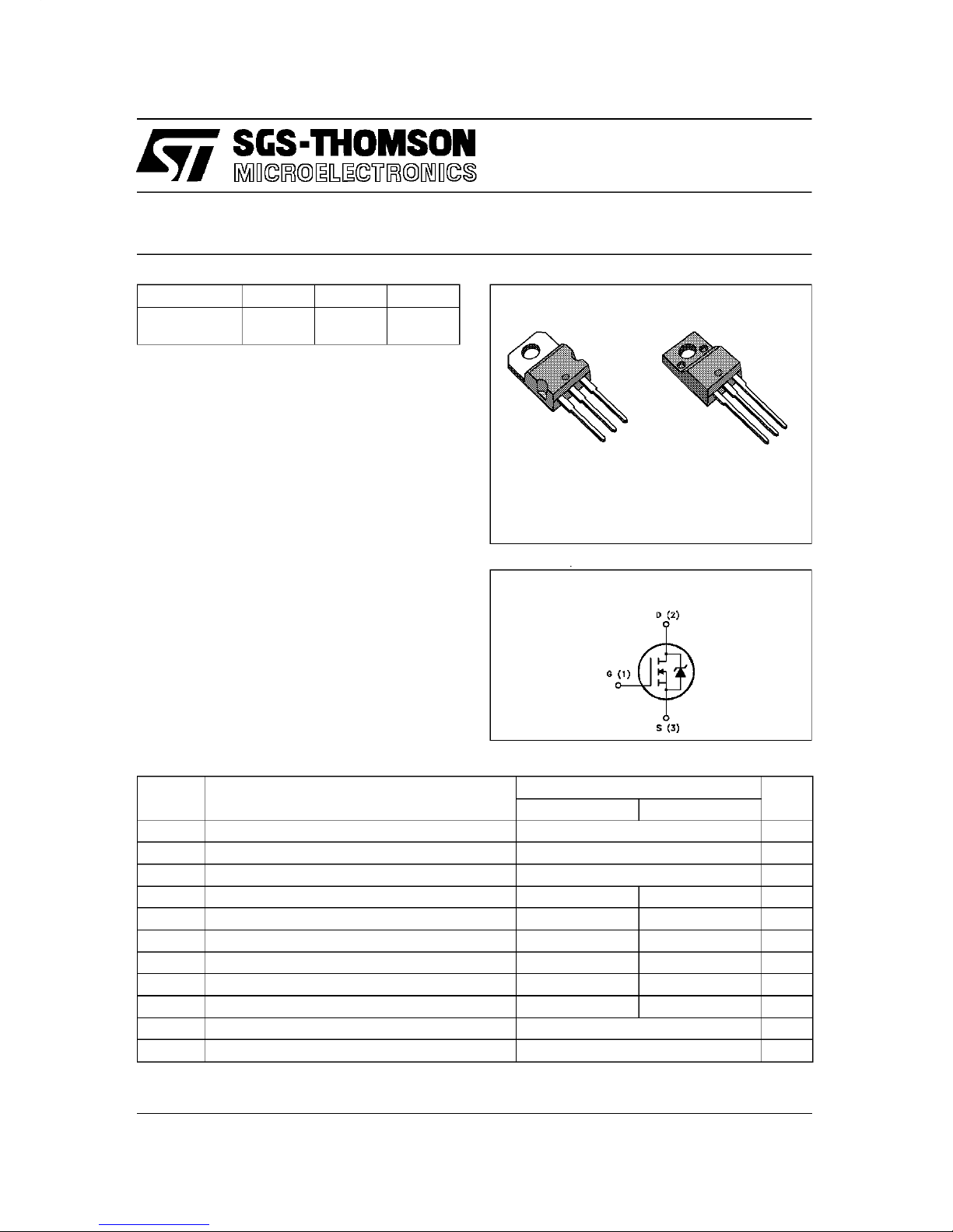
THOMSON STP6NA60 User guide

STP6NA60
STP6NA60FI
N - CHANNEL ENHANCEMENT MODE
FAST POWER MOS TRANSISTOR
■TYPICAL RDS(on) =1Ω
■±30V GATE TO SOURCE VOLTAGE RATING
■100% AVALANCHE TESTED
■REPETITIVE AVALANCHE DATA AT 100oC
■LOW INTRINSIC CAPACITANCES
■GATE GHARGE MINIMIZED
■REDUCED THRESHOLD VOLTAGE SPREAD
DESCRIPTION
This series of POWER MOSFETS represents the
most advanced high voltage technology. The
optimized cell layout coupled with a new
proprietary edge termination concur to give the
device low RDS(on) and gate charge, unequalled
ruggedness and superior switching performance.
APPLICATIONS
■HIGH CURRENT, HIGH SPEED SWITCHING
■SWITCH MODE POWERSUPPLIES (SMPS)
■DC-AC CONVERTERS FOR WELDING
EQUIPMENT AND UNINTERRUPTIBLE
POWER SUPPLIES AND MOTOR DRIVE
INTERNAL SCHEMATIC DIAGRAM
TYPE VDSS RDS(on) ID
STP6NA60
STP6NA60FI 600 V
600 V <1.2Ω
<1.2Ω6.5 A
3.9 A
123
TO-220 ISOWATT220
November 1996
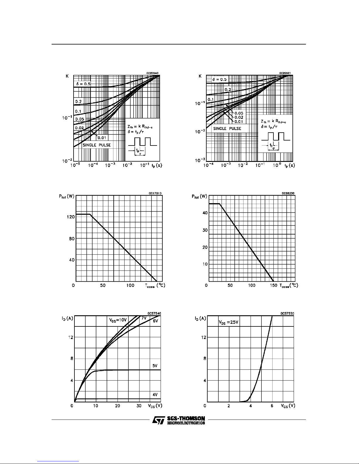
ABSOLUTE MAXIMUM RATINGS
Symbol Parameter Value Unit
STP6NA60 STP6NA60FI
VDS Drain-source Voltage (VGS =0) 600 V
V
DGR Drain-gate Voltage (RGS =20kΩ)600V
V
GS Gate-source Voltage ±30 V
IDDrain Current (continuous) at Tc=25o
C6.53.9A
I
D
Drain Current (continuous) at Tc=100o
C4.3 2.6A
I
DM(•) Drain Current (pulsed) 26 26 A
Ptot Total Dissipation at Tc=25o
C 125 45 W
Derating Factor 1 0.36 W/oC
VISO Insulation Withstand Voltage (DC) 2000 V
Tstg Storage Temperature -65 to 150 oC
TjMax. Operating Junction Temperature 150 oC
(•) Pulsewidth limited by safe operating area
123
1/10

THERMAL DATA
TO-220 ISOWATT220
Rthj-case Thermal Resistance Junction-case Max 1 2.78 oC/W
Rthj-amb
Rthc-sink
Tl
Thermal Resistance Junction-ambient Max
Thermal Resistance Case-sink Typ
Maximum Lead Temperature For Soldering Purpose
62.5
0.5
300
oC/W
oC/W
oC
AVALANCHE CHARACTERISTICS
Symbol Parameter Max Value Unit
IAR Avalanche Current, Repetitive or Not-Repetitive
(pulse width limited by Tjmax, δ <1%) 6.5 A
EAS Single Pulse Avalanche Energy
(starting Tj=25o
C, ID=I
AR,V
DD =50V) 215 mJ
EAR Repetitive Avalanche Energy
(pulse width limited by Tjmax, δ <1%) 9.5 mJ
IAR Avalanche Current, Repetitive or Not-Repetitive
(Tc= 100 oC, pulse width limited by Tjmax, δ <1%) 4.3 A
ELECTRICAL CHARACTERISTICS (Tcase =25o
C unless otherwise specified)
OFF
Symbol Parameter Test Conditions Min. Typ. Max. Unit
V(BR)DSS Drain-source
Breakdown Voltage ID=250µAV
GS = 0 600 V
IDSS Zero Gate Voltage
Drain Current (VGS =0) V
DS =MaxRating
V
DS = Max Rating x 0.8 Tc=125o
C25
250 µA
µA
IGSS Gate-body Leakage
Current (VDS =0) V
GS =±
30 V ±100 nA
ON (∗)
Symbol Parameter Test Conditions Min. Typ. Max. Unit
VGS(th) Gate Threshold Voltage VDS =V
GS ID=250µA 2.25 3 3.75 V
RDS(on) Static Drain-source On
Resistance VGS =10V I
D=3A 1 1.2 Ω
I
D(on) On State Drain Current VDS >I
D(on) xR
DS(on)max
VGS =10V 6.5 A
DYNAMIC
Symbol Parameter Test Conditions Min. Typ. Max. Unit
gfs (∗)Forward
Transconductance VDS >I
D(on) xR
DS(on)max ID=3A 3.5 5.6 S
C
iss
Coss
Crss
Input Capacitance
Output Capacitance
Reverse Transfer
Capacitance
VDS =25V f=1MHz V
GS = 0 1150
155
40
1550
210
55
pF
pF
pF
STP6NA60/FI
2/10

ELECTRICAL CHARACTERISTICS (continued)
SWITCHING ON
Symbol Parameter Test Conditions Min. Typ. Max. Unit
td(on)
trTurn-on Time
Rise Time VDD =300V I
D=3A
R
G=47
ΩV
GS =10V
(see test circuit, figure 3)
35
90 50
125 ns
ns
(di/dt)on Turn-on Current Slope VDD =480V I
D=6A
R
G=47
ΩV
GS =10V
(see test circuit, figure 5)
200 A/µs
Qg
Qgs
Qgd
Total Gate Charge
Gate-Source Charge
Gate-Drain Charge
VDD = 480 V ID=3A V
GS =10V 54
8
23
75 nC
nC
nC
SWITCHING OFF
Symbol Parameter Test Conditions Min. Typ. Max. Unit
tr(Voff)
tf
tc
Off-voltage Rise Time
Fall Time
Cross-over Time
VDD =480V I
D=6A
R
G=47
ΩV
GS =10V
(see test circuit, figure 5)
80
20
115
110
30
155
ns
ns
ns
SOURCE DRAIN DIODE
Symbol Parameter Test Conditions Min. Typ. Max. Unit
ISD
ISDM(•)Source-drain Current
Source-drain Current
(pulsed)
6.5
26 A
A
VSD (∗) Forward On Voltage ISD =6.5A V
GS =0 1.6 V
t
rr
Qrr
IRRM
Reverse Recovery
Time
Reverse Recovery
Charge
Reverse Recovery
Current
ISD =6A di/dt=100A/µs
V
DD = 100 V Tj=150o
C
(see test circuit, figure 5)
600
9
30
ns
µC
A
(∗) Pulsed: Pulse duration = 300 µs, duty cycle 1.5%
(•) Pulse width limited by safe operating area
Safe Operating Areas for TO-220 Safe Operating Areas forISOWATT220
STP6NA60/FI
3/10

Thermal Impedeance For TO-220
Derating Curve For TO-220
Output Characteristics
Thermal Impedance For ISOWATT220
Derating Curve For ISOWATT220
Transfer Characteristics
STP6NA60/FI
4/10

Transconductance Static Drain-source On Resistance
Gate Charge vs Gate-source Voltage Capacitance Variations
Normalized On Resistance vs TemperatureNormalized Gate Threshold Voltage vs
Temperature
STP6NA60/FI
5/10

Turn-on Current Slope Turn-off Drain-source Voltage Slope
Cross-over Time Switching Safe Operating Area
Accidental Overload Area Source-drain Diode Forward Characteristics
STP6NA60/FI
6/10

Fig. 2: Unclamped Inductive Waveforms
Fig. 3: Switching Times Test Circuits For
Resistive Load Fig. 4: Gate Charge Test Circuit
Fig. 5: Test Circuit For Inductive Load Switching
And Diode Reverse Recovery Time
Fig. 1: Unclamped Inductive Load Test Circuits
STP6NA60/FI
7/10

DIM. mm inch
MIN. TYP. MAX. MIN. TYP. MAX.
A 4.40 4.60 0.173 0.181
C 1.23 1.32 0.048 0.051
D 2.40 2.72 0.094 0.107
D1 1.27 0.050
E 0.49 0.70 0.019 0.027
F 0.61 0.88 0.024 0.034
F1 1.14 1.70 0.044 0.067
F2 1.14 1.70 0.044 0.067
G 4.95 5.15 0.194 0.203
G1 2.4 2.7 0.094 0.106
H2 10.0 10.40 0.393 0.409
L2 16.4 0.645
L4 13.0 14.0 0.511 0.551
L5 2.65 2.95 0.104 0.116
L6 15.25 15.75 0.600 0.620
L7 6.2 6.6 0.244 0.260
L9 3.5 3.93 0.137 0.154
DIA. 3.75 3.85 0.147 0.151
L6
A
C
D
E
D1
F
G
L7
L2
Dia.
F1
L5
L4
H2
L9
F2
G1
TO-220 MECHANICAL DATA
P011C
STP6NA60/FI
8/10

DIM. mm inch
MIN. TYP. MAX. MIN. TYP. MAX.
A 4.4 4.6 0.173 0.181
B 2.5 2.7 0.098 0.106
D 2.5 2.75 0.098 0.108
E 0.4 0.7 0.015 0.027
F 0.75 1 0.030 0.039
F1 1.15 1.7 0.045 0.067
F2 1.15 1.7 0.045 0.067
G 4.95 5.2 0.195 0.204
G1 2.4 2.7 0.094 0.106
H 10 10.4 0.393 0.409
L2 16 0.630
L3 28.6 30.6 1.126 1.204
L4 9.8 10.6 0.385 0.417
L6 15.9 16.4 0.626 0.645
L7 9 9.3 0.354 0.366
Ø 3 3.2 0.118 0.126
L2
A
B
D
E
H
G
L6
Ø
F
L3
G1
123
F2
F1
L7
L4
ISOWATT220 MECHANICAL DATA
P011G
STP6NA60/FI
9/10

Information furnished is believed to be accurate and reliable. However, SGS-THOMSON Microelectronics assumes no responsability for the
consequences of useof such informationnor for any infringement of patents or other rights of third parties which may results fromits use. No
licenseis granted by implication orotherwise underany patentor patentrights of SGS-THOMSON Microelectronics. Specifications mentioned
in this publication aresubject to change withoutnotice. Thispublication supersedes andreplacesall information previously supplied.
SGS-THOMSONMicroelectronics products are not authorized for use ascriticalcomponents in lifesupport devices or systems without express
writtenapproval ofSGS-THOMSONMicroelectonics.
1996 SGS-THOMSON Microelectronics - Printed in Italy- All Rights Reserved
SGS-THOMSONMicroelectronics GROUP OF COMPANIES
Australia - Brazil - Canada - China- France- Germany - HongKong- Italy - Japan- Korea- Malaysia - Malta - Morocco - The Netherlands -
Singapore - Spain- Sweden- Switzerland-Taiwan - Thailand- UnitedKingdom - U.S.A
.
STP6NA60/FI
10/10
This manual suits for next models
1
Table of contents