Toshiba TLP7820 User manual

RD014-RGUIDE-01
2018-03-15
Rev. 1
1/ 19
© 2018
Toshiba Electronic Devices & Storage Corporation
Isolation Amplifier
Application Circuits (Voltage Sensing)
of the TLP7820
Reference Guide
RD014-RGUIDE-01

RD014-RGUIDE-01
2018-03-15
Rev. 1
2/ 19
© 2018
Toshiba Electronic Devices & Storage Corporation
Table of Contents
1. OVERVIEW ................................................................................................... 3
1.1 Target applications ............................................................................................................ 3
2. MAJOR FEATURES OF THE TLP7820 .............................................................. 4
3. APPLICATION CIRCUIT EXAMPLE AND ITS BILL OF MATERIALS.................... 9
3.1 Example of an application circuit for voltage sensing .......................................................... 9
3.2 Bill of materials ................................................................................................................ 10
4. GUIDELINES FOR DESIGNING A VOLTAGE-SENSING CIRCUIT .................... 10
4.1 Voltage-sensing resistors in a voltage-sensing circuit ....................................................... 10
4.2 Test mode considerations ................................................................................................ 11
5. SIMULATION .............................................................................................. 11
5.1 Basic operation ................................................................................................................ 11
5.2 Noise superimposed on the input voltage ......................................................................... 13
5.3 Circuit with filters ............................................................................................................ 14
6. PRODUCT OVERVIEW ................................................................................. 16
6.1. Overview ........................................................................................................................ 16
6.2. External view and pin assignment ................................................................................... 17
6.3. Internal block diagram ................................................................................................... 17
6.4 Output voltages for different primary- and secondary-side power supply combinations .... 18

RD014-RGUIDE-01
2018-03-15
Rev. 1
3/ 19
© 2018
Toshiba Electronic Devices & Storage Corporation
1. Overview
Factory Automation (FA) market has AC servo, General Purpose Inverter, Solar Power Generation
and Wind Power Generation areas and those applicationʼs key design point is to accurate current
sense, voltage sense so that each application can realize high accuracy and stability of motions and
controls and isolation performance between input and output signals. In order to realize such kind
of high accuracy motions and controls, system has to monitor motorʼs current and voltage and
feedback them to microcontroller (MCU) more properly.
The TLP7820 is an isolation amplifier which has optical coupled isolation feature in order to meet
above requirement with 0.02% (typical) linearity accuracy. The TLP7820 also provides a common-
mode transient immunity (CMTI) of 20 kV/μs (typical), therefore stable even in noisy motor control
environments. In addition, the guaranteed isolation voltage of 5000 Vrms (minimum) makes the
TLP7820 suit various industrial applications.
In order to achieve those characteristics, the TLP7820 has a high-precision delta-sigma AD
converter at the primary side and DA converter at the secondary side. The primary and secondary
sides of the TLP7820 isolation amplifier are optically coupled using an LED and a photodiode to
provide electrical isolation and internal signal transfer of optical transfer with digital signal realizes
high accuracy signal transfer.
The delta-sigma AD converter at the primary side encodes an input analog signal into digital data,
then optically transmitted to the secondary side by an LED. At the secondary side, the optical signal
is received by a photodiode, decoded by a decoder circuit, converted back to an analog signal by a
DA converter, filtered internal conversion noise by a lowpass filter (LPF), then output analog signal
properly.
This reference guide provides the unique features and characteristics of the TLP7820, focusing on
common-mode transient immunity, nonlinearity characteristic, and power consumption, as well as
design guidelines for typical voltage-sensing applications. For details of other features and functions
of the TLP7820, see its datasheet.
To download the datasheet for the TLP7820 →
1.1 Target applications
Voltage sensing for industrial motor applications, including inverters, servo amplifiers, robots,
machine tools, and high-capacity power supplies
Voltage sensing for wind power and PV inverters, and industrial storage battery systems
Voltage sensing for office and housing equipment, including uninterruptible power supplies
(UPS), server power supplies, home storage battery systems, and air conditioners
Click Here

RD014-RGUIDE-01
2018-03-15
Rev. 1
4/ 19
© 2018
Toshiba Electronic Devices & Storage Corporation
Example of an application to an inverter
* Toshiba offers the TLP5214A photocoupler suitable for use as an IGBT gate driver.
For details of the TLP5214A →
2. Major features of the TLP7820
Common-mode transient immunity (CMTI)
Common-mode noise is a type of electrical noise that overlaps on both signal and GND lines in
the same direction. A photocoupler is used to optically transmit a signal between two isolated
circuits with independent power supplies, however even in this case, a common-mode noise is
generated by changes in the voltage of either one of the power supplies (for example, input a
noise from outside). A common-mode noise generates a displacement current to flow through
the internal coupling capacitance between the primary (input) and secondary (output) sides of
a photocoupler and if a displacement current excees a given level into coupling capacitor, the
photocoupler has malfunction, then resulting in faulty system operation.
A displacement current generated by transient common-mode noise could cause bit errors in
an isolation amplifier, in the worst-case, it leads to a short-circuit failure of an IGBT. There fore
it is important for stable system operations to tolerate common-mode noise. CMTI indicates the
ability of an isolation amplifier to tolerate high-slew-rate transient voltage induced across GND
lines. An isolation amplifier with a high CMTI provides high immunity to common-mode noise
and is suit applications requiring electrical isolation.
Click Here

RD014-RGUIDE-01
2018-03-15
Rev. 1
5/ 19
© 2018
Toshiba Electronic Devices & Storage Corporation
Figure 2.1 shows an example of a test circuit for measuring the output waveform with a common-
mode voltage (VCM) applied.
Figure 2.1 Example of a test circuit for measuring the output waveform with a
common-mode voltage (VCM) applied
An inverter contains discrete IGBT (or IGBT module) with a collector-emitter voltage (VCE) of
600 to 650V or 1200V. The 600V to 650V IGBTs are generally used at a supply voltage of 400V,
and 1200V IGBTs are commonly used at 800V. Typically, IGBTs have rise and fall times (tr and
tf) of roughly 100ns when switching. Under these conditions, the slew rate (dV/dt) of VCM is
calculated to be 4kV/μs at a supply voltage of 400V and 8kV/μs at 800V. Figure 2.2 shows
examples of output waveforms of the TLP7820 when common-mode voltages (VCM) with 4-kV/μs
and 8-kV/μs slew rates are applied. As shown in Figure 2.2, VOUT does not have much noise,
which proves that the TLP7820 has enough CMTI performance to apply actual applications.
A)When dV/dt = 4 kV/μs B)When dV/dt = 8 kV/μs
Figure 2.2 Example of output waveforms of the TLP7820 with common-mode voltages
(VCM) applied
VCM
(VOUT+) - (VOUT-)
VCM: 1 kV/div
dV/dt = 4 kV/μs
(VOUT+) - (VOUT-): 100 mV/div
t: 80 ns/div
VCM
(VOUT+) - (VOUT-)
VCM: 1 kV/div
dV/dt = 8kV/μs
(VOUT+) - (VOUT-): 100 mV/div
t: 80 ns/div

RD014-RGUIDE-01
2018-03-15
Rev. 1
6/ 19
© 2018
Toshiba Electronic Devices & Storage Corporation
Just for reference, Figure 2.3 shows an example of an output waveform when the common-
mode voltage VCM has a very large dV/dt rate with 60kV/μs. The VOUT waveform has a noise
spike caused by VCM sudden change. This noise spike could cause a total system malfunction if
it becomes larger.
Figure 2.3 Example of an output waveform of the TLP7820 when a common-mode
voltage (VCM) with a very large slew rate is applied
About output linearity characteristics
When system feedback needs using isolation amplifier detecting current fluctuations, it is
important for input-output linearity characteristics to control system properly. The output of an
isolation amplifier with bad linearity characteristics does not respond accurately with specific
input so there are lacking of the stability and accuracy of a system. In the trend of increasing
speed, accurate control is required for inverters and it is important for isolation amplifier to
minimize the output errors. Although an electronic circuit or software can be used to correct
output errors, both methods are impractically complicated and difficult, considering variations
in device characteristics. Using an isolation amplifier with high precision linearity characteristics
is more practical. Figure 2.4 shows a test circuit for measuring the linearity characteristics of
an isolation amplifier.
Figure 2.4 Example of a nonlinearity test circuit
VCM
(VOUT+) - (VOUT-)
VCM: 1 kV/div
dV/dt = 60 kV/μs
t: 80 ns/div
(VOUT+) - (VOUT-): 100 mV/div

RD014-RGUIDE-01
2018-03-15
Rev. 1
7/ 19
© 2018
Toshiba Electronic Devices & Storage Corporation
The NL200 or NL100 parameter represents the linearity of an isolation amplifier. NL200 is
calculated as follows:
1. The least-squares method is used to find a line of the best fit that represents the
relationship between the input voltage differential (VIN+-VIN-) and the output voltage
differential (VOUT+-VOUT-).
2. The deviations of the output voltage differential (VOUT+-VOUT-) from the line of the best
fit are calculated.
3. The sum of the absolute values of the maximum and minimum deviations
(|dev_max|+|dev_min|) is calculated.
4. The ratio of this sum to the full-scale differential output voltage (VOH-VOL) is calculated.
Figure 2.5 shows the relationship between the input voltage and the output voltage
deviation from the line of the best fit.
Figure 2.5 Input voltage vs. output voltage deviation from the line of best fit
NL200 is calculated as follows:
%
|_||_|
From Figure 2.5, dev_max = 1.3 mV, dev_min = -1 mV, and VOH-VOL = 2.5 V, then:
0.0013 0.001
2
2.5 100 0.046%
Equivalent to
NL200=0.13%
(maximum rated
value)
VOH
VOL
Line of the best fit
& measured
The deviation of the
measured data from the
line of best fit is plotted.
Approximate line
y=ax+b

RD014-RGUIDE-01
2018-03-15
Rev. 1
8/ 19
© 2018
Toshiba Electronic Devices & Storage Corporation
Primary-side supply current
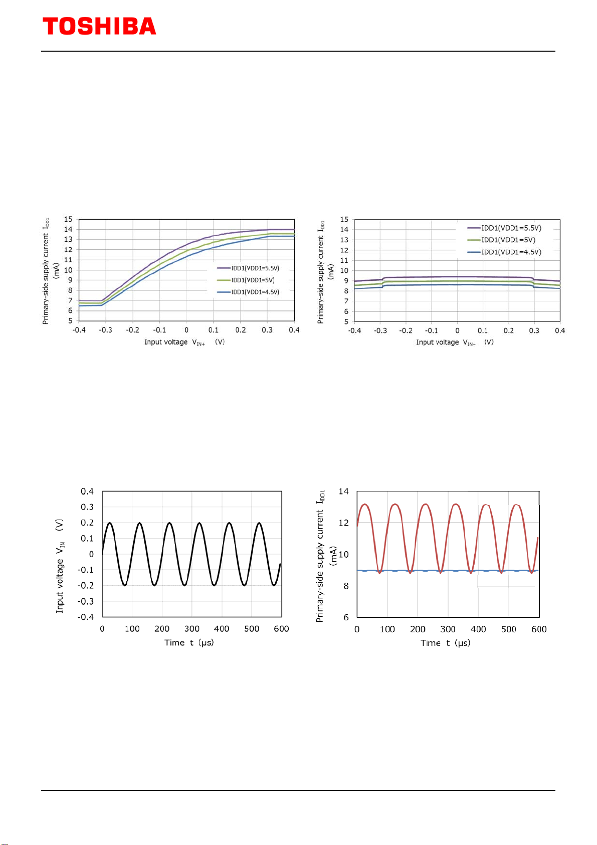
Figure 2. 6 shows the relationships between the input voltage and the primary-side supply
current of the TLP7820 ( B) side) and a competitor’s isolation amplifier ( A) side). The
primary-side supply current of the competitor’s isolation amplifier increases with input voltage
while the TLP7820 has a unique digital encoder/decoder technology to maintain the primary-
side supply current at almost a constant level around 9 mA (typical) over a range of input
voltage (recommend operating range: -0.2 to +0.2 V). This contributes reduction of the
maximum circuit current, simplifying the design of a primary-side power supply.
A) Competitor A B) TLP7820
Figure 2.6 Relationships between the input voltage and the primary-side supply
current of isolation amplifiers
Figure 2.7 (B) shows the changes in the primary-side supply current in response to input
voltage changes at a given frequency in Figure 2.7 (A).
A) Input voltage changes B) Primary-side supply current waveforms
Figure 2.7 Primary-side supply current waveforms in response to input voltage
changes
The primary-side supply current of the competitor’s isolation amplifier changes between 9
mA and 13 mA in response to changes in input voltage while the primary-side supply current
TLP7820
Competitor

RD014-RGUIDE-01
2018-03-15
Rev. 1
9/ 19
© 2018
Toshiba Electronic Devices & Storage Corporation
of the TLP7820 remains around 9 mA regardless of input voltage change. For example, a
floating power supply such as a bootstrap is used as a primary-side power supply for an
isolation amplifier since the floating power supply allows the use of small-value capacitors to
reduce the circuit size. Obviously, the constant supply current of the TLP7820 contributes
power supply consumption reduction and the circuit size reduction. In the trend of increasing
system speed, this also contributes suppress electromagnetic interference (EMI) caused by
large supply voltage fluctuations.
3. Application circuit example and its bill of materials
3.1 Example of an application circuit for voltage sensing
Figure 3.1 shows an example of a voltage-sensing circuit using the TLP7820.
Figure 3.1 Example of a voltage-sensing circuit using the TLP7820

RD014-RGUIDE-01
2018-03-15
Rev. 1
10 / 19
© 2018
Toshiba Electronic Devices & Storage Corporation
3.2 Bill of materials
Table 3.1 shows a bill of materials for the voltage-sensing circuit using the TLP7820
Table 3.1 Bill of materials for the voltage-sensing circuit using the TLP7820
4. Guidelines for designing a voltage-sensing circuit
4.1 Voltage-sensing resistors in a voltage-sensing circuit
For the voltage-sensing purpose, the voltage applied across R1+R2+R3 in Figure 3.1 is detected.
Even if HV is much higher than the input voltage range of an isolation amplifier, it is possible for
TLP7820 to detect divided voltage with a divider. The voltage-sensing error is determined
considering the tolerances of R1, R2, and R3 and the error of the equivalent input resistance Ri (80
kΩ) across Pin 2 and GND of TLP7820. The followings are calculation examples of voltage-sensing
resistors.
Eexample 1:
Sensing error : below 0.5%
Equivalent input resistor of TLP7820 (Ri) : 80 kΩ
R1:R1 // Ri = R1:(R1×80kΩ) / (R1+80kΩ) = 1:0.995
0.995 = 80kΩ/(R1+80kΩ)
0.995 × R1 + 0.995 × 80kΩ = 80 kΩ ∴R1 ≈ 402 Ω
When R1 is selected from E24 series, R1 = 390 Ω.
Applied voltage : 400 V
Detecting voltage : 200 mV
No. Ref. Qty Value Part Number Manufacturer Description Packaging
Typical
Dimensions in
mm (inches)
1 IC1 1 TLP7820 TOSHIBA SO8L 11.05 x 5.85
2 IC2 1 OPA237UA TI SOIC 6.0 x 4.9
3 R1 1 750Ω 0.25 W, ±5% 3216 3.2 x 1.6
(1206)
4 R2 1 750 kΩ 800 V, 0.25 W,
±0.5% 6331 6.3 x 3.1
(2512)
5 R3 1 750 kΩ 800 V, 0.25 W,
±0.5% 6331 6.3 x 3.1
(2512)
6 R4, R5, R6, R7 4 10 kΩ 0.25 W, ±0.5% 2012 2.0 x 1.25
(0805)
7 R8, R9 2 1 kΩ 0.25 W, ±0.5% 2012 2.0 x 1.25
(0805)
8 C1 1 0.5 pF Ceramic, 50 V, ±10% 1005 1.0 x 0.5
(0402)
9 C2, C3, C6 3 100 nF Ceramic, 25V, ±10% 2012 2.0 x 1.25
(0805)
10 C4, C5 2 75 pF Ceramic, 100V, ±5% 1608 1.6 x 0.8
(0603)
11 C7 1 10 μF Ceramic, 16V, ±10% 2012 2.0 x 1.25
(0805)

RD014-RGUIDE-01
2018-03-15
Rev. 1
11 / 19
© 2018
Toshiba Electronic Devices & Storage Corporation
400V:200mV = (R2+R3) + 390Ω:39 Ω
200mV × (R2+R3) + 200mV × 390Ω = 400V × 390Ω
∴R2+R3 ≈ 780 kΩ
When R2 and R3 are selected from E24 series, R2 = 390 Ω and R3 = 390 Ω.
* R2 and R3 are connected in series to ensure creepage distance of resistors.
Eexample 2:
Sensing error : below 1%
Equivalent input resistor of TLP7820 (Ri) : 80 kΩ
R1:R1 // R
i = R1:(R1×80kΩ) / (R1+80kΩ) = 1:0.99
0.99 = 80kΩ/(R1+80kΩ)
0.99 × R1 + 0.99 × 80kΩ = 80 kΩ ∴R1 ≈ 808 Ω
When R1 is selected from E24 series, R1 = 750 Ω.
Applied voltage : 400 V
Detecting voltage : 200 mV
400V:200mV = (R2+R3) + 750Ω:750Ω
200mV × (R2+R3) + 200mV × 750Ω = 400V × 750Ω
∴R2+R3 ≈ 1.5 MΩ
When R2 and R3 are selected from E24 series, R2 = 750 Ω and R3 = 750 Ω.
* R2 and R3 are connected in series to ensure creepage distance of resistors.
The tolerances of R1, R2, and R3 should be considered to calculate actual voltage-sensing error.
4.2 Test mode considerations
The TLP7820 enters test mode when either the VIN+ or VIN- pin exceeds (VDD1-2) volts (e.g., 5V -
2V = 3V when VDD1 = 5V). Don't use the TLP7820 in such a condition.
5. Simulation
5.1 Basic operation
This section shows the simulation results for verifying the basic operation of the TLP7820. Figure
5.1 shows the simulation circuit under the following conditions:
∎ Simulation conditions
· VDD1 of IC1: 5V
· VDD2 of IC1 and V+ of IC2: 3.3V
· Vin
Input voltage (10-kHz sine wave with 0.2Vp-p)

RD014-RGUIDE-01
2018-03-15
Rev. 1
12 / 19
© 2018
Toshiba Electronic Devices & Storage Corporation
Figure 5.1 Simulation circuit to verify basic operation
Figure 5.2 shows the simulation results. The output is a 10kHz sine wave with 1.64Vp-p, which has
x8.2 as large an amplitude as the input signal (10kHz sine wave) with 0.2Vp-p. This is equal to the
specified typical gain of x8.2 of the TLP7820, indicating that simulation ran properly.
Figure 5.2 Simulation results
Vin Vout
Time
0s 50us 100us 150us 200us 250us 300us
1 V(Vin) 2 V(Vout)
-250mV
-200mV
-150mV
-100mV
-50mV
-0mV
50mV
100mV
150mV
200mV
250mV
V
i
n
>> 0.6V
0.8V
1.0V
1.2V
1.4V
1.6V
1.8V
2.0V
2.2V
2.4V
2.6V V
o
u
t
1.64 Vp-p Vout
Vin (Vin1)

RD014-RGUIDE-01
2018-03-15
Rev. 1
13 / 19
© 2018
Toshiba Electronic Devices & Storage Corporation
5.2 Noise superimposed on the input voltage
Running a simulation superimposing a noise signal (a 500-kHz sine wave with 100 mVp-p) on
the input voltage, Vin1. The other conditions are the same as for the previous simulation. Figure
5.3 shows the circuit simulated.
Figure 5.3 Simulation circuit superimposing a noise
Figure 5.4 shows the simulation results, which indicate that the output waveform was not
measured properly due to the influence of the noise.
Figure 5.4 Simulation waveforms with noise
Vin Vout
V_noise is superimposed on Vin1.
Time
0s 50us 100us 150us 200us 250us 300us
1 V(Vin) 2 V(Vout)
-250mV
-200mV
-150mV
-100mV
-50mV
-0mV
50mV
100mV
150mV
200mV
250mV
V
i
n
>> 0.6V
0.8V
1.0V
1.2V
1.4V
1.6V
1.8V
2.0V
2.2V
2.4V
2.6V V
o
u
t
Vout
Vin
1.76 V
p
-
p

RD014-RGUIDE-01
2018-03-15
Rev. 1
14 / 19
© 2018
Toshiba Electronic Devices & Storage Corporation
5.3 Circuit with filters
Running a simulation with input filters. A 100mVp-p noise signal (1MHz sine wave) was
superimposed onto Vin1. The added filters were as follows:
Primary-side input line:
Anti-aliasing LPF frequency: 230kHz
LPF resistor: R1=R2=68Ω
Input bypass capacitor C1 = 0.01μF
Secondary-side output line:
Noise filter frequency: 230kHz
Amplitude adjustment gain: 0 dB
Input series resistors: 10 kΩ
Input bypass capacitors: C4 = C5 =68 pF
Figure 5.5 shows the simulation circuit.
Figure 5.5 Circuit with filters simulated
Figure 5.6 provides the simulation results, which show that the filters removed a noise from the
output waveform. The output is a 10kHz sine wave with 1.64Vp-p, which has x8.2 as large an
amplitude as the input signal (10kHz sine wave) with 0.2Vp-p. This is equal to the specified typical
gain of x8.2 of the TLP7820, indicating that simulation ran properly.
Vin Vout
Filter
Filter

RD014-RGUIDE-01
2018-03-15
Rev. 1
15 / 19
© 2018
Toshiba Electronic Devices & Storage Corporation
Figure 5.6 Results of simulation of a circuit with filters
Time
0s 50us 100us 150us 200us 250us 300us
1 V(Vin) 2 V(Vout)
-250mV
-200mV
-150mV
-100mV
-50mV
-0mV
50mV
100mV
150mV
200mV
250mV
V
i
n
>> 0.6V
0.8V
1.0V
1.2V
1.4V
1.6V
1.8V
2.0V
2.2V
2.4V
2.6V V
o
u
t
1.64 Vp-p Vout
Vin (Vin1+V_noise)

RD014-RGUIDE-01
2018-03-15
Rev. 1
16 / 19
© 2018
Toshiba Electronic Devices & Storage Corporation
6. Product overview
6.1. Overview
The TLP7820 is an optically coupled isolation amplifier that has a high-precision delta-sigma AD
converter at the primary side and a DA converter at the secondary side.
Recommended supply voltage ranges:
Primary side = 4.5 to 5.5 V, Secondary side = 3.0 to 5.5 V
Operating temperature range: -40 to +105°C
Common-mode transient immunity (CMTI): 15kV/μs (minimum)
Low power consumption:
Primary supply current = 8.6 mA (typical), Secondary supply current = 6.2 mA (typical)
Thin package (SO8L) contributes flexible PCB designs
Excellent output nonlinearity characteristics:
NL200=0.02% (typical) at Vin+ = -200mV to +200mV
NL100=0.015% (typical) at Vin+ = -100mV to +100mV
Excellent temperature stability
Input offset drift: 2μV/°C (typical)
Gain drift: 0.00012V/V/°C (typical)
VOUT nonlinearity drift: 0.00007%/°C (typical)
Safety standards
UL-approved: UL1577, File No. E67349
cUL-approved: CSA Component Acceptance Service No. 5A File No. E67349
VDE-approved: EN60747-5-5, EN60065, EN60950-1, EN 62368-1 (Note 1)
CQC-approved: GB4943.1, GB8898
Note 1: When VDE-approved parts are needed, please designate the Option (D4).

RD014-RGUIDE-01
2018-03-15
Rev. 1
17 / 19
© 2018
Toshiba Electronic Devices & Storage Corporation
6.2. External view and pin assignment
Figure 6.1 External view, marking, and pin assignment of the TLP7820
6.3. Internal block diagram
Note: Add 0.1μF bypass capacitors between Pin 1 and Pin 4 and between Pin 5 and
Pin 8.
Figure 6.2 Internal block diagram of the TLP7820
External view and marking
Pin assignment
Pin No. Symbol Description
1V
DD1
Input side supply voltage
2V
IN+
Positive input
3V
IN-
Negative input
4 GND1 Input side ground
5GND2Output side ground
6V
OUT-
Negative output
7V
OUT+
Positive output
8V
DD2
Output side supply voltage

RD014-RGUIDE-01
2018-03-15
Rev. 1
18 / 19
© 2018
Toshiba Electronic Devices & Storage Corporation
6.4 Output voltages for different primary- and secondary-side power supply
combinations
Table 6.1 shows the output voltages obtained from different primary- and secondary-side power
supply combinations.
Table 6.1 Output voltages for different power supply combinations
∎ VOUT+ output ∎ VOUT- output
Primary-Side Power
Supply, VDD1
Primary-Side Power
Supply, VDD1
ON OFF ON OFF
Secondary-
Side Power
Supply
VDD2
ON VIN x Gain/2
+1.25 (V) GND Secondary-
Side Power
Supply
VDD2
ON VIN x Gain/2
+1.25 (V) +2.5 V
OFF GND GND OFF GND GND

RD014-RGUIDE-01
2018-03-15
Rev. 1
19 / 19
© 2018
Toshiba Electronic Devices & Storage Corporation
Terms of Use
This terms of use is made between Toshiba Electronic Devices and Storage Corporation (“We”) and customers who
use documents and data that are consulted to design electronics applications on which our semiconductor devices
are mounted (“this Reference Design”). Customers shall comply with this terms of use. Please note that it is assumed
that customers agree to any and all this terms of use if customers download this Reference Design. We may, at its
sole and exclusive discretion, change, alter, modify, add, and/or remove any part of this terms of use at any time
without any prior notice. We may terminate this terms of use at any time and for any reason. Upon termination of
this terms of use, customers shall destroy this Reference Design. In the event of any breach thereof by customers,
customers shall destroy this Reference Design, and furnish us a written confirmation to prove such destruction.
1. Restrictions on usage
1. This Reference Design is provided solely as reference data for designing electronics applications. Customers shall
not use this Reference Design for any other purpose, including without limitation, verification of reliability.
2. This Reference Design is for customer's own use and not for sale, lease or other transfer.
3. Customers shall not use this Reference Design for evaluation in high or low temperature, high humidity, or high
electromagnetic environments.
4. This Reference Design shall not be used for or incorporated into any products or systems whose manufacture,
use, or sale is prohibited under any applicable laws or regulations.
2. Limitations
1. We reserve the right to make changes to this Reference Design without notice.
2. This Reference Design should be treated as a reference only. We are not responsible for any incorrect or
incomplete data and information.
3. Semiconductor devices can malfunction or fail. When designing electronics applications by referring to this
Reference Design, customers are responsible for complying with safety standards and for providing adequate designs
and safeguards for their hardware, software and systems which minimize risk and avoid situations in which a
malfunction or failure of semiconductor devices could cause loss of human life, bodily injury or damage to property,
including data loss or corruption. Customers must also refer to and comply with the latest versions of all relevant our
information, including without limitation, specifications, data sheets and application notes for semiconductor devices,
as well as the precautions and conditions set forth in the "Semiconductor Reliability Handbook".
4. When designing electronics applications by referring to this Reference Design, customers must evaluate the
whole system adequately. Customers are solely responsible for all aspects of their own product design or applications.
WE ASSUME NO LIABILITY FOR CUSTOMERS' PRODUCT DESIGN OR APPLICATIONS.
5. No responsibility is assumed by us for any infringement of patents or any other intellectual property rights of
third parties that may result from the use of this Reference Design. No license to any intellectual property right is
granted by this terms of use, whether express or implied, by estoppel or otherwise.
6. THIS REFERENCE DESIGN IS PROVIDED "AS IS". WE (a) ASSUME NO LIABILITY WHATSOEVER, INCLUDING
WITHOUT LIMITATION, INDIRECT, CONSEQUENTIAL, SPECIAL, OR INCIDENTAL DAMAGES OR LOSS, INCLUDING
WITHOUT LIMITATION, LOSS OF PROFITS, LOSS OF OPPORTUNITIES, BUSINESS INTERRUPTION AND LOSS OF
DATA, AND (b) DISCLAIM ANY AND ALL EXPRESS OR IMPLIED WARRANTIES AND CONDITIONS RELATED TO THIS
REFERENCE DESIGN, INCLUDING WARRANTIES OR CONDITIONS OF MERCHANTABILITY, FITNESS FOR A
PARTICULAR PURPOSE, ACCURACY OF INFORMATION, OR NONINFRINGEMENT.
3. Export Control
Customers shall not use or otherwise make available this Reference Design for any military purposes, including
without limitation, for the design, development, use, stockpiling or manufacturing of nuclear, chemical, or biological
weapons or missile technology products (mass destruction weapons). This Reference Design may be controlled under
the applicable export laws and regulations including, without limitation, the Japanese Foreign Exchange and Foreign
Trade Law and the U.S. Export Administration Regulations. Export and re-export of this Reference Design are strictly
prohibited except in compliance with all applicable export laws and regulations.
4. Governing Laws
This terms of use shall be governed and construed by laws of Japan.
Table of contents
Other Toshiba Amplifier manuals