Toshiba 28N33B User manual

SERVICE MANUAL
PRINTED IN UK. 2003 C
COLOURTELEVISION
28N33B
TOSHIBA
050-200266
AK37 Chassis

1
CONTENTS
SAFETY PRECAUTIONS: ................................................................................................................................... 2
TV set switched off .......................................................................................................................................... 2
Measu ements ................................................................................................................................................ 2
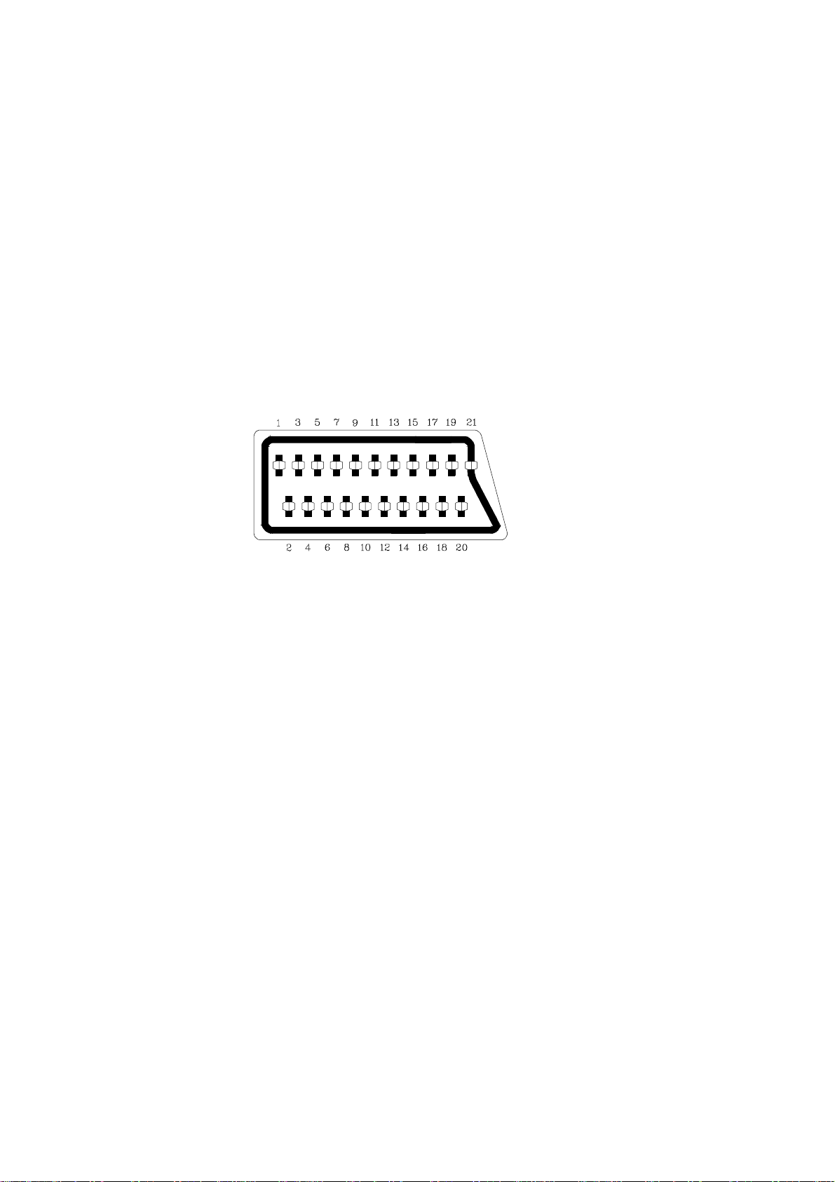
PERI-TV SOCKET ............................................................................................................................................... 2
SCART 1 2
SCART 2 2
1. INTRODUCTION ............................................................................................................................................. 2
2.SMALL SIGNAL PART WITH STV2248 ........................................................................................................... 3
2.1 Vision IF amplifie ................................................................................................................................... 3
2.2 QSS Sound ci cuit (QSS ve sions) ......................................................................................................... 3
2.3 FM demodulato and audio amplifie (mono ve sions) ......................................................................... 3
2.4 Video switch ............................................................................................................................................ 3
2.5 Synch onisation ci cuit ............................................................................................................................ 3
2.6 Ch oma and luminance p ocessing ...................................................................................................... 4
2.7 RGB output ci cuit ................................................................................................................................... 4
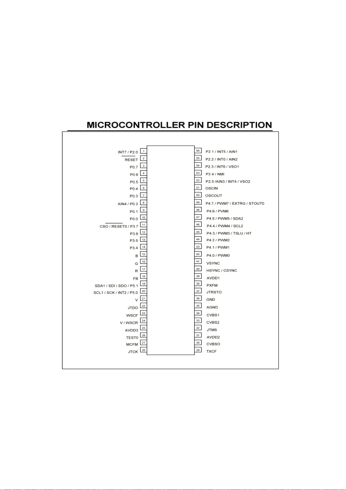
2.8 µ-Cont olle ............................................................................................................................................. 4
3. TUNER ............................................................................................................................................................ 5
4- MULTISTANDARD SOUND PROCESSOR .................................................................................................... 5
5. SOUND OUTPUT STAGE TDA7269A ............................................................................................................. 5
6. VERTICAL OUTPUT STAGE WITH STV9306 ............................................................................................. 5-6
7. VIDEO OUTPUT AMPLIFIER STV5112 ........................................................................................................... 6
8. POWER SUPPLY (SMPS) ............................................................................................................................... 6
9. POWER FACTOR CORRECTION .................................................................................................................. 6
10. SERIAL ACCESS CMOS 8K EEPROM 24C08 ............................................................................................. 6
11. CLASS AB STEREO HEADPHONE DRIVER TDA1308 ................................................................................ 6
12. CLASS AB MONO SUBWOOFER DRIVER TDA7261 ................................................................................... 6
13. SAW FILTERS ............................................................................................................................................... 6
14. IC DESCRIPTIONS AND INTERNAL BLOCK DIAGRAM .............................................................................. 6
ST92195 ....................................................................................................................................................... 7
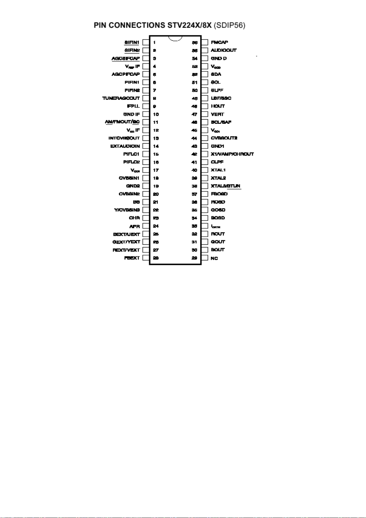
STV224X ................................................................................................................................................... 7-8
UV1315, UV1316, UV1336 ...................................................................................................................... 8-9
TDA7269A .................................................................................................................................................. 10
STV9306 ..................................................................................................................................................... 10
STV5112 ..................................................................................................................................................... 11
MC44608 .................................................................................................................................................... 11
MSP 34XXG ................................................................................................................................................ 12
24C08 ................................................................................................................................................... 12-13
TDA1308 .................................................................................................................................................... 13
TDA7261 .................................................................................................................................................... 13
SAW FILTERS ............................................................................................................................................. 14
15.CIRCUIT DESCCIRIPTION ................................................................................................................... 15-19
16.AK37 CHASSIS MANUAL ADJUSTMENT PROCEDURE ...................................................................... 20-22
17.OPTION SETTING ................................................................................................................................. 23-25
18.TUNER SETTING ........................................................................................................................................ 26
19.GENERAL BLOCK DIAGRAM of CHASSIS 11AK37 .................................................................................... 27
20.AK37 / TITANIUM - Languages G oups ....................................................................................................... 28
21.AK37 PROJECT BLOCK DIAGRAMS .......................................................................................................... 29
21.1 BLOCK DIAGRAM ................................................................................................................................. 30
21.2 SMPS BLOCK DIAGRAM ....................................................................................................................... 31
21.3 MICRO CONTROLLER BLOCK DIAGRAM ........................................................................................... 32
21.4 VIDEO BLOCK DIAGRAM ...................................................................................................................... 33
21.5 STEREO BLOCK DIAGRAM .................................................................................................................. 34
21.6 SCART BLOCK DIAGRAM ..................................................................................................................... 35
21.7 DEFLECTIOAN BLOCK DIAGRAM ........................................................................................................ 36
21.8 BASE BOADR BLOCK DIAGRAM .......................................................................................................... 37
22. CIRCUIT DIAGRAMS .................................................................................................................................. 38
22.1 SMPS CIRCUIT DIAGRAM .................................................................................................................... 38
22.2 MICRO CONTROLLER CIRCUIT DIAGRAM ......................................................................................... 39
22.3 VIDEO CIRCUIT DIAGRAM ................................................................................................................... 40
22.4 STEREO CIRCUIT DIAGRAM ............................................................................................................... 41
22.5 SCART CIRCUIT DIAGRAM .................................................................................................................. 42
22.6 BASE BOARD CIRCUIT DIAGRAM ....................................................................................................... 43
22.7 CRT BOARD CIRCUIT DIAGRAM ......................................................................................................... 44

2
DO NOT CHANGE ANY MODULE UNLESS THE SET IS SWITCH OFF
The mains supply side of the switch mode power supply transformer is live.
Use an isolating transformer.
The receivers fulfill completely the safety requirements.
Safety precautions
Servicing of this TV should only be carried out by a qualified person. Components marked with the warning symbol
on the circuit diagram are critical for safety and must only be replaced with an identical component.
- ower resistor and fusable resistors must be mounted in an identical manner to the original component.
TV Set switched off
Make short-circuit between HV-CRT clip and CRT ground layer.
Short C809 before changing IC800 end IC801 or other components in primary side of SM S part.
Measurements
Voltage readings and oscilloscope traces are measured under following conditions.
Antenna signals level is 60dB at the color bar pattern from the TV pattern generator.(100% white,75% colour saturation)
Brightness, contrast, and color are adjusted for normal picture perfomance.
Mains supply, 220VAC, 50Hz.
PERI-TV SOCKET
SCART 1 PINING SCART 2 PINING
1 Audio right output 0.5Vrms / 1K 1 Audio right output 0.5Vrms / 1K
2 Audio right input 0.5Vrms / 10K 2 Audio right input 0.5Vrms / 10K
3 Audio left output 0.5Vrms / 1K 3 Audio left output 0.5Vrms / 1K
4 Ground AF 4 Ground AF
5 Ground Blue 5 Ground Blue
6 Audio left input 0.5Vrms / 10K 6 Audio left input 0.5Vrms / 10K
7 Blue input 0.7Vpp / 75ohm 7 Blue input
8 AV switching input 0-12VDC /10K 8 AV switching input 0-12VDC /10K
9 Ground Green 9 Ground Green
10 - 10 -
11 Green input 0.7Vpp / 75ohm 11 -
12 - 12 -
13 Ground Red 13 Ground Red
14 Ground Blanking 14 Ground Blanking
15 Red input 0.7Vpp / 75ohm 15 -
16 Blanking input 0-0.4VDC, 1-3VDC / 75ohm 16 -
17 Ground CVBS output 17 Ground CVBS output
18 Ground CVBS input 18 Ground CVBS input
19 CVBS output 1Vpp / 75ohm 19 CVBS output 1Vpp / 75ohm
20 CVBS input 1Vpp / 75ohm 20 CVBS input 1Vpp / 75ohm
21 Ground 21 Ground
1. INTRODUCTION
11AK37 is a 110° chassis capable of driving 25, 28, 29, 33 4:3 and 28, 32 16:9 tubes at the appropriate currents.
The chassis is capable of operating in AL, SECAM and NTSC standards and multiple transmission standards as B/G,
D/K, I/I, and L/L´. standards. The sound system is capable of giving 12 watts RMS output into a load of 8 ohms.
One page, 7 page SIM LETEXT, TO TEXT, FASTTEXT and US Closed Caption is also provided. The chassis is
equipped with a double-deck 42 pin scart connector for AV input/output, front-AV input, one back-AV output, one SVHS,
one headphone and one subwoofer.

3
2. SMALL SIGNAL PART WITH STV2248:
STV2248 video processor is essential for realizing all small signal functions for a color TV receiver.
2.1 Vision IF amplifier
The vision IF amplifier can demodulate signals with positive and negative modulation. The LL demodulator is
completely alignment-free. Although the VCO (Toko-coil) of the LL circuit is external, yet the frequency is fixed to the
required value by the original manufacturer thus the Toko-coil does not need to be adjusted manually. The setting of the
various frequencies (38.9 or 45.75 MHz) can be made via changing the coil itself
2.2 QSS Sound circuit (QSS versions)
The sound IF amplifier is similar to the vision IF amplifier and has an external AGC de-coupling capacitor. The single
reference QSS mixer is realised by a multiplier. In this multiplier the SIF signal is converted to the inter-carrier frequency
by mixing it with the regenerated picture carrier from the VCO. The mixer output signal is supplied to the output via a
high-pass filter for attenuation of the residual video signals. With this system a high performance hi-fi stereo sound
processing can be achieved. The AM sound demodulator is realised by a multiplier. The modulated sound IF signal is
multiplied in phase with the limited SIF signal. The demodulator output signal is supplied to the output via a low-pass
filter for attenuation of the carrier harmonics. The AM signal is supplied to the output via the volume control.
The AM demodulated signal results from multiplying the input signal by itself, it is available on AM/FM output.
2.3 FM demodulator and audio amplifier (mono versions)
The FM demodulator is realized as narrow-band LL with external loop filter, which provides the necessary selectivity
without using an external band-pass filter. To obtain a good selectivity a linear phase detector and constant input signal
amplitude are required. For this reason the inter-carrier signal is internally supplied to the demodulator via a gain
controlled amplifier and AGC circuit. The nominal frequency of the demodulator is tuned to the required frequency
(4.5/5.5/6.0/6.5 MHz) by means of a calibration circuit that uses the clock frequency of the µ-controller/Teletext decoder
as a reference. The setting to the wanted frequency is realized by means of the software. It can be read whether the LL
frequency is inside or outside the window and whether the LL is in lock or not. With this information it is possible to
make an automatic search system for the incoming sound frequency. This is realized by means of a software loop that
alternate the demodulator to various frequencies, then select the frequency on which a lock condition has been found.
De-emphasis output signal amplitude is independent of the TV standard and has the same value for a frequency deviation
of ±25 kHz at the 4.5 MHz standard and for a deviation of ±50 kHz for the other standards. When the IF circuit is
switched to positive modulation the internal signal on de-emphasis pin is automatically muted. The audio control circuit
contains an audio switch and volume control. In the mono inter-carrier sound versions the Automatic Volume Leveling
(AVL) function can be activated. The pin to which the external capacitor has to be connected depends on the IC version.
2.4 Video switching
The video processor (STV2248C) has three CVBS inputs and two RGB inputs. The first CVBS input is used for external
CVBS from SCART 1, the second is used for either CVBS or Y/C from either SCART2 or BAV/FAV or SVHS, and the
third one is used for internal video. The selection between both external video inputs signals is realized by means of
software and hardware switches.
2.5 Synchronization circuit
The video processor (STV224X) performs the horizontal and vertical processing. The external horizontal deflection circuit
is controlled via the Horizontal output pulse (HOUT). The vertical scanning is performed through an external ramp
generator and a vertical power amplifier IC controlled by the Vertical output pulse (VOUT).
The main components of the deflection circuit are:
LL1: the first phase locked loop that locks the internal line frequency reference on the
CVBS input signal. It is composed of an integrated VCO (12 MHz) that requires the chroma reference frequency
(4.43MHz or 3.58MHz crystal oscillator reference signal), a divider by 768, a line decoder, and a phase comparator.
LL2: The second phase locked loop that controls the phase of the horizontal output
(Compensation of horizontal deflection transistor storage time variation). Also the horizontal position adjustment is
also performed in LL2.
A vertical pulse extractor.
A vertical countdown system to generate all vertical windows (vertical synchronization window, frame blanking pulses,
50/60Hz identification window...).
Automatic identification of 50/60Hz scanning.
LL1 time constant control.
Noise detector, video identification circuits, and horizontal coincidence detector.
Vertical output stage including de-interlace function, vertical position control.
Vertical amplitude control voltage output (combined with chroma reference output and Xtal 1 indication).

4
2.6 Chroma and luminance processing
The chroma decoder is able to demodulate AL, NTSC and SECAM signals.
The decoder dedicated to AL and NTSC sub-carrier is based on a synchronous demodulator, and an Xtal LL locked on
the phase reference signal (burst).
The SECAM demodulation is based on a LL with automatic calibration loop.
The color standard identification is based on the burst recognition.
Automatic and forced modes can be selected through the I 2C bus.
NTSC tint, and auto flesh are controlled through I 2C bus.
Xtal LL can handle up to 3 crystals to work in AL M, AL N and NTSC M for South America.
ACC an ACC overload control the chroma sub-carrier amplitude within 26dB range. Both
ACC s are based on digital systems and do not need external capacitor.
All chroma filters are fully integrated and tuned via a LL locked on Xtal VCO signal.
A second LL is used for accurate fine-tuning of the SECAM bell filter. This tuning is achieved during the frame blanking.
An external capacitor memorizes the bell filter tuning voltage.
A base-band chroma delay-line rebuilds the missing color line in SECAM and removes transmission phase errors in AL.
The base-band chroma delay line is clocked with 6MHz signal provided by the horizontal scanning VCO.
The luminance processor is composed of a chroma trap filter, a luminance delay line, a peaking function with noise
coring feature, a black stretch circuit.
Trap filter and luminance delay lines are achieved with the use of bi-quad integrated filters, auto-aligned via a master
filter phase locked loop.
2.7 RGB output circuit
The video processor performs the R, G, B processing.
There are three sources:
1. Y,U,V inputs (coming from luma part (Y output), and chroma decoder outputs (R-Y, B-Y outputs).
2. External R,G,B inputs from SCART (converted internally in Y,U,V), with also the possibility to input YUV signals from
a DVD player, (YUV specification is Y=0.7 V , U= 0.7 V , V = 0.7V for 100% color bar).
3. Internal R,G,B inputs (for OSD and Teletext display)
The main functions of the video part are:
Y,U,V inputs with integrated clamp loop, allowing a DC link with YUV outputs,
External RGB inputs (RGB to YUV conversion), or direct YUV inputs,
Y,U,V switches,
Contrast, saturation, brightness controls,
YUV to RGB matrix,
OSD RGB input stages (with contrast control),
RGB switches,
A R function,
DC adjustment of red and green channels,
Drive adjustments (R, G, B gain),
Digital automatic cut-off loop control,
Manual cut-off capability with I 2C adjustments,
Half tone, oversize blanking, external insertion detection, blue screen,
Blanking control and RGB output stages.
2.8 µ-Controller
The ST92195 is the micro-controller, which is required for a color TV receiver. ST92195D1 is the version with one page
Teletext and ST92195D7 is the one with 7 page Teletext. The IC has the supply voltages of 5 V and they are mounted in
SDI package with 56 pins.
µ-Controller has the following features
Display of the program number, channel number, TV Standard, analogue values, sleep timer, parental control and mute
is done by OSD
Single LED for standby and on mode indication
System configuration with service mode
3 level logic output for SECAM and Tuner band switching

5
3. TUNER
Either a LL or a VST tuner is used as a tuner.
UV1316 (VHF/UHF) is used as a LL tuner. For only AL M/N, NTSC M applications UV 1336 is used as the LL tuner.
UV 1315 (VHF/UHF) is used as a VST Tuner.
Channel coverage of UV1316
%$1'
2))$,5&+$11(/6 &$%/(&+$11(/6
&+$11(/6&+$11(/6
/RZ%DQG(WR&WR6WR6WR
0LG%DQG(WR(WR6WR6WR
+LJK%DQG(WR(WR6WR6WR
)5(48(1&<
5$1*(0+] )5(48(1&<
5$1*(0+]
(1). Enough margin is available to tune down to 45.25 MHz.
(2). Enough margin is available to tune up to 863.25 MHz.
Noise Typical Max. Gain Min. Typical Max.
Low band : 5dB 9dB All channels : 38dB 44dB 52dB
Mid band : 5dB 9dB Gain Taper (of-air channels) : 8dB
High band : 6dB 9dB
Channel Coverage UV1336
%$1'
&+$11(/6
/RZ%DQGWR'WR
0LG%DQG(WR33WR
+LJK%DQG444WRWR
)5(48(1&<
5$1*(0+]
Noise is typically 6dB for all channels. Gain is minimum 38dB and maximum 50dB for all channels.
Channel Coverage of UV1315
%$1'
2))$,5&+$11(/6 &$%/(&+$11(/6
&+$11(/6&+$11(/6
/RZ
%DQG
(
WR
&
WR
6
WR
6
WR
0LG%DQG(WR(WR6WR6WR
+LJK%DQG(WR(WR6WR6WR
)5(48(1&<
5$1*(0+] )5(48(1&<
5$1*(0+]
(1). Enough margin is available to tune down to 45.25 MHz.
(2). Enough margin is available to tune up to 863.25 MHz.
Noise Typ. Max. Gain Min. Typ. Max.
Low band : 6dB 9dB All Channels : 38dB 44dB 50dB
Mid band : 6dB 10dB Gain Taper : 8dB
High band : 6dB 11dB (off-air channels)
4. MULTISTANDARD SOUND PROCESSOR
The MS 34xxG is designed to perform demodulation of FM or AM-Mono TV sound. Three kinds of MS s are used:
MS 3400G,MS 3410G and MS 3411G. The MS 3400G is fully pin and software-compatible to the MS 3410G,
but is not able to decode NICAM. It is also compatible to the MS 3411G,sound processor IC with virtual dolby sound.
5. SOUND OUTPUT STAGETDA7269A
The TDA7269A is a class AB dual Audio power amplifier, specially designed for high quality sound applications as
Hi-Fi music centers and TV sets. It is supplied by ±12VDC coming from two separate windings in the SM S transformer.
It gives 2x14W(THD=10%) output power into an 8ohm load.
6. VERTICAL OUTPUT STAGE WITH STV9306
The STV9306 is a fully I2C controlled vertical deflection IC designed for use in 110°, 4/3 or 16/9 CRT applications.
It integrates both the vertical deflection and E/W correction circuitries necessary in design of a 110° chassis.

6
7. VIDEO OUTPUT AMPLI IER STV5112
The STV5112 consists of three monolithic video output amplifiers. The amplifier can be seen as an operational
amplifier with negative feedback. The advantage of negative feedback is that the amplifier characteristics do not play
an important role up to certain frequencies. The internal flash diodes protect the amplifiers against flash over in the
picture tube. The only protections required at the cathode outputs are a flash resistor and a spark gap.
Furthermore, the device has a high voltage power supply (VDD) and a low voltage one (VCC).
8. POWER SUPPLY (SMPS)
The DC voltages required at various parts of the chassis are provided by an SM S transformer controlled by the
IC MC44608 which is designed for driving, controlling and protecting switching transistor of SM S. The transformer
produces 150V for FBT input, ±12V for audio output IC, +5V and +8V for ST92195.
9. POWER ACTOR CORRECTION
assive components are used for the solution of power factor correction.
10. SERIAL ACCESS CMOS 8K EEPROM 24C08
The 24C08 is a 8Kbit electrically erasable programmable memory (EE ROM), organized as 4 blocks of 256*08 bits.
The memory is compatible with the I²C standard, two wire serial interface which uses a bi-directional data bus and serial
clock.
11. CLASS AB STEREO HEADPHONE DRIVER TDA1308
The TDA1308 is an integrated class AB stereo headphone driver contained in a DI 8 plastic package.
12. CLASS AB MONO SUBWOO ER DRIVER TDA7261
The TDA7261 is a class AB dual Audio power amplifier, specially designed for high quality sound applications in mono
TV chassis. It is supplied by ±12VDC.
13. SAW ILTERS
Saw filter type Model
G1975M AL B/G MONO
K2966M AL SECAM B/G/D/K/I MONO
J1981 AL-I MONO
K2958M AL-SECAM B/G-D/K (38) MONO
K2962M AL-SECAM B/G/D/K/I/L/L MONO
L9653M SECAM L/L AM MONO (AUDIO IF)
G3967M AL-SECAM B/G STEREO (VIDEO IF)
G9353M AL-SECAM B/G STEREO (AUDIO IF)
K3958M AL-SECAM B/G/D/K/I/L/L STEREO (VIDEO IF)
K9356M AL-SECAM B/G/D/K/I STEREO (AUDIO IF)
K9656M AL-SECAM B/G/D/K/I/L/L STEREO (AUDIO IF)
K3958M AL I NICAM (VIDEO IF)
K9356M AL I NICAM (AUDIO IF)
M1962M AL M/N NTSC M MONO
M3953M AL M/N NTSC M STEREO (VIDEO IF)
M9370M AL M/N NTSC M STEREO (AUDIO IF)
IC DESCRIPTIONS AND INTERNAL BLOCK DIAGRAM
ST92195
STV224X
TUNER (UV1315, UV1316, UV1336)
TDA7269A
STV9306
STV5112
MC44608
MS 34XXG
24C08
TDA1308
SAW FILTERS
G1975M, K2966M, K2962M, L9653M, G3962M, G9353M, K3958M, K9356M, K9656M, K6263K, K9652M,
M1962M, M3953M, M9370M

7
ST92195
The ST92195 is a member of the ST9+ family of micro-controllers, completely developed and produced by
SGS-THOMSON Microelectronics using a proprietary n-well HCMOS process. The nucleus of the ST92195 is the
advanced Core, which includes the Central rocessing Unit (C U), the ALU, the Register File and the interrupt controller.
The Core has independent memory and register buses to add to the efficiency of the code. A set of on-chip peripherals
form a complete sys-tem for TV set and VCR applications:
Voltage Synthesis
V S/WSS Slicer
Teletext Slicer
Teletext Display RAM
OSD
Additional peripherals include a watchdog timer, a serial peripheral interface (S I), a 16-bit timer and an A/D converter.
STV224X Video processor:
The STV2246/2247/2248 are fully bus controlled ICs for TV including IF, SIF, luma, chroma and deflection processing.
Used with a vertical frame booster (TDA1771 or TDA8174 for 90° chassis, STV9306 for 110° chassis), they allow the
design of multi-standard (BGDKIMNLL, AL/ SECAM/NTSC) sets with very few external components and no manual
adjustments.

8
UV1315, UV1316, UV1336
General description of UV1315
The UV1315 tuner belongs to the UV 1300 family of tuners, which are designed to meet a wide range of applications.
It is a combined VHF, UHF tuner suitable for CCIR systems B/G, H, L, L, I and I.
Features of UV1315
Member of the UV1300 family small sized UHF/VHF tuners
Systems CCIR:B/G, H, L, L, I and I; OIRT:D/K
Voltage synthesized tuning (VST)
Off-air channels, S-cable channels and Hyper-band
Standardized mechanical dimensions and pinning
PINNING PIN VALUE
1. Gain control voltage (AGC) : 4.0V, Max:4.5V
2. Tuning voltage
3. High band switch : 5V, Min:4.75V, Max:5.5V
4. Mid band switch : 5V, Min:4.75V, Max:5.5V
5. Low band switch : 5V, Min:4.75V, Max:5.5V
6. Supply voltage : 5V, Min:4.75V, Max:5.5V
7. Not connected
8. Not connected
9. Not connected
10. Symmetrical IF output 1
11. Symmetrical IF output 2

9
Band switching table:
+,*+%$1' 9
9
9
0,'%$1' 9 9
99
/2:%$1' 9 9
3,1 3,1 3,1
General description of UV1316
The UV1316 tuner belongs to the UV 1300 family of tuners, which are designed to meet a wide range of applications.
It is a combined VHF, UHF tuner suitable for CCIR systems B/G, H, L, L, I and I.
Features of UV1316
Member of the UV1300 family small sized UHF/VHF tuners
Systems CCIR: B/G, H, L, L, I and I; OIRT: D/K
Digitally controlled ( LL) tuning via I²C-bus
Off-air channels, S-cable channels and Hyper-band
World standardized mechanical dimensions and world standard pinning
Complies to CENELEC EN55020 and EN55013
PINNING PIN VALUE
1. Gain control voltage (AGC) : 4.0V, Max:4.5V
2. Tuning voltage
3. I²C-bus address select : Max:5.5V
4. I²C-bus serial clock : Min:-0.3V, Max:5.5V
5. I²C-bus serial data : Min:-0.3V, Max:5.5V
6. Not connected
7. LL supply voltage : 5.0V, Min:4.75V, Max:5.5V
8. ADC input
9. Tuner supply voltage : 33V, Min:30V, Max:35V
10.Symmetrical IF output 1
11.Symmetrical IF output 2
General description of UV1336
UV1336 series is developed for reception of channels broadcast in accordance with the M, N standard.
Features of UV1336
Global standard pinning
Integrated Mixer-Oscillator & LL function
Conforms to CIS R 13, FCC and DOC (Canada) regulations
Low power consumption
Both phono connector and F connector are available
PINNING PIN VALUE
1. Gain control voltage : 4.0V, Max:4.5V
2. Tuning voltage
3. Address select : Max:5.5V
4. Serial clock : Min:-0.3V, Max:5.5V
5. Serial data : Min:-0.3V, Max:5.5V
6. Not connected
7. Supply voltage : 5.0V, Min:4.75V, Max:5.5V
8. ADC input (optional)
9. Tuning supply voltage : 33V, Min:30V, Max:35V
10.Ground
11. IF output

10
TDA7269A
General Description of TDA7269A
The TDA7269A is a class AB dual Audio power amplifier, specially designed for high quality sound applications as
Hi-Fi music centers and TV sets. Requires very few external components.
Wide supply voltage range up to ±20V
Split supply
High output power; 14 + 14W @THD =10%, RL =8W,VS= ±16V
No pop at turn-on/off
Mute ( op free)
Stand-by feature
Thermal overload protection
Short circuit protection to gnd
PINNING
1. - VS
2. Output1
3. + VS
4. Output2
5. Mute
6. - VS
7. In+(2)
8. In-(2)
9. Gnd
10. In-(1)
11. In+(1)
STV9306
General description
The STV9306 is a fully I2C controlled vertical deflection IC designed for use in 110°, 4/3 or 16/9 CRT applications.
It integrates both the vertical deflection and E/W correction circuitries necessary in design of a 110° chassis.
FEATURES
FULLY I2C CONTROLLED
DMOS OWER HALF-BRIDGE AM LIFIER
DC COU LED O ERATION
INTERNAL FLYBACK GENERATOR (U TO 60V)
SELF ADA TED SAWTOOTH (50/60Hz)
100Hz O ERATION
VERTICAL LINEARITY, AM LITUDE AND CENTERING ADJUSTMENTS
HORIZONTAL WIDTH, INCUSHION, TRA EZOID AND CORNER ADJUSTMENTS
BREATHING CORRECTION
4/3, 16/9 CRT A LICATION
THERMAL ROTECTION
LINEAR VERTICAL ZOOM FUNCTION
E/W CLASS A OUT UT
LOW EXTERNAL COM ONENTS
PINNING
1. SCL
2. CRAM
3. SDA
4. CHOLD
5. SYNC
6. Vs
7. FLYBACK
8. GND
9. OUT
10. VO S
11. EWOUT
12. SENS2
13. EWFB
14. SENS1
15. BREATHING

11
STV5112
General Description
The STV5112 includes three video amplifiers designed with a high voltage bipolar/CMOS/DMOS technology (BCD).
It drives directly the three cathodes and is protected against flashovers. Thanks to its three cathode current outputs,
the STV5112 can be used with both parallel and sequential sampling applications.
Bandwidth : 8MHz TY ICAL
Supply Voltage : 220V typical
Rise and fall time : 50ns typical
CRT cathode current outputs for parallel or sequential cut-off or drive adjustment
Flashover protection
ower dissipation : 3.6W
PINNING PIN VALUE
1. BLUE IN UT
2. VCC LOW VOLTAGE
3. GREEN IN UT
4. RED IN UT
5. VDD HIGH VOLTAGE
6. RED CATHODE CURRENT
7. RED OUT UT
8. GROUND
9. RED FEEDBACK
10. GREEN OUT UT
11. GREEN CATHODE CURRENT
12. GREEN FEEDBACK
13. BLUE OUT UT
14. BLUE CATHODE
15. BLUE FEEDBACK
MC44608
General description
The MC44608 is a high performance voltage-mode controller designed for offline converters. This high voltage
circuit that integrates the startup current source and the oscillator capacitor, requires few external components while
offering a high flexibility and reliability.The device also features a very high efficiency standby management consisting
of an effective ulsed Mode operation. This technique enables the reduction of the standby power consumption to
approximately 1W while delivering 300mW in a 150W SM S.
Integrated startup current source
Loss less offline startup
Direct offline operation
Fast startup
General Features
Flexibility
Duty cycle control
On chip oscillator switching frequency 40, or 75kHz
Secondary control with few external components
Protections
Maximum duty cycle limitation
Cycle by cycle current limitation
Demagnetization (Zero current detection) protection
Over VCC protection against open loop
rogrammable low inertia over voltage protection against open loop
Internal thermal protection
GreenLine Controller
ulsed mode techniques for a very high efficiency low power mode
Lossless startup
Low dV/dT for low EMI radiations
PINNING PIN VALUE
1. Demagnetization Zero cross detection voltage: 50-mV typ.
2. I Sense Over current protection voltage 1V typ.
3. Control Input Min: 7.5V Max.: 18V
4. Ground Iout 2Ap-p during scan 1.2Ap-p during flyback
5. Driver Output resistor 8.5 Ohm sink 15 Ohm source typ.
6. Supply voltage Max:16V (Operating range 6.6V-13V)
7. No connection
8. Line Voltage Min:50V Max:500V

12
MSP 34XXG
General description
The MS 34xxG family of single-chip Multi-standard Sound rocessors covers the sound processing of all analog
TV standards worldwide, as well as the NICAM digital sound standards. The full TV sound processing, starting with
analog sound IF signal-in, down to processed analog AF-out, is performed on a single chip.
Two-carrier FM systems according to the German or Korean terrestrial specs or the satellite specs can be processed
with the MS 34x0G. Digital demodulation and decoding of NICAM-coded TV stereo sound, is done only by the
MS 3410G. The MS 34x0G offers a powerful feature to calculate the carrier field strength, which can be used for
automatic standard detection (terrestrial) and search algorithms (satellite).
The MS 3411G has all functions of the MS 34x0G with the addition of a virtual surround sound feature. Surround
sound can be reproduced to a certain extent with two loudspeakers. The MS 3411G includes our virtualizer algorithm
3D- ANORAMA which has been approved by the Dolby Laboratories for compliance with the Virtual Dolby Surround
technology. In addition, the MS 34x1G includes our ANORAMA algorithm. The MS 34x1G has built-in automatic
functions: The IC is able to detect the actual sound standard automatically (Automatic Standard Detection).
Furthermore, pilot levels and identification signals can be evaluated internally with subsequent switching between
mono/ stereo/ bilingual; no I 2C interaction is necessary (Automatic Sound Selection).
General Features
Two selectable analog inputs (TV and SAT-IF sources)
Automatic Gain Control (AGC) for analog IF input. Input range: 0.103 V pp
Integrated A/D converter for sound-IF inputs
All demodulation and filtering is performed on chip and is individually programmable
Easy realization of all digital NICAM standards (B/G, D/K, I & L) with MS 3410G.
FM demodulation of all terrestrial standards (incl. identification decoding)
FM demodulation of all satellite standards
No external filter hardware is required
Only one crystal clock (18.432 MHz) is necessary
FM carrier level calculation for automatic search algorithms and carrier mute function
Subwoofer output with on-chip programmable low-pass and complementary high-pass filters
DSP Section (Audio Base band Processing)
Flexible selection of audio sources to be processed
Two digital input and one output interface via I 2 S bus for external DS processors, featuring surround sound, ADR etc.
Digital interface to process ADR (ASTRA Digital Radio) together with DR 3510A
erformance of all de-emphasis systems including adaptive Wegener anda1 without external components or controlling
Digitally performed FM identification decoding and de-matrixing
Digital base-band processing: volume, bass, treble, 5-band equalizer, loudness, pseudo-stereo, and base-width enlargement
· Simple controlling of volume, bass, treble, equalizer etc.
Analog Section
four selectable analog pairs of audio base-band inputs (= four SCART inputs) input level: =<2 V RMS,
input impedance: >=25 kW
one analog mono input (i.e. AM sound): input level: =<2 V RMS , input impedance: >=15 kW
two high-quality A/D converters, S/N-Ratio: >=85 dB
20 Hz to 20 kHz bandwidth for SCART-to-SCART copy facilities
24CO8
General description
The 24C16 is a 8Kbit electrically erasable programmable memory (EE ROM), organized as 4 blocks of 256 * 08 bits.
The memory operates with a power supply value as low as 2.5V.
Features
Minimum 1 million ERASE/WRITE cycles with over 10 years data retention
Single supply voltage:4.5 to 5.5V
Two wire serial interface, fully I²C-bus compatible
Byte and Multi-byte write (up to 8 bytes)
age write (up to 16 bytes)
Byte, random and sequential read modes
Self timed programming cycle

13
PINNING PIN VALUE
1. Write protect enable : 0V
2. Not connected : 0V
3. Chip enable input : 0V
4. Ground : 0V
5. Serial data address input/output : Input LOW voltage : Min : -0.3V, Max : 0.3*Vcc
: Input HIGH voltage : Min : 0.7*Vcc, Max : Vcc+1
6. Serial clock : Input LOW voltage : Min : -0.3V, Max : 0.3*Vcc
: Input HIGH voltage : Min : 0.7*Vcc, Max : Vcc+1
7. Multibyte/ age write mode : Input LOW voltage : Min : -0.3V, Max : 0.5V
: Input HIGH voltage : Min : Vcc-0.5, Max : Vcc+1
8. Supply voltage : Min : 2.5V, Max : 5.5V
TDA1308
Features
Wide temperature range
Excellent power supply ripple rejection
Low power consumption
Short-circuit resistant
High performance
high signal-to-noise ratio
low distortion
PINNING PIN VALUE
1. Output A (Voltage swing) : Min:0.75V, Max:4.25V
2. Inverting input A : Vo(clip):Min:1400mVrms
3. Non-inverting input A : 2.5V
4. Ground : 0V
5. Non-inverting input B : 2.5V
6. Inverting input B : Vo(clip):Min:1400mVrms
7. Output B (Voltage swing) : Min:0.75V, Max:4.25V
8. ositive supply : 5V, Min:3.0V, Max:7.0V
TDA7261
General Description of TDA7261
The TDA7261 is a class AB dual Audio power amplifier, specially designed for high quality sound applications in
mono TV sets.
Wide supply voltage range up to 50V ABS max.
Split supply
High output power;25W @THD =10%, RL =8W,VS= ±20V
No pop at turn-on/off
Mute ( op free)
Stand-by feature
Thermal overload protection
Short circuit protection to gnd
PINNING
1. N.C.
2. + VS
3. Output
4. Mute/Stby
5. - VS
6. In
7. GND
8. N.C.

14
Saw filters list:
0
2
1
2
36%*'..
,,
36%*'..
//
.0
.0/
3$/,, -
36%*'. .0
3$/%* *0
9,'(2 $8',2
6
7
5
36%*'..// .0.
36%*'..,, .0.
3$/,, .0.
3$/%* *0*0
9,'(2 $8',2
PINNING
1. Input
2. Input-ground
3. Chip carrier-ground
4. Output
5. Output
K9656M, L9653M
PINNING
1. Input
2. Switching Input
3. Chip carrier-ground
4. Output
5. Output

15
CIRCUIT DESCIRIPTION
POWER SUPPLY
The ZX series of receivers incorporate a Motorola switch mode power supply using a MC 44608-regulator controller IC.
The circuit provides power to the receiver in both standby and normal operation modes.
START UP
The switch on the mains supply is fed through the mains filter network TR801, the surge limiter resistor R831, the bridge
rectifier D891, and reservoir capacitor C809 producing approx. 320 volts D.C to feed the switching MOSFET Q801 via
the primary winding of TR802 pins 6 and 8.
Start up resistor R801 feeds from a 500V coming from the mains through the adder diode D809 to pin 8 of IC800, the IC
uses 9mA current source and connects it internally to VCC at pin6 allowing a rapid charge enough for start up.
Then IC800 responds with the oscillator starting to oscillate at a 40khz frequency fixed by the IC manufacturer.
The IC then produces, pulse width modulation pulses, at this frequency on pin 5 to drive the base of the switching
FET Q801, that will then switch current on and off through the primary of TR802, which will in turn provides voltages in the
secondary windings. The secondary winding voltages being proportional to the length of time that Q801 is turned on in
each cycle. The voltage produced between pins 4 and 3 of TR802 is rectified by D804 developing approx. 12 volts on C810,
which takes over from the start up resistor to supply pin 8 of IC800.
The Demag pin at pin1 offers 3 different functions: Zero voltage crossing detection (50mV), 24mA current detection and
120mA current detection. The 24mA level is used to detect the secondary reconfiguration status and the 120mA level to
detect an Over Voltage status called Quick OV . The VCC at pin6 operates between 6,6V and 13V in normal operation,
when this voltage exceeds 15V then the IC output is disabled.
VOLTAGE REGULATION
After initial start up the secondary voltages of TR802 are established. These voltages then need to be regulated to the
required levels. In a switch mode power supply such as this, it is the ON time of the switching FET Q801 that determines
the output voltages produced. To provide regulation of the supply there is a feedback loop via an adjustable zener IC818
and an O TO- coupler connected to pin3 of IC800. The reference voltage of IC818 is set to 2,5V to supply a B+ voltage of
150V. Any fluctuation at this pin will cause IC800 to compensate it either by increasing or decreasing the voltage at the
secondary outputs.
VOLTAGE PROTECTION
The MC44608 offers two OV functions:
1- A fixed function that detects when V CC is higher than 15.4V
2- A programmable function that uses the demag pin. The current flowing into the demag pin is mirrored and compared
to the reference current Iovp (120mA). -Thus this OV is quicker than normal number one as it directly sense the change
in current rather than waiting for a specific voltage value, and is called QOV . In both cases, once an OV condition is
detected, the output is latched off until a new circuit STARTU .
3- A software controlled function acts on pin52 of IC501. This pin monitors feedback from both 8V and 5V via D512, then
compares these to a reference value Vref pre-set by the hardware through resistors R545, R546, R548. In normal mode
operation 1.2V < Vref < 2.2V. Any voltage outside this window will cause the micro controller to force the TV to stand by
mode by lowering the standby port. Refer to standby mode.
CURRENT PROTECTION
To monitor the current drawn by the receiver the source of Q801 is returned to the bridge rectifier through low value
resistors R807 and R834. All the current drawn by the receiver will flow through that parallel resistors each time Q801
conducts, this will produce a voltage across the resistors proportional to the current drawn by the receiver.
This voltage is fed to pin 2 of IC800 via R806.When the receiver is working normally the voltage across R807 and R834
is only a fraction of a volt and is not large enough to have any effect on IC800. Under fault conditions, if the receiver draws
excessive current the voltage across these resistors will rise. This voltage is monitored by the current sense input pin2.
This Current Sense pin senses the voltage developed on the series resistor R806 inserted in the source of the power
MOSFET. When I sense reaches 1V, the Driver output (pin 5) is disabled. This is known as the Over Current rotection
function. A 200mA current source is flowing out of the pin 3 during the startup phase and during the switching phase in
case of the ulsed Mode of operation. A resistor can be inserted between the sense resistor and the pin 3; thus a
programmable peak current detection can be performed during the SM S standby mode.
SAFETY PRECAUTIONS
Remember that all the primary side components of the power supply shown to the left of TR8O2 on the diagram are live
to earth. It is recommended that a mains isolation transformer is used when servicing the receiver.
Many of the components in the power supply are safety critical. (R831,R809) are surge-limiting resistors, limiting the surge
through the degauss coils when the reservoir capacitor is empty. These are marked with an exclamation mark in a triangle
on the circuit diagram. These components MUST be replaced only with parts of identical value and safety characteristics.
For reliability, it is recommended that only genuine parts are used for service replacements. Always check the main supply
voltage feeding the line output stage after replacing parts in the power supply or line output circuit. The correct voltage is
important for safety and reliability, the correct voltage should be 150 V ± 2 V.

16
When servicing note that the reservoir capacitor C809 can remain charged to high voltage for some time after the a.c.
supply is removed. This can result in a shock hazard or damage to components whilst working on the receiver.
Do not try to test Q801 base emitter junction if C809 is charged, your meter will turn on the transistor which will
discharge the capacitor resulting in a collector emitter short circuit. Do not discharge C809 quickly with a screwdriver etc.
The very high current produced can damage the internal connections of the capacitor causing failure at a later date.
Remember when checking voltages to use a return path on the same side of TR802 for the Voltmeter earth to obtain the
correct readings.
STANDBY OPERATION
As mentioned earlier the Startup Management of MC44608 is as follows:
The Vi pin 8 of IC800 is directly connected to the HV DC rail Vin. This high voltage current source is internally connected
to the VCC pin and thus issued to charge the VCC capacitor. The VCC capacitor charge period corresponds to the
Startup phase. When the VCC voltage reaches 13V, the high voltage 9mA current source is disabled and the device
starts working. The device enters into the switching phase.
To help increase the application safety against high voltage spike on pin8 a small wattage 1k_series resistor is inserted
between the Vin rail and pin 8. After this start-up the IC can distinguish between the different modes of operation using
the following technique:
MODE TRANSITION
The LW latch is the memory of the working status at the end of every switching sequence. Two different cases must be
considered for the logic at the termination of the SWITCHING HASE:
1. No Over Current was observed
2. An Over Current was observed
These two cases correspond to the two signals NOC in case of No Over Current and OC in case of Over Current.
The effective working status at the end of the ON time memorized in LW corresponds to Q=1 for no over current, and
Q=0 for over current.
To enter the standby mode secondary side is reconfigured using D889 loop, this starts with the microprocessor s pin
47 becomes high; as the standby port becomes high Q503 conducts and Q802 becomes off then D889 conducts and the
high voltage output value becomes lower than the NORMAL mode regulated value. The shunt regulator IC818 is fully OFF.
In the SM S standby mode all the SM S outputs are lowered except for the low voltage output that supply the wakeup
circuit located at the isolated side of the power supply. In that mode the secondary regulation is performed by the
Zener diode (D801) connected in parallel to the TL431. The secondary reconfiguration status can be detected on the
SM S primary side by measuring the voltage level at pin4 of TR802.
In the SM S standby mode the 3 distinct phases are:
The SWITCHING HASE: Similar to the Overload mode. The current sense clamping level is reduced. When VCC
crosses the current sense section, the C.S. clamping level depends on the power to be delivered to the load during the
SM S standby mode. Every switching sequence ON/OFF is terminated by an OC as long as the secondary Zener diode
voltage has not been reached. When the Zener voltage is reached the ON cycle is terminated by a true WM action.
The proper SWITCHING HASE termination must correspond to a NOC condition. The LW latch stores this NOC status.
The LATCHED OFF HASE: The MODE latch is set.
The STARTU HASE is similar to the Overload Mode. The MODE latch remains in its set status (Q=1).
The SWITCHING HASE: The Standby signal is validated and the 200uA is sourced out of the Current Sense pin 2.
SMPS SWITCH OFF
When the mains is switched OFF, so long as the electrolytic bulk capacitor provides energy to the SM S the controller
remains in the switching phase. Then the peak current reaches its maximum peak value, the switching frequency decreases
and all the secondary voltages are reduced. The VCC voltage is also reduced. When VCC is less than 6,5V, the SM S
stops working.
MICROPROCESSOR IC501
IC 501 controls all the functions of the receiver operated by the remote control and the front panel customer controls.
It produces the on screen graphics, operates tuning, customers controls and engineering controls, and also incorporates
all of the Teletext functions. It also controls the video processor, the audio processor, and the tuner. The circuits just
mentioned are controlled via the I²C bus. Also IC501 controls the video source switching, vertical position adjustment and
the vertical linearity adjustment via its ports.
An external 8K EEprom is used by the micro. The EEprom comes fully programmed. The main clock oscillator is
4.0 MHz crystal X501 on pins 50 and 51. Reset is provided on pin 2 via Q504. On switching on pin 2 becomes high and
the controller gets reset which stays valid till a low signal comes on that pin.
CONTROLS
Command information from the infra red remote controller is fed through the sensor to pin 1 of the microprocessor.
Operation of the customer front panel keys is detected by pin 8 that is an ADC (analogue to digital converter). ressing a
switch will connect the 5V to the ground through a particular resistor that determines the value of the voltage on pin8 at
that instant. This obtained value is comprehended by the micro and the corresponding operation is performed. Refer to the
following table:

17
ButtonTheoretical voltage
+ 1.5V
- 2.0V
V+ 3.0V
V- 4.0V
Menu 1.0V
IC501automatically switches from TV mode to AV1, AV2 by detecting the signal from pin29 or pin8 at the scart connector,
through its 56, 55 pins. The picture mode is determined according to the following table:
Direct voltage Voltage Incrementing icture mode
0 to 2.0 V 0 to 4.5 V TV mode
2.0 to 7.0 V 4.5 to 9.5 16:9 Mode
7.0 to 12 V 9.5 to 12 4:3 Mode
TUNING
All the tuning functions are carried by the microprocessor IC501. Three tuning modes are available for this chassis,
VST tuning, LL tuning, and frequency tuning. In all of these both manual and automatic modes are possible. If Auto
Tuning Mode is selected the receiver tunes Band 1, Band2, and UHF, putting into memory the channel, signal strength
(signals amplitude for VST and video indent for LL), and tuning data of each TV station found. The memories are then
stored automatically to put the channels into frequency order from lowest frequency to the highest one. In A S
(Auto- rogramming-System) TV sets the channels are stored according to the standard tables provided for each country.
In VST mode IC501 generates the tuning control voltage as pulse width modulation output at pin54. This pulse operates
a voltage switch Q502 converting the 0 to 5V pulse into a 0 to 33V pulses that are then integrated and smoothed by
R550/553/ 567 and C548/535/238 to give a steady DC voltage of value between 0 to 33V for tuning control on pin 2 of the
tuner. IC501 also controls the band switching of the tuner by pins 12/13/14 via Q505, Q506 and Q507 for the different
bands UHF, Band1, and Band2.
In both LL and frequency tuning modes the tuning process is controlled by IC501 via the I²C BUS. In LL mode a
table for all the channels available is set according to the standards and the micro controller uses these values to set the
central frequency of the required channel. This mode is quicker that VST mode.
Frequency tuning is a new feature to this chassis; it takes the advantages of both VST and LL tuning. As in LL mode
the tuning process is controlled via I²C bus, however the channels are not predefined in the software by a table on the
con trary these are scanned as in VST but here the frequency changes and not the voltage. In frequency tuning the micro
generates I²C signals to account for a 1MHz frequency increment on the tuner and then scan all the frequency either
manually or automatically. This method is faster than the VST and more precise than LL tunings.
Automatic fine tuning (AFT) correction voltage is done internally inside IC403 and fed to the microprocessor via I²C BUS.
This is used by the software to modify the mark space output at pin 54 producing the tuning voltage. The AFT voltage is
also used in tuning mode to identify the presence of a signal whilst tuning. This is used in auto tuning mode to determine
VOLUME CONTROL
A pulse width modulation output is developed inside the processor and is fed to the audio processor in stereo sets and
to the video processor in mono sets via the I²C BUS to control the volume. The physical control on the front panel works
in the same way.
TELETEXT
The microprocessor IC501 performs all of the teletext functions internally. The Composite Blanking video and Sync
signal (CBVS) is input to pin 33 of the micro from pin 29 of IC403. When text is selected the text graphics are output as
R.G.B signals on pins 15/16/17 of the micro and fed to pins 34/35/36 of IC403. At the same time pin 18 of the micro goes
high taking pin 37 of IC403 high, blanking the picture and selecting text R.G.B. input.
Note. mixed mode is available and fast text with 8-page memory.
A.V SWITCHING
A.V. input can be selected from the remote control or by applying 6 to12 volts from pin 8 of the scart connector,
This takes pin 55/56 of the micro high (5 volts). When external A.V input is requested pin 55 or in 56 of the micro goes
high. This is then transmitted via the I²C bus to IC403, selecting external signals from the scart connector.
SERVICE MODE
The AK37 chassis incorporates an electronic service mode operated by the micro. Full details are given on pages 20 to
25 of the service manual. The mode is entered by a combination of button presses (4-7-2-5), whilst the Main menu is on
the screen. You can select any adjustment and change it.
A list of adjustments is available such as OSD position, IF central frequency adjustment, AGC, vertical linearity, size,
position, horizontal position, R.G.B gains, A R, tuner settings for LL tuners, and five options for the TV set features
configurations.
the optimum frequency setting for the channel. Tuner AGC voltage from pin 8 of IC403 is taken directly to the tuner.

18
EEPROM INITIALIZATION
If the E² ROM IC500 is replaced it will come fully programmed and therefore it is not necessary to initialise the new
device. In some circumstances the E² ROM may become corrupted in use i.e. static discharge or lightning strike.
If this happens, it is advised that the E² ROM is replaced.
OFF AIR SIGNAL PATH
TUNER
A UV1315 voltage controlled tuner is used on the AK37 chassis, operating from a 5volt supply, line (pin6). A 0 to 33 volt
rail is used for tuning (pin 2), controlled by the microprocessor IC501. The AFT pin on the tuner is not used, instead the
Automatic Fine Tuning is achieved by modifying the tuning control line. This is done by software in IC501. The gain of the
tuner can be altered by the AGC control voltage fed in to pin1.
The tuner produces a balanced output on pins 10,11. Neither side is connected to earth. This is fed via a surface wave
filter Z402 to the IF input of IC403 (pins 6 and 7).
IC403 incorporate the IF amplification, AFT, AGC, video and sound detectors as well as AV switching. The IC requires
both 5 and 8 V tuned circuit for these functions, L401, L402, L403, and L406.
VIDEO PATH
The detected video signal is output from pin 13 of IC403, to sound traps Z403/404. The video is taken from the other side
via the appropriate filter to pin 18 of IC403. (1.2 p to p) Video to the scart connectors is taken after R473 to in 40 of the
scart connector. The CVBS_TXT output pin 29 output is fed to IC501 pin 34 (for teletext). The video signal is sometimes
labelled CVBS on the circuit diagram. This stands for Composite Video Blanking & Sync.
The composite signal is input pin 13 (Video input) of IC403. This IC carries out all of the luma/Chroma processing
internally and also provides the customer control functions of brightness, contrast, sharpness and saturation. IC403 is I²C
bus controlled and incorporates auto greyscale circuitry and internal luma/chroma delay lines. The resulting R.G.B drive is
output on pins 30,31 and 32. The R.G.B passes via connector L405 to the CRT base CB. Here the R.G.B signal is
amplified by IC900 to provide drive for the cathodes of the CRT. IC900 produces a feedback signal which is fed to IC403
(pin 33) for blanking and auto grayscale correction.
SOUND PATH
The demodulated mono sound is taken from pin 55 of IC403 directly to the sound output stage IC301 in 7. The output
signal from IC301 is Volume controlled achieved within IC403 using the I²C bus line from IC501. To limit the volume at the
specified out put the A_out pin 55 is fed to IC301 through a voltage divider R455 and R454. Muting of the output stage is
provided from in 46 of IC501 to pin5 IC301.
In the stereo model the IF from pins 10 & 11 of the tuner passes through Z401 and the output signal goes through pins
1&2 of IC403. The output QSS signal from IC403 is taken from pin 11 and sent to audio processor IC700. The left channel
is output on pin 29 and the right channel output is on pin 28.Then this outputs are fed directly to IC301.
IC403 handles also the AM modulated signals in L/L systems at pins 1&2.
AV INPUT SIGNAL PATH
Video and Sound
IC403 has three CVBS inputs at pins 18,20 and 22.The composite video signal of AV1 is taken from pin 41 of the scart
connector to pin20 of IC403. The mono sound signal is taken from pins 23 and 27 of the scart sockets to the switching
transistors Q101. The transistor switch the audio depending on the source, and is then fed to pin14 of lC403. The CVBS
coming from AV2 or AV3 is taken from pin20 of scart connector, from the JK101 for BAV or FAV, from the JK102 for SVHS.
Then these signals are switched by transistors Q141; Q142 depending on the source by the microprocessors pins 5,6,7.
The resultant signal is given to pin 22 of IC403.
Scart two supports also SVHS signals and then the chroma comes from pin 15 of connector L101 directly to pin 23 of
IC403, whilst the luma uses the same path as the CVBS of AV2.
When AV input is selected pin 5,6,7 of the microprocessor IC50 I is taken high, this switches the IC403 to external input
mode via I²C BUS. This connects the video inputs on pins 20 or 22 to IC403 and the audio input on pin 14 to the audio out
on pin 55 (via the internal volume control circuit) The signal paths are then as for off air.
The chassis can detect the video signals on scart 1 and 2 using pin 8 switching voltages at pins 56 and 55 of IC501.
R.G.B
The R.G.B signals from pins 28,32 and 36 of the scart connector ( L101) are fed to the R.G.B input pins (25,26,27) of
IC403. R.G.B operation can be enabled by either taking pin 37 of the scart connector high, this high is fed to in 28 of
IC403, or via the l²C bus the microprocessor sets IC403 to forced R.G.B mode in which the video processor generates its
own fast blank signal. This puts the IC into external R.G.B mode and selects the inputs on pins 25,26 and 27, overriding
the video input on pin 20/22.
Note: When using R.G.B input the contrast, brightness and colour controls will still operate.

19
LINE CIRCUIT
Line and frame drive are generated by IC403. The sync pulses are separated from the incoming video signal at pins
18/20/22 and used to control the internal circuitry of the IC. Line drive is produced by counting down the external
4.43 MHz crystal at pin 40 to15.625 kHz locked to the incoming sync. This drive is output on pin 48 and feeds directly
to the line drive transistor Q600. Note. that the output of IC403 in 48 is an open-collector and requires a pull up resistor,
if the pin is open circuited for test no waveform will be seen. Q600 collector feeds the line output transistor Q601.
The line output stage is conventional with a transformer containing a split diode winding for EHT generation;
fifth harmonic tuning is achieved by capacitor C618/619.
FIELD OUTPUT VERTICAL SHIFT
A fly-back pulse is taken from pin 1 of the FBT transformer. This is required by IC403 ( in 49) for burst / sync gating,
and RGB line blanking. The ver_sync signal is output from the pin47 and fed to pin41 of IC501. The H_sync pulse is taken
from pin 1 of the FBT and fed to the micro at pin 40.These two signals are required by the micro for graphics timing and
also for text.
IC403 generates a vertical pulse signal V_OUT that is fed to IC601 (the vertical stage IC). IC601 is supplied by a 26V
DC via diode D616 and a 13V DC via diode D613 .It generates its own ramp signal and based on the V_OUT signal and
produces the vertical deflection signals that are fed to connector L602. Horizontal adjustments (Horizontal amplitude,
pincushion, corner correction) are controlled by EW_OUT at pin 11.This output drives the transistor Q602.
B.C.L CIRCUIT (BEAM CURRENT LIMITER)
Beam current limiting is employed to protect the circuitry in the receiver, the CRT and to prevent excessive X-Ray
radiation in fault conditions. The current drawn by the CRT is monitored by the current drawn through the winding of the
fly-back transformer that produces the EHT for the CRT anode. The end of the winding ( in 10) is returned to IC403 pin 46,
the beam current drawn by the CRT passes through Q601 and develops a voltage on the collector proportional to the
current (V=IxR). The voltage on the collector will vary depending on the beam current being drawn reducing the brightness
and contrast of the picture. If the voltage is sufficiently negative (indicating very high excess beam current) the output will
be reduced, reducing the picture brightness and contrast.
Table of contents
Other Toshiba TV manuals

Toshiba
Toshiba 40XV700A User manual

Toshiba
Toshiba 37HL57 User manual

Toshiba
Toshiba 27A50 User manual

Toshiba
Toshiba 65L5400U User manual

Toshiba
Toshiba CN35C90 User manual

Toshiba
Toshiba 50A60 User manual

Toshiba
Toshiba 21N21N User manual

Toshiba
Toshiba CX32C80 User manual

Toshiba
Toshiba CZ32T31 User manual

Toshiba
Toshiba 55U6663DA User manual

Toshiba
Toshiba 2140TD Mounting instructions

Toshiba
Toshiba CF32E55 User manual

Toshiba
Toshiba CF32G40 User manual

Toshiba
Toshiba 29V24F User manual

Toshiba
Toshiba 21JZ3E User manual

Toshiba
Toshiba 27AFX55 User manual

Toshiba
Toshiba 20AS24 User manual

Toshiba
Toshiba 27AF45 User manual

Toshiba
Toshiba 21V13B User manual

Toshiba
Toshiba CF19H22 User manual