II
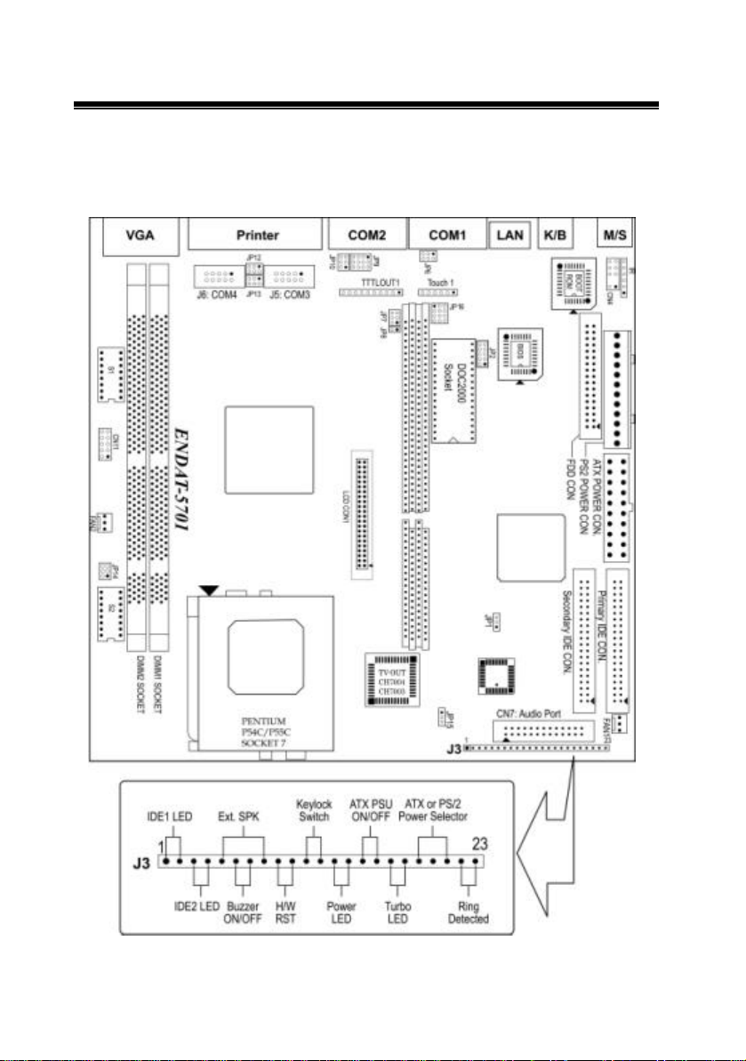
The ENDAT-5701/5901 All-In-One motherboard
Copyright Notice
The content of this manual has been checked for accuracy. The manufacturer
assumes no responsibility for any inaccuracies that may be contained in this
manual. The manufacturer reserves the right to make improvements or
modification to the this document and/or the product at any time without prior
notice. No part of this document may be reproduced, transmitted, photocopied or
translated into any language, in any form or by any means, electronic, mechanical,
magnetic, optical or chemical, without the prior written permission of the
manufacturer.
VIA is registered trademark of VIA Technology Incorporation
VIA Apollo MVP4 may only be used to identify products of VIA Technology
VT82C868A may only be used to identify products of VIA Technology
Realtek is registered trademark of Realtek Technologies Inc.
Multiscan is a trademark of Sony Corp of America
IBM, EGA, VGA, PC/XT, PC/AT, OS/2 and PS/2 are registered trademarks of
International Business Machines Corporation
Intel is a registered trademark of Intel Corporation
Plug and Play is registered trademarks of Intel Corporation
Microsoft, Windows and MS-DOS are trademarks of Microsoft Corporation
Award is a trademark of Award Software Inc.
PCI is a registered trademark of PCI Special Interest Group
Other product names mentioned herein are used for identification purpose only
and may be trademarks and/or registered trademarks of their respective
companies.
Installation Notice
The manufacturer recommends using a grounded plug to ensure proper
motherboard operation. Care should be used in proper conjunction with a
grounded power receptacle to avoid possible electrical shock. All integrated
circuits on this motherboard are sensitive to static electricity. To avoid damaging
componentsfromelectrostaticdischarge,pleasedonotremovetheboardfromthe
anti-static packing before discharging any static electricity to your body, by
wearing a wrist-grounding strap. The manufacturer is not responsible for any
damage to the motherboard due to improper operation.