Union Semiconductor UM3501EVB User manual

UM3501 EV Board User’s Guide
http://www.union-ic.com 1/10
UM3501
EV Board (Evaluation Kit)
User’s Guide
V1.0
Version Date Prvoider Approve Note
1.0 2012-05-11 Initial version.

UM3501 EV Board User’s Guide
http://www.union-ic.com 2/10
Table of Contents
1. Board Information
1.1 Schematic
1.2 PCB Layout
1.3 InterfaceDefine
2. Board Operation
2.1 Power Supply
2.2 Enable
2.3 Output Setting
3. Board Component
3.1 Input Capacitor
3.2 Output Capacitor
3.3 Inductor
3.4 Sampling Resistor
4. PCB Layout Considerations

UM3501 EV Board User’s Guide
http://www.union-ic.com 3/10
1 . Board Information
This UM3501EVB uses a UM3501 adjustable output buck converter to step down
2.5-V or higher input voltages. The EVB operates over an input voltage range of
2.5V to 5.5V. The goal of the EVB is to demonstrate the small size of the UM3501
power supply solution and provide flexibility in interchanging the supporting passive
components. This EVB include an enable jumper that allows the user to disable the
device.
1.1 Schematic
Fig 1.1 is UM3501 EVB design schematic.
SW 5
FB 4
EN
3
GND
2
VIN
1
U1
UM3501
4.7uF
C1
GND
GND
10uF
C3
2.2uH
L1
R1
R2
GND
option
C2
GND
1
2
3
EN
EN
VIN
GND
VIN VOUT
GND
GND
EN
VIN
634k
316k
Fig 1.1 UM3501 EVB schematic
(Recommended Value of R1 and R2 for 1.8V output)
1.2 PCB Layout

UM3501 EV Board User’s Guide
http://www.union-ic.com 4/10
Fig 1.2, Fig 1.3 is PCB layout and components location diagram of UM3501 EVB.
Fig 1.2 UM3501 EV board PCB top layer
Fig 1.3 UM3501 EV board PCB bottom layer

UM3501 EV Board User’s Guide
http://www.union-ic.com 5/10
1.3 Interface Define
Tab 1.1 is the directions of UM3501 EV board interface signals
Tab 1.1 UM1661 EVB board interface
Interface Function Note
VIN Power supply input.
GND Ground.
2.5V – 5.5V power supply.
EN Chip enable/disable option. EN=ON (1): enable.
EN=OFF (0): disable.
VOUT The board output. UM3501 output.
2 . Board Operation
An input power supply and a load must be connected to the appropriate EVB
connectors in order for the EVB to operate. The absolute maximum input voltage is
6V. The UM3501 is designed to operate with a maximum input voltage of 5.5 V.
Short pins 2−3 on jumper EN (labeled ON) to enable the device. Connect a load not
to exceed 600 mA to the output of the EVB. Fig 2.1 shows the output ripple and
switching waveform for UM3501’s operation. (VIN=3.6V, VOUT=1.8V, 300mA load
current).

UM3501 EV Board User’s Guide
http://www.union-ic.com 6/10
Fig 2.1 UM3501 waveform diagram (VIN=3.6V, VOUT=1.8V, ILOAD=300mA)
2.1 Power Supply
UM3501's input supply voltage range from 2.5V – 5.5V, you need to confirm there is
sufficient margin with the current limit when use a DC source to supply the device.
Input power cable should be thicker to reduce the loss of input voltage when the load
current is large.
2.2 Enable
EN jumper should be set to ON to enable the UM3501.EN jumper set to OFF to shut
down the device.
2.3 Output Setting
VOUT
SW

UM3501 EV Board User’s Guide
http://www.union-ic.com 7/10
The output voltage of UM3501 is set by the external resistor divider. See Figure
1.1.The output voltage is calculated as VOUT=0.6V×(1+R2/R1) with R1+R2≤1MΩ.
For stability, R1+R2 should not be greater than 1 MΩ. To keep the operating
quiescent current to a minimum, the feedback resistor divider should have high
impedance.
For example: Use 634 k ohms R1 and 316 k ohms R2 to get a 1.8V output.
VOUT=0.6V×(1+R2/R1)=0.6V×(1+634 /316)=1.80V
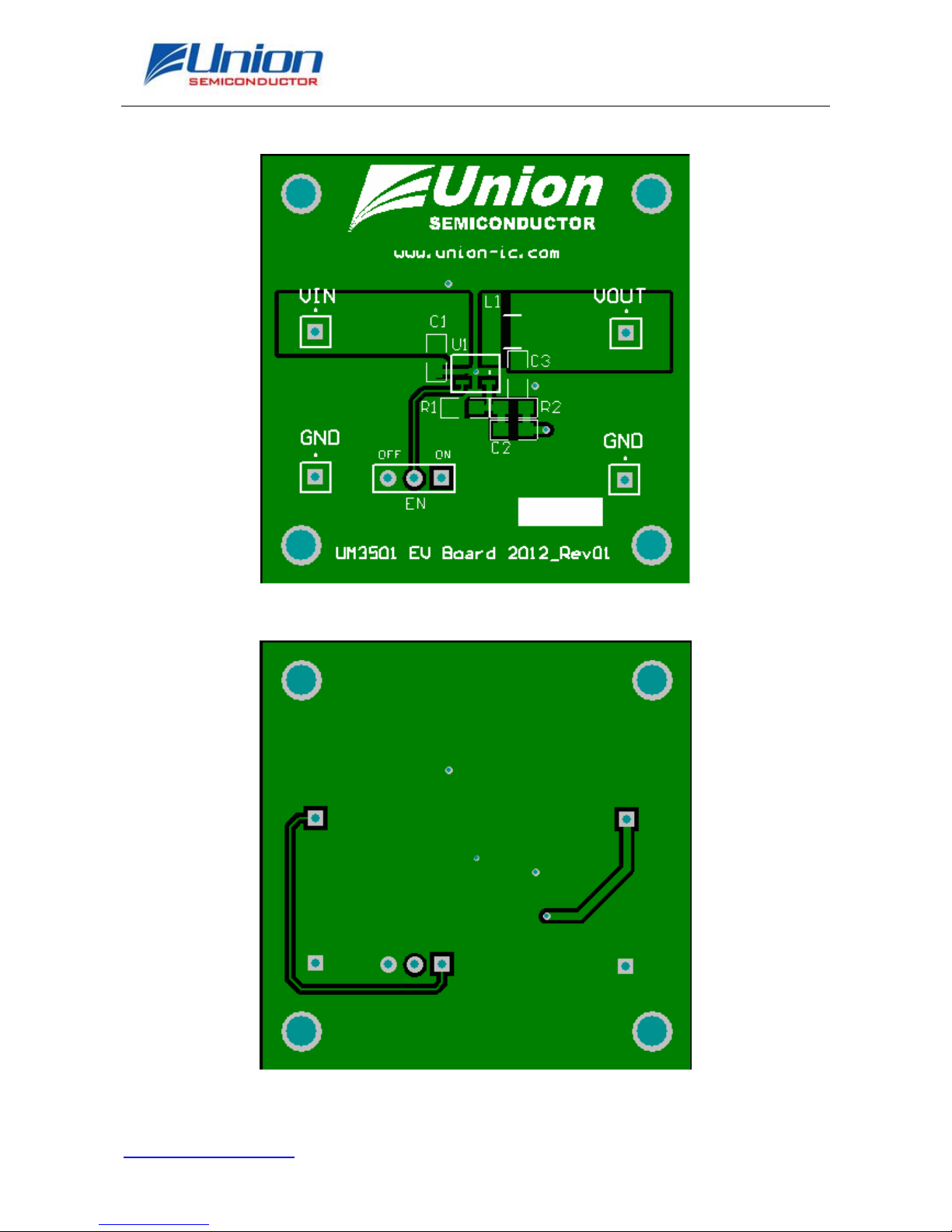
3. Board Component
Tab 3.1 is the recommended BOM list of UM3501 EV board.
Tab 3.1 UM3501 EV board recommended BOM list
Reference Description Part No. Manufacturer.
U1 Union Buck Converter. UM3501 Union
C1 Capacitor,4.7uF,6.3V,Ceramic,X5R,0805. JMK212BJ475MG Taiyo
C2 Default for UM3501 Evaluation - -
C3 Capacitor,10uF,6.3V,Ceramic,X5R,0805. C2012X5R0J106M TDK
L1 Inductor,2.2uH,850mA,33mΩ,SMT. CDRH2D18/LD-2R2 Sumida
R1,R2 Resistor, 1%,0603 or 0805 Std Std
3.1 Input Capacitor
The input capacitors reduce the current peaks drawn from the battery or input power
source and reduce switching noise in the IC. Ceramic capacitors with X5R or X7R
temperature characteristics are highly recommended due to their small size, low ESR,
and small temperature coefficients. A 4.7µF X5R or X7R capacitor (C1) from VIN to

UM3501 EV Board User’s Guide
http://www.union-ic.com 8/10
GND is recommended for most application. For optimum noise immunity and low
input ripple, the input capacitor value can be increased. Note that some ceramic
dielectrics exhibit large capacitance and ESR variation with temperature and DC bias.
Ceramic capacitors with Z5U or Y5V temperature characteristics should be avoided.
See Table 3.1 for suggested capacitors and manufacturers.
3.2 Output Capacitor
The output capacitor limits the output ripple and maintains the output voltage during
large load transitions. A 10μF X5R or X7R ceramic capacitor (C3) typically provides
sufficient bulk capacitance to stabilize the output during large load transitions and has
the ESR and ESL characteristics necessary for low output ripple. For optimum
load-transient performance and very low output ripple, the output capacitor value can
be increased; however, care should be taken with regards to output voltage slew rate
requirements. Note that some ceramic dielectrics exhibit large capacitance and ESR
variation with temperature and DC bias. Ceramic capacitors with Z5U or Y5V
temperature characteristics should be avoided. Tantalum capacitors are not
recommended. See Table 3.1 for suggested capacitors and manufacturers.
3.3 Inductor
The step-down converter operates with a typical switching frequency of 1MHz. This
operating frequency allows the use of physically small inductors while maintaining
high efficiency. A 2.2µH to 4.7µH inductor is recommended for most applications.
Inductor saturation current is another important parameter during inductor selection.

UM3501 EV Board User’s Guide
http://www.union-ic.com 9/10
Below formula shows how to calculate the actual peak inductor current under certain
application. The saturation inductor current should be higher than the calculated
value under the worse case.
ΔIL=VOUT*(VIN-VOUT)/(VIN* L *fosc)
IPEAK = ILOAD +ΔIL/2
Where ΔILis Peak-Peak inductor ripple current,
IPEAK is peak inductor current,
ILOAD is maximum load current in the application.
For example: 1.8V output at 3.6V input voltage, when choose a 2.2uH inductor, the
value of the inductor Peak current at 600mA load current can be calculated as blow:
ΔIL=VOUT*(VIN-VOUT)/(VIN* L *fosc)=1.8*(3.6-1.8)/(3.6*2.2*1)=0.409(A)
I
PEAK = IDC +ΔIL/2=0.6+0.409/2=0.805 (A)
For optimum load transient and efficiency, low DCR inductors should be selected.
See Table 3.1 for suggested inductors and manufacturers.
4. Layout Considerations
For all switching power supplies, the layout is an important step in the design,
especially at high-peak currents and switching frequencies. If the layout is not
carefully done, the regulator shows stability problems as well as EMI problems.
Good layout for the UM3501 can be implemented by following a few simple design
rules.
1) Use wide and short traces for the high current paths.

UM3501 EV Board User’s Guide
http://www.union-ic.com 10/10
2) The input capacitor, as well as the inductor and output capacitor, should be placed
as close as possible to the IC pins. In particular, the input capacitor needs to be placed
as close as possible to the IC pins, directly across the Vin and GND pin.
3) The feedback resistor network must be routed away from the inductor and switch
node to minimize noise and magnetic interference. To further minimize noise from
coupling into the feedback network and feedback pin, the ground plane or ground
traces must be used for shielding.
Table of contents
Popular Motherboard manuals by other brands

Xilinx
Xilinx Virtex-7 FPGA VC7222 IBERT Getting started guide

Analog Devices
Analog Devices EVAL-AD7605-4SDZ user guide

Texas Instruments
Texas Instruments TI CC3000 user guide

ON Semiconductor
ON Semiconductor NB3H63143G manual

Texas Instruments
Texas Instruments TMDS1204EVM user guide

ASROCK
ASROCK M3N78D installation guide