Vantron VT-SBCQ7-MX6Q User manual

VT-SBCQ7-MX6Q Boards User’s Manual
VT-SBCQ7-MX6Q
User’s Manual
(Hardware)
Chengdu Vantron Technology Ltd. Co.

VT-SBCQ7-MX6Q Boards User’s Manual
All rights reserved Page 2, Total 30
Revision record
Date
Version
Change Description
2018-06-14 1.0 Initial Version
2018-07-30 2.0 Modified Display description

VT-SBCQ7-MX6Q Boards User’s Manual
All rights reserved Page 3, Total 30
Table of Contents
1.1 COPYRIGHT NOTICE ......................................................................................................................................................4
1.2 NOTES ..........................................................................................................................................................................4
1.3 STATEMENT ..................................................................................................................................................................4
1.4 DISCLAIMER..................................................................................................................................................................4
1.5 LIMITATION OF LIABILITY/NON-WARRANTY....................................................................................................................4
1.6 SAFETY INSTRUCTIONS ..................................................................................................................................................5
1.7 PRECAUTIONS...............................................................................................................................................................5
1.8 SAFETY INSTRUCTIONS FOR POWER CABLES AND ACCESSORIES .......................................................................................5
2OVER VIEW .......................................................................................................................................................................7
2.1 INTRODUCTION.............................................................................................................................................................7
3SBCQ7-MX6Q HA RDWA RE INS TRUC TIONS ................................................................................................................8
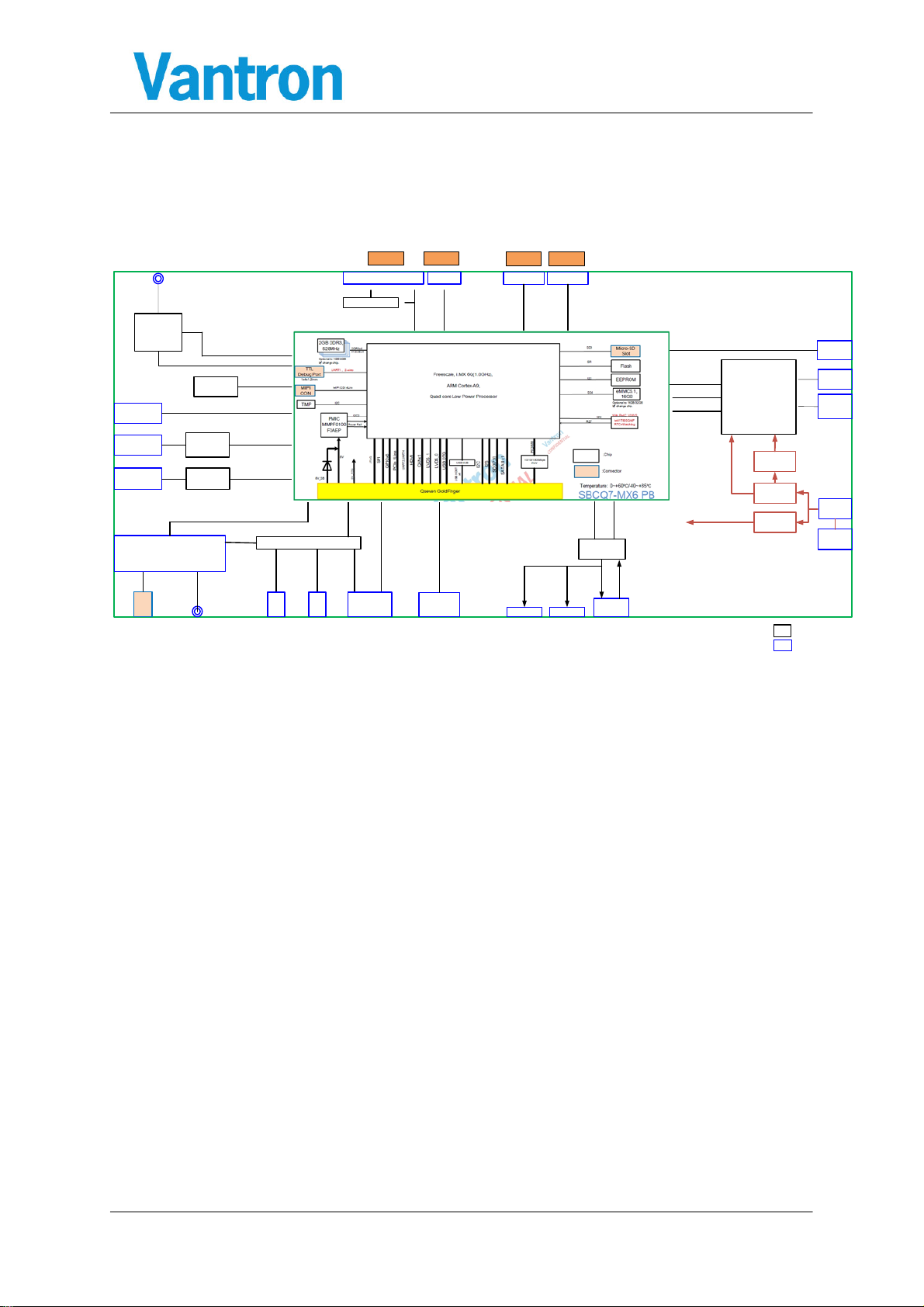
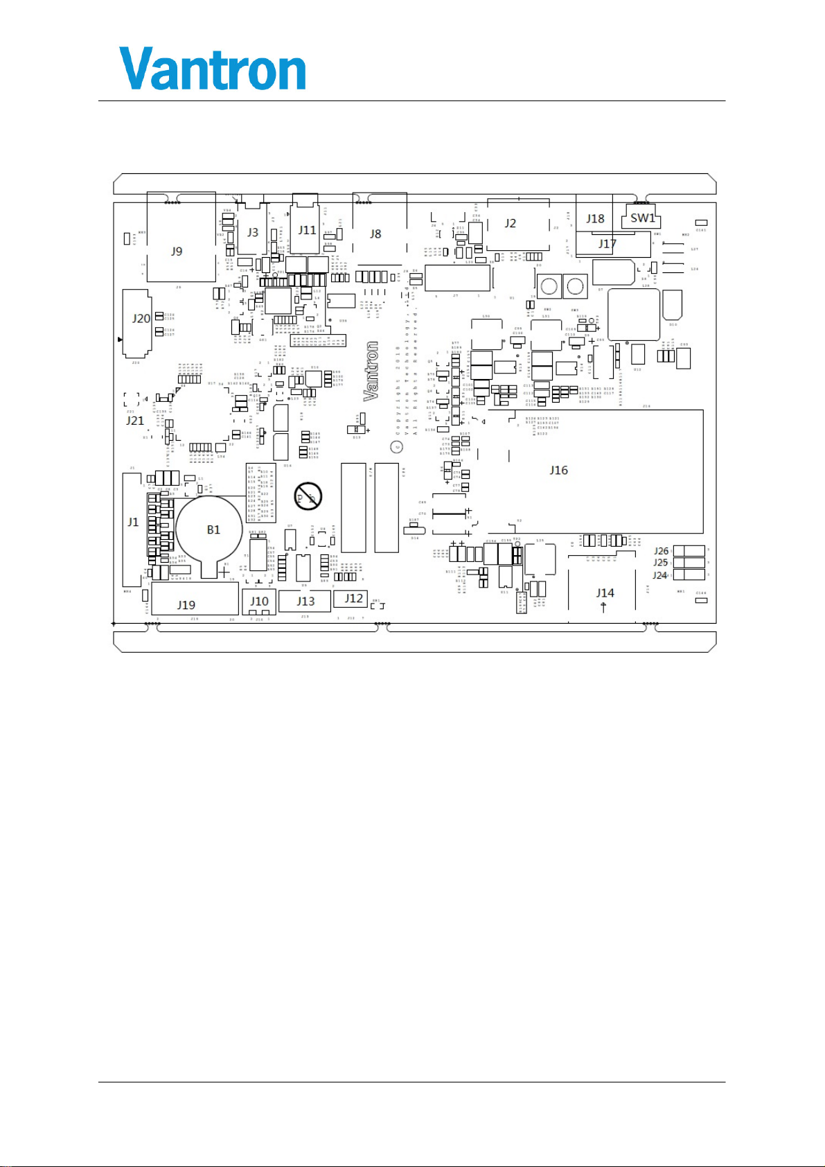
3.1 BOARD DIAGRAM .........................................................................................................................................................8
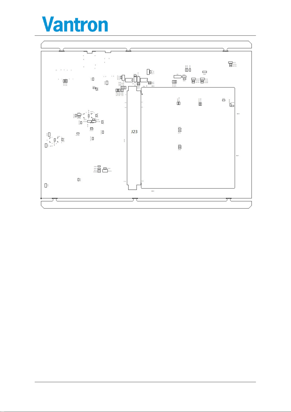
3.2 BOARD ASSEMBLY DRAWING ........................................................................................................................................9
3.3 BOARD STRUCTURE.................................................................................................................................................... 11
4HARDWARE DESCRIP TION .......................................................................................................................................... 13
4.1 IDENTIFY CONNECTOR ................................................................................................................................................ 13
4.1.1 Position of connector.................................................................................................................................. 13
4.1.2Confirm the pin direction ........................................................................................................................... 13
4.2 SWITCH,BUTTONS,JUMPERS,LEDS........................................................................................................................... 13
4.2.1 S1 Boot Settings ........................................................................................................................................... 13
4.2.2 B1, RTC Ba ttery ............................................................................................................................................ 13
4.3 LCD,DISPLAY............................................................................................................................................................. 14
4.4 TP,TOUCH PANEL....................................................................................................................................................... 14
4.5 CONNECTORS DESCRIPTION........................................................................................................................................ 14
4.5.1 J1, LCD display port ..................................................................................................................................... 15
4.5.2 J2, HDMI port ............................................................................................................................................... 16
4.5.3 J3,Audio port ................................................................................................................................................ 17
4.5.4 J4&J5, Speaker port..................................................................................................................................... 17
4.5.5 J6, Micro US B Port ....................................................................................................................................... 17
4.5.6 J7, Internal USB port ................................................................................................................................... 17
4.5.7J8,Internal USB port .................................................................................................................................... 18
4.5.8 J9, 10/100/1000M Ethernet port.............................................................................................................. 18
4.5.9 J10,CAN port................................................................................................................................................. 18
4.5.10 J11,Debug UART Connect port .................................................................................................................. 18
4.5.11 J12,JTAG port ............................................................................................................................................... 18
4.5.12 J13,RS232 port............................................................................................................................................. 19
4.5.13 J14, SIM card slot......................................................................................................................................... 19
4.5.14 J15,SATA Power connector ........................................................................................................................ 19
4.5.15 J16,MINI-PCIE conne cto r............................................................................................................................ 19
4.5.16 J17,power supply port ................................................................................................................................ 20
4.5.17 J19,Reserve port .......................................................................................................................................... 20
4.5.18 J20 ,SATA....................................................................................................................................................... 21
4.5.19 J21, RF antenna for WiFi&BT..................................................................................................................... 21
4.5.20 J64, Backlight ............................................................................................................................................... 21
4.5.21 J23, 230 pin Gold-Finger............................................................................................................................. 21
4.6 HARDWARE OPERATION NOTES ................................................................................................................................. 28
5TIP S .................................................................................................................................................................................. 29

VT-SBCQ7-MX6Q Boards User’s Manual
All rights reserved Page 4, Total 30
1.1 Copyright Notice
While all information contained herein have been carefully checked to assure its accuracy in
technical details and printing, Vantron assumes no responsibility resulting from any error or features
of this manual, or from improper uses of this manual or t he software. Please cont act our tec hnical
department for relevant operation solutions if there is any problem that cannot be solved according to
this manual.
Vantron reserves all rights of this manual, including the right to change the content, form, product
features, and specifications contained herein at any time without prior notice. The latest version of
this manual is at www.vantrontech.com.cn. Please contact Vantron for further information:
Vantron Technology(Vantron)
E-mail: sales@vant ront ech.com
The tradem arks and registered trademarks in this manual are properties of their respective owners.
No part of this manual m ay be copied, reproduced, translated or sold. No changes or other purposes
are permitted without the prior written cons ent of Vantron.
Vantron reserves the right of all publicly-released copies of this manual.
1.2 Notes
Applicable notes are listed in the following table:
Sign Notice
Type Description
Notice Important information and regulations
Caution Cauti on for latent damage t o
system or
harm to personnel
1.3 Statement
It is recommended to read and comply with this manual before operating board, which provides
important guidance and helps decreasing the danger of injury, electric shock, fire, or any damage to
the device.
1.4 Disclaimer
Vantron assumes no legal liability of accidents resulting from failure of conforming to the safety
instructions.
1.5 Limitation of Liability/Non-warranty

VT-SBCQ7-MX6Q Boards User’s Manual
All rights reserved Page 5, Total 30
For di rect or indirect damage to this device or other devices of Vantron caused by failure of
conforming to this manual or the safety instructions on device label, Vantron assumes neither
warranty nor legal liability even if the device is still under warranty.
1.6 Safety Instructions
Keep and comply wit h all operation instructions, warnings, and inform ation.
Pay attention to warnings on this device.
Read the following precautions so as to decrease the danger of injury, electric shock, fire, or any
damage to the device.
1.7 Precautions
Pay attention to the product labels/safety instructions printed on silk screens.
Do not try repairing this product unless declared in this manual.
Keep away from heat source, such as heater, heat dissipater, or engine casing.
Do not insert other items into the slot (if any) of this device.
• Keep the ventilation slot ventilated for cooli ng.
•System fault may arise if other items are inserted into this device.
Installation: ensure correct installation according to instructions from the manufacturer with
recommended installation tools.
Ensure ventil ation and smoothness according to relevant ventilation standard.
1.8 Safety Instructions for Power Cables and Accessories
Proper power source only
Start only with power sourc e that satisfies voltage label and the voltage nec essary according to this
manual. Please contact technical support personnel of Vantron for any uncertainty about the
requirements of necessary power source.
Use tested power sourc e
This product still contains a button lithium battery as a real-time clock after its external power source
is removed and therefore should not be short-circuited during transportation or placed under high
temperature.
Place cables properly:
Do not place cables at any place with extrusion danger.

VT-SBCQ7-MX6Q Boards User’s Manual
All rights reserved Page 6, Total 30
Cleaning Instructions
Please power off before cleaning the device.
Do not use spray det ergent.
Clean with a damp cloth.
Do not try cleaning exposed el ectronic components unless with a dust collector.
Support for special fault: Power off and contact technical support personnel of Vantron in cas e of
the following faults:
The device is damaged.
The temperature is excessively high.
Fault is still not solved after the operation according to the manual.

VT-SBCQ7-MX6Q Boards User’s Manual
All rights reserved Page 7, Total 30
2Over View
2.1 Introduction
Vantron offers both ARM and ATOM based Single Boards Computer (SBC) platforms
including Cirrus Logic EP9315, Marvell PXA255, PXA270, and PXA320, Intel IXP465, FreeScale
iMX31, Imx53,iMX6, Samsung S3C6410, TI OMAP35xx CortexA8 series, and Intel ATOM Z510
and Z530 processor boards. In additional to offering the standard SBCs, we also provide
professional customization board design services. Our seamless project management, efficient
error-free development process, strong fundamentals in technology, sufficient in human
resources, and on-time delivery will guarantee the success in your project development.
Based on idea of “Application Ready” products and services, our embedded computers have
embedded basic operation system which includes the drivers of its interfaces. So it is easy to be
used by adding your application software only. It can speed Time to Market of your products, and
saving more cost.
SBCQ7-MX6Q is an A9 processor based board with 9” LCD display.
And the function such as:
Freescale IMX6Q,1GHz,Low Power Processor.
With a 1280x240 TFT-LED
With a touch panle
Supports 802.11b,g,n WiFi 2.4GHz and Bluetooth 4.1
Embedded Linux, Android ,WinCE, Supported

VT-SBCQ7-MX6Q Boards User’s Manual
All rights reserved Page 8, Total 30
3SBCQ7-MX6Q Hardware Instructions
3.1 Board Diagram
USB OTG
TYPE-C
USB TYPEC OTG
Power Rail
I2C2
U.FL connector for
external antenna
Accel
(3-axis)
Debug Port
Jack
UART1,2-wires
PMIC
TPS659114
+System power PWRKEY
Reset
SIM
Slot
#1
SDIO WiFi &
Bluetooth
Module
AP6255
Headphone
Audio Codec
WM8960
I2C1
I2S
MIC
Power Rail
USB 3.0
RGMII
RJ45
USB3
USB4
UART2,2-wires
Type-A
I2C2
SDIO0
UART5
BT4.1
802.11a/b/g/n/ac
CON
eDP-2xLVDS
1x6x2.54
eDP
HDMI OUT
TP,I2C4
MINI-PCIE
PCIE
HUB
USB2.0 HOST1
USB2
USB1
1x2x2.54
1x2x2.54
SPK-L
SPK-R
Audio
JACK
Power
Jack
DC-DC
TPS5450
12V input
(8-17V Range)
DC-DC
RT8299
3.3V
1x6x2.54
DC-DC
TPS62136
3.3V
5V
For 3/4G and PCIE device
: IC Chip
: Connector
Type-A,RA
Dual USB
1x4x
1.25
1x4x
1.25
1x30x0.5
MIPI
Camera
Touch
Display
Display
RS232
TJA1040CAN
CAN
RS232

VT-SBCQ7-MX6Q Boards User’s Manual
All rights reserved Page 9, Total 30
3.2 Board Assembly Drawing
Top view

VT-SBCQ7-MX6Q Boards User’s Manual
All rights reserved Page 10, Total 30
Bottom view

VT-SBCQ7-MX6Q Boards User’s Manual
All rights reserved Page 11, Total 30
3.3 Board Structure

VT-SBCQ7-MX6Q Boards User’s Manual
All rights reserved Page 12, Total 30

VT-SBCQ7-MX6Q Boards User’s Manual
All rights reserved Page 13, Total 30
4Hardware Description
This chapter describes the hardware Features, include switch, jumper, connector and PIN
function
The interface description ought to consult the connector sketch map. And attach
necessary message such as picture. Indicate the figure, PIN1 and match jack
4.1 Identify connector
This section describes how to find the position of connector and PIN1 on
SBCQ7-MX6Q-COMBI single computer board.
4.1.1 Position of connector
As Figure 3.2 show the main part and connector position of SBCQ7-MX6Q-COMBI.
4.1.2 Confirm the pin direction
There is the pin number order in all Vantron’s
product, this picture at right indicate each pin’s
number, that message as show on the top
side(component side) of main board. on double row
connector, one side is naming odd number and another
side is naming even number. Please according to below method to confirm the Pin1 of
connector and jumper:
1. Usually, there is any number and mark at side ofconnector in main board, such as
trigonal mark, dot and number “1” all indicate the pin1 of connector
2. About the hole connector, you can see pin number on the reversed side
3. Download the SBCQ7-MX6Q mechanism from Vantron technology sustain or Vantron
net site: www.vantrontech.com
4.2 Switch, Buttons, Jumpers, LEDs
This section describes the setting of switch, controller, LED on SBCQ7-MX6Q board.
4.2.1 S1 Boot Settings
SBCQ7-MX6Q support three kinds of boot up method, by 2 bit DIP Switch(S1). It can be
boot up form USB OTG,SD Card, eMMC.
Start up method
SYS_BOOT[1:0]
SD Card 1 0
eMMC 0 1
USB OTG 0 0
4.2.2 B1, RTC Battery
B1 is for RTC Battery. The suggest part is BR1225A from PANASONIC.

VT-SBCQ7-MX6Q Boards User’s Manual
All rights reserved Page 14, Total 30
4.3 LCD,display
General specification of the 7” LCD.
Item Feature Spec
Characteristics
Resol ution 1280(RGB)x 240
Pixel Pitch 0.17475x0.17475
Pixel Configuration R.G.B Vertical Stripe
LED Numbers 40 LEDs
Interface LVDS
Color Depth 16.7M
4.4 TP,touch panel
7" TP/5071-TM-FP GEN2,I2C,3.3V,1.77mm,6H,-20~60℃
Pin Nam e Description
1 VCC 5V
2 D- USB DATA-
3 D+ USB DATA+
4 GND Ground
5 GND Ground
4.5 Connectors Description
This table is the respective describe valid signal of connector on SBC-Q7-MX6Q
board.
Figure type:
N/C Not connect
GND Ground
/ active low signal
+ Positive of difference signal
- negative of differenc e signal
Signal type:
I Input
O Output
IO input/out put
P Power or ground
A Analog
OD Open drain

VT-SBCQ7-MX6Q Boards User’s Manual
All rights reserved Page 15, Total 30
4.5.1 J1, LCD display port
1x40,0.5mm,0.5A,1.05mm,M,RA,WDT,SMT,RoHS (JAE: HD1S040HA1)
Pin
Name
Type
Description
1LCD_VDD P LCD digital power supply +3.3V
2
LCD_VDD P LCD digital power supply +3.3V
3LCD_VDD P LCD digital power supply +3.3V
4RST O TP Reset
5LVDSA_DATA#0_R O EDP/LVDSA data
6LVDSA_DATA0_R O EDP/LVDSA data
7GND P Ground
8LVDSA_DATA#1_R O EDP/LVDSA data
9LVDSA_DATA1_R O EDP/LVDSA data
10 GND P Ground
11
LVDSA_DATA#2_R O EDP/LVDSA data
12 LVDSA_DATA2_R O EDP/LVDSA data
13 GND P Ground
14 LVDSA_CLK #_R O EDP data/LV DSA clock
15 LVDSA_CLK_ R O EDP data/LV DSA clock
16 GND P Ground
17 LVDSA_DATA#3_R O EDP/LVDSA data
18
LVDSA_DATA3_R O EDP/LVDSA data
19 INT I TP Interrupt
20 LVDSB_DATA#0_R O LVDSB data
21 LVDSB_DATA0_R O LVDSB data
22 GND P Ground
23 LVDSB_DATA#1_R O LVDSB data
24 LVDSB_DATA1_R O LVDSB data
25 GND P Ground
26 LVDSB_DATA#2_R O LVDSB data
27
LVDSB_DATA2_R O LVDSB data
28 GND P Ground
29
LVDSB_CLK #_R O LVDSB clock
30 LVDSB_CLK_ R O LVDSB clock
31 GND P Ground
32 LVDSB_DATA#3_R O LVDSB data

VT-SBCQ7-MX6Q Boards User’s Manual
All rights reserved Page 16, Total 30
33 LVDSB_DATA3_R O LVDSB data
34 LVDS_BKLTEN O LCD backlight enabl e signal
35 LVDS_BKLTCTL O LCD backlight PWM signal
36
LVDS_DDC_ CLK_R O I2C clock
37 LVDS_DDC_ DATA_R IO I2C data
38 LCD_BLK P LCD backlight power supply +5V
39 LCD_BLK P LCD backlight power supply +5V
40 LCD_BLK P LCD backlight power supply +5V
4.5.2 J2, HDMI port
Type A,NoFLN,F,RA,-20~85℃,SMT,RoHS (MOLEX: 47151-1001)
Pin
Name
Type
Description
1HDM I_D 2P O HDMI Data2+
2GND P Ground
3HDM I_D 2N O HDM I Data2-
4HDM I_D 1P O HDMI Data1+
5GND P Ground
6
HDM I_D 1N O HDM I Data1 -
7HDM I_D 0P O HDMI Data0+
8
GND P Ground
9HDM I_D 0N O HDM I Data0 -
10 HDM I_C LKP O HDM I CLK+
11 GND O Ground
12 HDM I_C LKN O HDM I CLK-
13 HDM I_CE C_O UT I
14 NC O NC
15 H_CLK_OUT O HDM I C LK OUT
16 H_DAT_OUT O HDM I DATA O UT
17 GND P Ground
18 HDM I+5V P Power Supply
19 HP_DET_OUT I HP detect
20 GND P Ground
21 GND P Ground
22 GND P Ground
23 GND P Ground

VT-SBCQ7-MX6Q Boards User’s Manual
All rights reserved Page 17, Total 30
4.5.3 J3,Audio port
3.6mm,4Pole+1Switch,1Port,F,RA,CMT,THR,RoHS (HITCONN: PJ-3106H-1)
Standard audio jack with Headphone and M IC
Pin
Name
Type
Description
2MIC_ RAW O MIC
4HP_L O Headphone left channel
6
HP_R O Headphone right channel
7HEADP HO NE_DET I Headphone detect
3 GND P Ground
4.5.4 J4&J5, Speaker port
Support 2.5W/4Ωspeaker
1x2,2.5mm,3A,7mmH,M,Vert,-25~85℃,THR,RoHS (NSXD: S2501WV-2P)
Pin
Name
Type
Description
J4-1 SPKPL O
Speaker left channel
J4-2 SPKNL O
J5-1 SPKNR O
Speaker right channel
J5-2 SPKPR O
4.5.5 J6, Micro USB Port
2.0,Micro AB,1Port,F,RA,-30~85℃,SMT,RoHS
Pin
Name
Type
Description
1 USB_OTG_CON_VBUS P USB_OTG Power detect
2 USB_OTG_CON_ DN O USB_OTG Data-
3 USB_OTG_CON_ DP O USB_OTG Data+
4 USB_OTG_ID I USB_OTG ID
5 USB_OTG_CON_GND P Ground
4.5.6 J7, Internal USB port
1x4,2.5mm,3A,7.0mmH,M,Vert,IND,THR,RoHS (ATOM: AWF-2540104-D08)
Pin
Name
Type
Description
1、2 USBH0_ GND P Ground
3 USBH0+ IO USB Data0+
4 USBH0- IO USB Data0-
4 USBH0_V CC P USB power

VT-SBCQ7-MX6Q Boards User’s Manual
All rights reserved Page 18, Total 30
4.5.7 J8,Internal USB port
2.0,TYPE A,1Port,F,RA,CMT,THR,RoHS
Pin
Name
Type
Description
A1 USBH3_V CC P USB power
A2 USBH3- IO USB Data3-
A3 USBH3+ IO USB Data3+
A4 USBH3_ GND P Ground
B1 USBH2V CC P USB power
B2 USBH2- IO USB Data2-
B3 USBH2 IO USB Data2+
B4 USBH2_ GND P Ground
4.5.8 J9, 10/100/1000M Ethernet port
10/100/1000,MAG,2LED,1Port,SHLD,F,RA,-40~85℃,THR,RoHS
(UNE: U50(02-02)G8-09-A122-B12)
4.5.9 J10,CAN port
1x2,2.5mm,3A,7mmH,M,Vert,-25~85℃,THR,RoHS
Pin
Name
Type
Description
1 CAN0_HIGH IO CAN Data
2 CAN0_LOW IO CAN Data
4.5.10 J11,Debug UART Connect port
3.6mm,3Pole,1Port,F,RA,CMT,THR,RoHS (KBIT: PJ-320F)
Matched debug cable PN: YC1083R035
Pin
Name
Type
Description
1 GND P Ground
2 TXD O Data Transmit
3 RXD I Data Receive
4.5.11 J12,JTAG port
2x4,2x2mm,2A,4.7mmH,M,Vert,WDT,SMT,RoHS
Pin
Name
Type
Description
1 JTAG_TCK I Clock Input
2 JTAG_TDI I Data Input

VT-SBCQ7-MX6Q Boards User’s Manual
All rights reserved Page 19, Total 30
3 JTAG_TDO O Data Output
4 JTAG_TMS I Mode Select
5 JTAG_TRST# I Reset
6 JTAG_TRST# I Reset
7 GND_3V3 P Power Supply
8 GND P Ground
4.5.12 J13,RS232 port
1x5,2.0mm,2A,6mmH,M,Vert,WDT,THR,RoHS
Pin
Name
Type
Description
1 GND P Ground
2 RXD2/RS485_2_A I RS232 Data Rec eive/RS485_A
3 TXD2/RS 485_2_B O RS232 Data Transmit/RS485_B
4 RST2 IO Request to Transfer
5 CTS2 IO Clear to Send
4.5.13 J14, SIM card slot
Micro,Push-Push,6P,WDT,SMT,RoHS (CSCONN: CSI06127135002)
Pin
Name
Type
Description
1 PCIE_UIM_PWR P Power Supply
2 PCIE_UIM_RST I SIM Res et
3 PCIE_UIM_ CLK I SIM Clock
5 GND P Ground
6 PCIE_UIM_VPP IO SIM Vpp power
7 PCIE_UIM_DATA IO SIM Dat a
4.5.14 J15,SATA Power connector
1x4,2.5mm,3A,7.0mmH,M,Vert,IND,THR,RoHS
Pin
Name
Type
Description
1 +12V P Power Supply
2 GND P Ground
3 GND P Ground
4 +5V P Power Supply
4.5.15 J16,MINI-PCIE connector
Mini,52P,0.8mm,6.8mmH,WDT,SMT,RoHS (TYCO: 2041262-1)

VT-SBCQ7-MX6Q Boards User’s Manual
All rights reserved Page 20, Total 30
Support kinds of 3G/4G module with USB interface
4.5.16 J17,power supply port
2mmd,6mmd,3A,12V,M,NoLock,RA,-25~85℃,THR,RoHS
(HITCONN: DC-044A-2.0-PU)
Pin
Name
Type
Description
1 12V-IN+ P Type 12V power input (Range:8-16V)
2 12V-IN+ P Type 12V power input (Range:8-16V)
3 12V-IN+ P Type 12V power input (Range:8-16V)
4 12V-IN- P Ground
5 12V-IN- P Ground
6 12V-IN- P Ground
4.5.17 J19,Reserve port
2x10,2x2mm,1.5A,4.6mmH,F,Vert,WDT,SMT,RoHS
Pin
Name
Type
Description
1 GEN_3V3 P Power
2 LVDS1_EDID_SDA IO LVDS1_EDID_Data
3 PWR_ON IO Power key reserved
4 LVDS1_EDID_SCL IO LVDS1_EDID_Clock
5 I2S0_RST#
I2S0_ Reset
6 GND P Ground
7 SEL68 O TP RST
8 I2C2_SCL_CON IO LVDS1_EDID_Data
9 SDIO_CD# IO SDIO_CD#
10 I2C2_SDA_CON IO LVDS1_EDID_Clock
11 SPI0_MISO IO SPI0_Master in slave out
12 SDIO_ACT# IO SDIO_ACT#
13 SPI0_MOSI IO SPI0_Master out slave in
14 SPI0_CS0#
SPI0_CS 0#
15 SPI0_SCLK IO SPI0_Clock
16 SPI0_CS1#
SPI0_CS1#
17 SPI0_SCLK IO SPI0_Clock
18 GEN_3V3 P 3.3V POWE R
19 GPIO3 IO TP INT
Table of contents
Other Vantron Motherboard manuals
Popular Motherboard manuals by other brands

Global American Inc.
Global American Inc. 3308040A user manual

Asahi KASEI
Asahi KASEI AK5704 manual

Global American Inc.
Global American Inc. 2808060 user manual

Ublox
Ublox EVK-VERA-P174 user guide

Simons Voss
Simons Voss SmartStick AX quick guide

Sys Tec Electronic
Sys Tec Electronic PLCcore-5208 user manual

Global American Inc.
Global American Inc. 2808310 user manual

First International Computer
First International Computer AN11 manual

Global American Inc.
Global American Inc. 3308180 user manual

Multitech
Multitech CommPlete RAS96 Upgrade guide

Global American Inc.
Global American Inc. 2808120 user manual

MSI
MSI MAG B660M MORTAR WIFI DDR4 user guide