www.vishay.com
2
Document Number: 65172
S09-1350-Rev. A, 20-Jul-09
Vishay Siliconix
SiC413DB
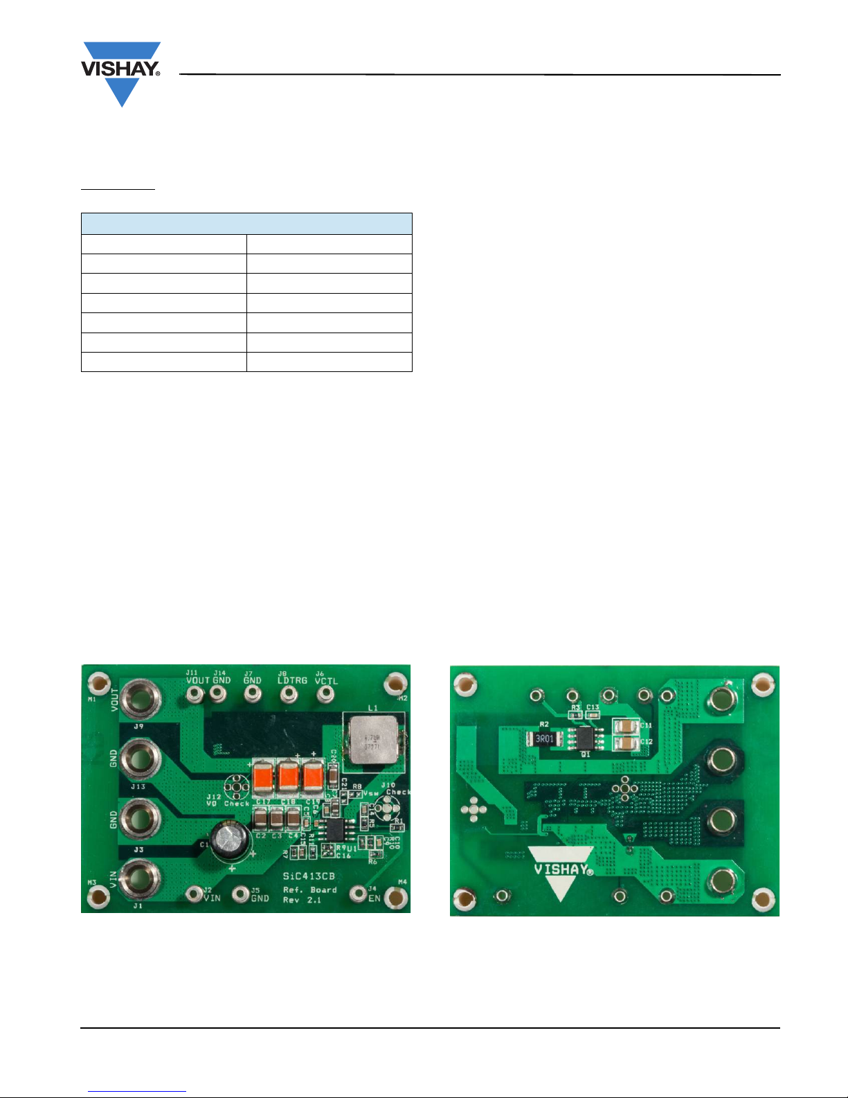
THE REFERENCE BOARD
This reference board allows the end user to evaluate the
SiC413 chip for its features and all functionalities. It can also
be a reference design for a user’s application.
SPECIFICATION
Input voltage (V): 4.75 to 24
Output voltage (V): 0.6 to 12.0
Output current (A): 0 to 4
Notes:
• This board is, by default, preset to 3.3 V output with 12 V input
• This board can be set to any output voltage between 0.6 V and
12 V, and any input voltage between 4.75 V and 24 V. For a
specific input/output voltage combination, the values of inductor
and compensation network may need to be modified and the
output capacitors may need an increase or decrease.
INPUT CAPACITORS
The input capacitors are chosen as a combination of
electrolytic and ceramics so that the capacitance, the rms
current, the ESR, the input voltage ripple and the cost can
be all fairly satisfied. For a combination of high voltage input
and low voltage output (low duty cycle), the electrolytic
capacitors (C1) may not be required.
INDUCTORS
If off-the-shelf inductors are to be used, then their DCR and
saturation current parameters are the key besides their
inductance values. The DCR causes an I2R loss, which will
decrease the system efficiency and generate heat on the
board. The saturation current has to be higher than the
maximum output current plus ripple current. In over current
condition the inductor current may be drastically high. All
these need to be put into consideration when selecting the
inductor.
On this board Vishay IHLP4040DZ series inductors are
used to meet cost requirement and get better efficiency.
OUTPUT CAPACITORS
Voltage, ESR, rms current capability and capacitance are
essential elements to consider when choosing output
capacitors. The ESR and capacitance affect the output
voltage ripple, transient response and system stability. The
rms current capability determines the capacitor power
dissipation and life time. To meet all the 4 element
requirements, combination of ceramics and tantalum can be
used.
CONNECTION AND SIGNAL/TEST POINTS
Power sockets
VIN (J1), GND (J3): Input voltage source with VIN to be
positive. Connect to a 4.75 V to 24 V source that powers
SiC413.
VOUT (J9), GND (J13): Output voltage with VOUT to be
positive. Connect to a load that draws less than 4 A current.
Signal and test leads
VIN (J2), GND (J5): Intput voltage sense pins with VIN to be
positive. Connect to a volt meter or an oscilloscope probe if
display or waveform is needed.
VOUT (J11), GND (J14): Output voltage sense pins with
VOUT to be positive. Connect to a volt meter or an
oscilloscope probe if display or waveform is needed.
VCTRL (J6), LDTRG (J8), GND (J7): Load step control signal
input. Connect VCTRL and GND to a power source, VEXT
,
which supplies enough voltage to generate the load step
needed. Connect LDTRG and GND to a pulse generater
that creates the MOSFET on/off signal for the load step.
EN: SiC413 enable signal input. To enable the system leave
this point open, otherwise connect it to any GND.
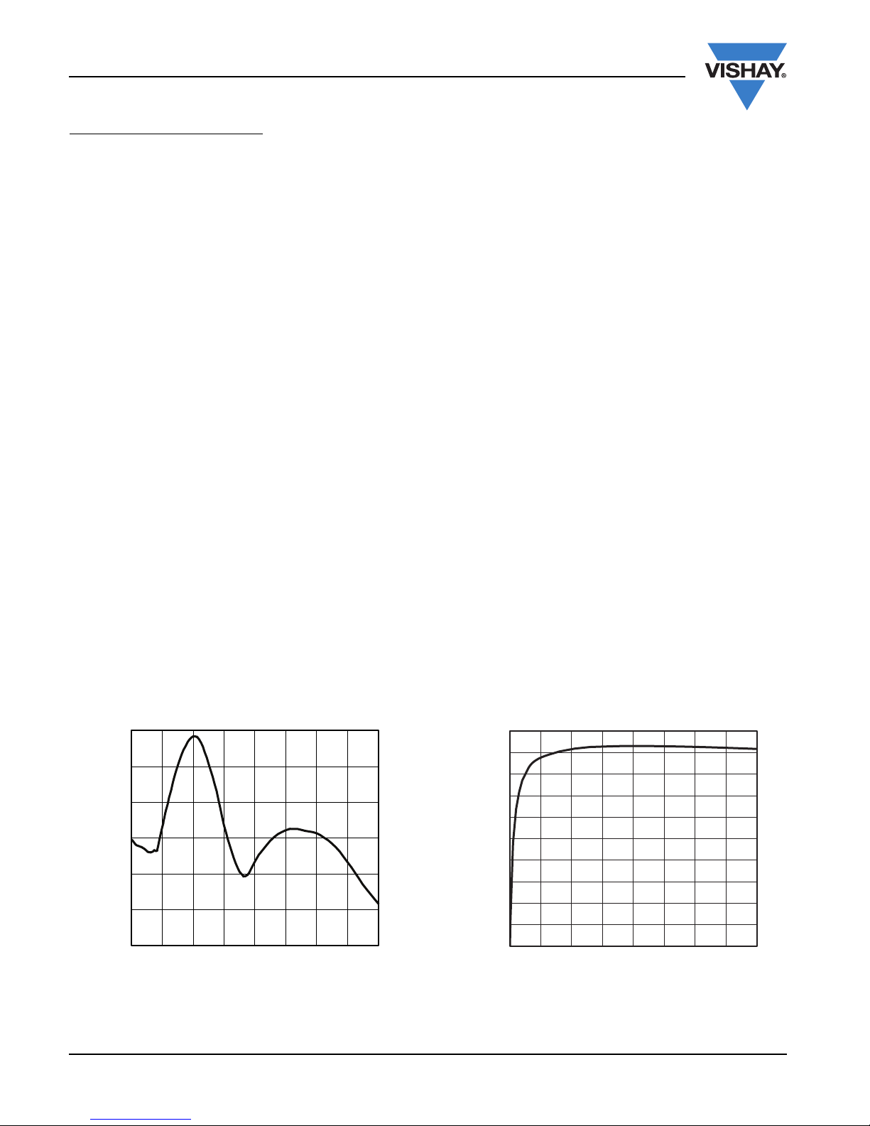
Figure 3. 12 V - 3.3 V Load Regulation
- 0.3
- 0.2
- 0.1
0
0.1
0.2
0.3
0.0 0.5 1.0 1.5 2.0 2.5 3.0 3.5 4.0
Load Current (A)
Output Voltage Variation (%)
Figure 4. 12 V - 3.3 V Efficiency
0
10
20
30
40
50
60
70
80
90
100
0.0 0.5 1.0 1.5 2.0 2.5 3.0 3.5 4.0
Load Current (A)
Efficiency (%)