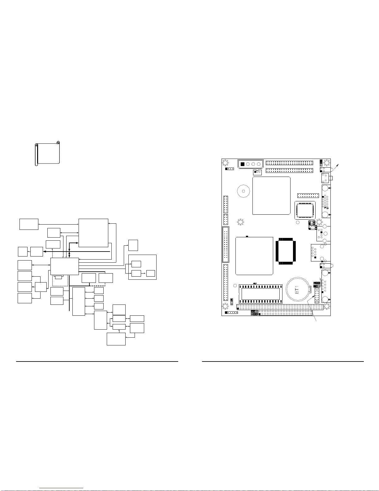
Vox WAFER-5820 User manual

WAFER-5820
Low Power GXLV-233 MMX
with SVGA/LCD,
Ethernet, & Audio SBC.
Copyright Notice
©Copyright 2000. All Rights Reserved. Manual first edition Apr..01, 2000.
The information in this document is subject to change without prior notice in order to
improve reliability, design and function and does not represent a commitment on the part
of the manufacturer.
In no event will the manufacturer be liable for direct, indirect, special, incidental, or
consequential damages arising out of the use or inability to use the product or
documentation, even if advised of the possibility of such damages.
This document contains proprietary information protected by copyright. All rights are
reserved. No part of this manual may be reproduced by any mechanical, electronic, or
other means in any form without prior written permission of the manufacturer.
Trademarks
WAFER-5820 is a registered trademark. IBM PC is a registered
trademark of International Business Machines Corporation. Intel is a registered
trademark of Intel Corporation. Other product names mentioned herein are used for
identification purposes only and may be trademarks and/or registered trademarks of their
respective companies
2
Contents
1.Introduction.........................................................................4
1.1 Specifications
1.2 What You Have
2.Installation...........................................................................7
2.1 Wafer-5820 Block Diagram & Board Layout
2.2 Unpacking Precautions
2.3 System Memory DRAM
2.4 Watch-Dog Timer Setting
2.5 Clear CMOS Setup
2.6 COM2 Setting JP12 , JP13
2.7 LCD Vcc Voltage Selector
2.8 DiskOnChip™ Flash Disk Memory Address setting
3.Connection........................................................................12
3.1 Floppy Disk Drive Connector (CN7)
3.2 PCI E-IDE Disk Drive Connector (CN2)
3.3 Parallel Port (CN1)
3.4 Series Ports (CN8, CN9)
3.5 Audio Connector
3.6 Keyboard & PS/2 Mouse Connector (CN6)
3.7 USB Port Connector CN5
3.8 IrDA Infrared Interface Port (CN11)
3.9 VGA Connector (CN4)
3.10 LCD/LVDS Interface Connector
3.11 LAN RJ45 Connector
3.12 Fan Connector (FAN1)
3.13 External Power Connector
3.14 PC/104 Connection Bus
3.15 Ethernet LED and Power/HDD LEDS

3
4.AWARD BIOS Setup ..........................................................25
4.1 Getting Start
4.2 Standard CMOS Setup
4.3 BIOS Features Setup
4.4 Chipset Features Setup
4.5 Power Management Setup
4.6 PNP / PCI CONFIGURATION
4.7 LOAD BIOS DEFAULTS
4.8 LOAD SETUP DEFAULTS
4.9 INTEGRATED PERIPHERALS
4.10 SUPERVISOR PASSWORD AND USER PASSWORD
4.11 IDE HDD AUTODETECTION
5.SVGA Setup.......................................................................37
5.1 Introduction
5.2 Further Information
6.Audio..................................................................................39
6.1 Introduction
7.PCI Bus Ethernet Interface...............................................40
7.1 Introduction
Appendix A. Watch-Dog Timer............................................41
Appendix B. I/O Address Map.............................................44
4
Introduction
WAFER-5820 is designed for limited space applications with
only the size of a 3½" hard drive. Itsupports the full functions of an
AT-compatible industrial computer on a single board. The
WAFER-5820 is equipped with a low-power consumption and high
performance GXLV-233 processor on board. It also contains an
SDRAM SODIMM socket that can support up to 128MB memory.
The WAFER-5820 provides an Ethernet interface, audio
interface, socket for DiskOnChip, EIDE interface , one parallel port,
one serial ports RS-232 , one series ports RS-232/422/485 with
self-tuner , and a mini-DIN PS/2 keyboard/mouse interface. The
built-in SVGA/LCD display controller supports both the CRT and
LCD display simultaneously. It offers the resolutions of LCD
screen up to 800 x 600 and CRT resolutions up to 1280 x 1024 @
16 colors. It also provides LVDS interface for long distance LCD
panel signal transmission. The display type is configured by
software utility. The Flash ROM contains both the system BIOS
and the VGA BIOS. The modification, in case of necessary, could
be done by reprogramming the Flash ROM.
The RS485 has an outstanding characteristic of intelligent
directing control which eliminates the extra control signal like RTS.
With this feature you can develop your program as you are using a
normal RS232 without special control routine. This is especially
important in WINDOWS programming which do not allow the
program to catch the control pin at your wish.
Finally, one PC/104 connector is included for the future
application you will need.
1

5
1.1 Specifications
*NS GXLV-233 MMX 32-Bit x86 Processor
Supports Intel MMX instruction set extension for the
acceleration of multi media applications
16 KB unified L1 cache
Five-stage pipelined integer unit
Integrated Floating Point Unit (FPU)
*System memory: One 144-pin SODIMM socket support up
to 128 MB SDRAM
*BIOS: AWARD 256 KB Flash memory
*Display Controller
MediaGx processor has applied the UMA technology which
provides 1-4MB display memory, to be set up by BIOS
Support CRT and TFT LCD displays simultaneously
Support 18-bit TFT LCD panel resolution up to 800x600 @
18bpp
Support non-interlaced CRT monitors resolutions up to
1280x1024 @ 256 colors or 1024x768 @ 16bpp
*Audio
Compliant to AC97, support stereo
Connector: Speaker, Mic-in, Line-in, Line-out, CD-ROM in
*IDE interface: The IDE support to two PCI Enhanced IDE
hard drives
*FDD interface: support up to two floppy disk drives, 5.25”
¡]360KB and 1.2MB¡^and/or 3.5”¡]720KB, 1.44MB, and
2.88MB¡^
*Series ports: two RS232 ports, one RS232 port can be set to
RS-422/485 with Self-Tuner technology or can be set to
infrared port with Transfer rate up to 115 KBPS
*Parallel port: One Parallel port, supports SPP/EPP/ECP
mode
*PS/2 Mouse/Keyboard connector: A6-pin mini DIN
connector is located on the mounting bracket for easy
connection to a keyboard or PS/2 mouse
6
*USB interface: two USB ports, USB 1.0 compliant
*Power management: supports power saving modes
including Normal/Doze/Sleep modes. APM1.1 compliant
*Watch-dog timer: can be set by 1-255 seconds period.
Reset or NMI was generated when CPU did not periodically
trigger the timer.
*10/100Mbps Ethernet Controller: Realtek RTL8139
IEEE802.u 100 BASE-TX standard Dual Auto-sensing
interface to 10MBps or 100MBps networks. On board RJ45
connectors provide for easy connection.
*DiskOnChipTM Flash Disk: supports one 32-pin socket for
DiskOnChip Flash Disk
*Power supply: 2A@+5V, 100mA@+12V (GXLV 233MHz
CPU and 32MB SDRAM)
*Operating temperature: -20-60°C (-4-140°F)
*Dimension: 5.9” (L)x 4.2” (W)(145mmx102mm)
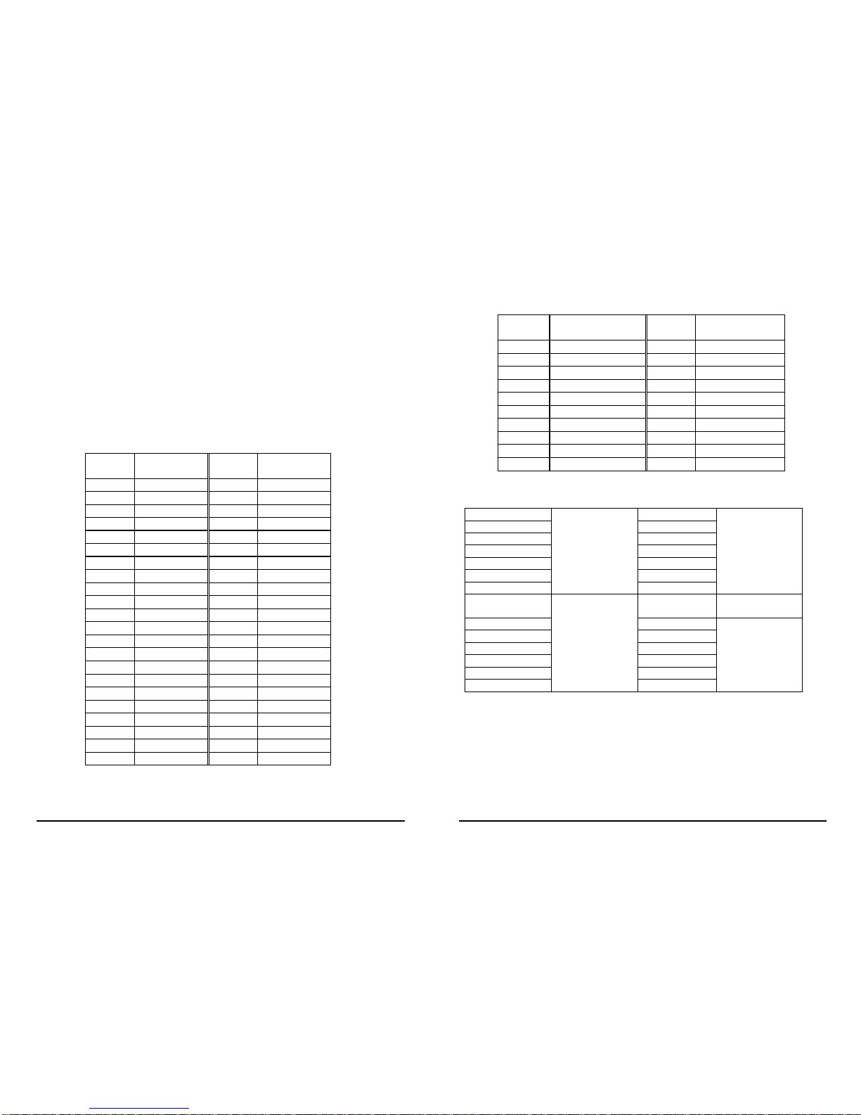
1.2 What You Have
Before you begin installing the product, please check the
following materials are included in the package:
• 1 Wafer-5820 All-in-one single board computer
• 1 CD disk for utility and drivers
• 1 2.5" IDE flat cable (44-pin 2.0mm pitch to 44-pin 2.54mm
pitch)
• 1 one to two 6pin mini Din connector for keyboard and
mouse
• 1 combo serial port cable (RS-232/422/485)
• 1 standard D25 connector for parallel cable
• 1 dual USB connector cable
• 1 floppy cable (for 3.5" FDD only)
• 1 audio cable sets
If any of these items are missing or damaged, contact your
distributor or sales representative immediately.

7
Installation
This chapter gives instructions about how to set up the
WAFER-5820 hardware, including directions of setting jumpers
and connecting peripherals, switches and indicators. Before
installation, please pay attention to the unpacking precautions on
the following page for safety.
2.1 Wafer-5820 Block Diagram & Board Layout
SDRAM
1 x S0-DIMM
Socket
RAM YUV Port
Por ( Video )
MediaGXTM
MMX-TMEnhanced
Processor
Serial
Packet
RGB Port
( Graphics )
MD [ 63:0 ]
Clocks
RTL-8139
10/100M
Ethornet
CX5530
I/O Companion
System
Clocks
CN5
USB
( 2 Ports )
CN17
Speakers
CD-1N
CD ROM
Audio
CN17
Micro-
phone
AC97
CODEC
AD1881
CN13
RJ45
14.31818
MHz Crystal
CN2
IDE
Devices
Award
BIOS
2Mb
DOC
Socket
WDT Super I/O
83977
Winbond
CN7
FDD
FDD
Printer
COM2
COM1
JP11
JP13
RS-232/
422/485
Selector
MAX
3243
CN1
Printer
COM1
RS-232
CN8
MAX
3243
LTC1487
Selftuner
intelligent
directing
Control
CN9
RS-422
RS-485
CN9
RS-232
CN4
VGA
CRT
18 bit
LVDS
CN15
CN16
Graphics Data
Analog Rgb
Video Data
IDE Control
TFT Panel
ISA Bus
Wafer-5820 Block diagram
PCI Bus
2
8
Wafer-5820 Board Layout
2
CN6
KB/MS
CN9
COM2
CN8
COM1
CN9 1
1
2
1
D6
LAN
LED
CN13
LAN
CN13
1
JP9
JP13
CN8
1
7
46
82
CN11
IR
Connector
JP10
CN11
DOC
PC104
CN10
JP11
JP121
1
GXLV
CN7
FDC
1
34
33 1
2
CN7
1
CN1
Printer
1
2
CN16
LVDS
CN4
SVGA
BIOS
CN6
5 3
1
CN4
2
1
2
1
JP8
JP7
5
19
11
6
20
1
CN16
D1
Power/HDD
LED
JP4
Reset
43
JP4
D1
JP1
CN15
CN15
LCD
CN2
2
1
44
1
CX5530
WAFER-5820
VER:2.0
U3
43
44
1
2
CN2
HDD
FAN1
1
CN3
1
CN3
Power
Connector
CN5
USB
CN5
114
CN1
2
1
CN17
Audio
CN17 2
1
CD-IN
CD-IN
1

9
2.2 Unpacking Precautions
Some components of WAFER-5820 SBC are very sensitive to
static electric charges and can be damaged by a sudden rush
of power. To protect it from unintended damage, be sure to
note these precautions:
Ground yourself to remove any static charge before touching
the Wafer-5820 SBC. You can do it by using a grounded wrist
strap at all times or by frequently touching any conducting
materials that is connected to the ground.
Handle your Wafer-5820 SBC by its edges. Don’t touch IC
chips, leads or circuitry if not necessary.
Do not plug any connector or jumper while the power is on.
2.3 System Memory DRAM
There is one 144-pin SO-DIMM socket to accept 3.3V
non-buffered SDRAM. The max. Memory size is 128MB.
2.4 Watch-Dog Timer Setting
The Watch-Dog Timer is enabled by reading port 443H. It
should be triggered before the time-out period ends, otherwise
it will assume the program operation is abnormal and will issue
a reset signal to start again, or activate NMI to CPU. The
Watch-Dog Timer is disabled by reading port 043/843H.detail
information on Watch-Dog Timer Refer to Appendix A
•JP10 : Watch-Dog Active Type Setting
JP10 DESCRIPTION
1-2ACTIVATE NMI TO CPU WHEN WDT
TIME-OUT
2-3RESET WHEN WDT TIME-OUT
OPEN DISABLE WDT
10
2.5Clear CMOS Setup
If you need to clear the CMOS Setup (for example forgot the
password you should clear the setup and then set the
password again.), you should close the JP9 about 3 seconds,
then open it again. Set back to normal operation mode, open
JP9.
•JP9: Clear CMOS Setup (Reserve Function)
JP9 DESCRIPTION
1-2Normal Operation
2-3Clear CMOS Setup
2.6 COM2 Setting JP12 , JP13
The COM2 (CN9) can supply +5V or +12V power to the serial
devices via RI pin (Pin 8) of the COM port connector. The max.
current is 1A with fuse protection, from these two connector’s
5V/12V output. If the output is set to 12V, make sure that you
have 12V to supply to the board.
CN9 Pin 8 JP13 JP12
RI Signal 2-3Don’t care
+5V 1-22-3
+12V 1-21-2
COM2 RS-232, RS-422 or RS-485 Setting JP11
The COM2 (CN9) can be set to RS-232 or RS-422/485 for
industrial field site application. Moreover when this port set to
the RS-485 mode the board equipped self-tuner IC will
automatic sensing the data direction to eliminate the data
collision. This is especially important in WINDOWS
programming which do not allow the program to catch the
control pin at your wish.

11
JP11 DESCRIPTION
1-2RS232
2-3RS422/RS485
2.7 LCD Vcc Voltage Selector
The LCD interface connector CN15 can provide 5V or 3.3V
power supply by selecting the JP1 to meet the different LCD
requirement.
JP1 DESCRIPTION
1-25V
2-33.3V
2.8 DiskOnChip™ Flash Disk Memory Address setting
The DiskOnChip™ Flash Disk Chip (DOC) is produced by
M-Systems. Because the DOC is 100% compatible to hard disk
and DOS Customer don‘t need any extra software utility. It is
just “plug and play”, easy and reliable. Right now the DOC is
available from 2MB to 144MB.The MD-2200-Xmb series DOC
will share only 8KB memory address.
•JP7 & JP8: DiskOnChip Memory Address Setting
JP8 JP7
ADDRES
1-23-45-67-81-23-45-6
CC000 OPEN
OPEN
CLOSE
OPEN
OPEN
CLOSE
CLOSE
CE000 OPEN
OPEN
OPEN
CLOSE
OPEN
CLOSE
CLOSE
D0000 CLOSE
OPEN
OPEN
OPEN
CLOSE
OPEN
CLOSE
D2000 OPEN
CLOSE
OPEN
OPEN
CLOSE
OPEN
CLOSE
D4000 OPEN
OPEN
CLOSE
OPEN
CLOSE
OPEN
CLOSE
D6000 OPEN
OPEN
OPEN
CLOSE
CLOSE
OPEN
CLOSE
D8000 CLOSE
OPEN
OPEN
OPEN
OPEN
OPEN
CLOSE
DA000 OPEN
CLOSE
OPEN
OPEN
OPEN
OPEN
CLOSE
DC000 OPEN
OPEN
CLOSE
OPEN
OPEN
OPEN
CLOSE
DE000 OPEN
OPEN
OPEN
CLOSE
OPEN
OPEN
CLOSE
12
Connection
This chapter describes how to connect peripherals, switches
and indicators to the WAFER-5820 board.
3.1 Floppy Disk Drive Connector (CN7)
WAFER-5820 board is equipped with a 34-pin daisy-chain
driver connector cable.
CN7: FDC CONNECTOR
PIN NO.
DESCRIPTION
PIN NO.
DESCRIPTION
1GROUND 2REDUCE WRITE
3GROUND 4N/C
5GROUND 6N/C
7GROUND 8INDEX#
9GROUND 10 MOTOR ENABLE A#
11 GROUND 12 DRIVE SELECT B#
13 GROUND 14 DRIVE SELECT A#
15 GROUND 16 MOTOR ENABLE B#
17 GROUND 18 DIRECTION#
19 GROUND 20 STEP#
21 GROUND 22 WRITE DATA#
23 GROUND 24 WRITE GATE#
25 GROUND 26 TRACK 0#
27 GROUND 28 WRITE PROTECT#
29 GROUND 30 READ DATA#
31 GROUND 32 SIDE 1 SELECT#
33 GROUND 34 DISK CHANGE#
3

13
3.2 PCI E-IDE Disk Drive Connector (CN2)
For IDE HDD connection, The Wafer-5820 was designed with
one 2.0mm connector (CN2), which could be converted to two
2.54mm standard IDE connector via proprietary cable. Using
this cable you can attach two IDE hard disk drives to the
WAFER-5820.
CN2 : 44-pin Primary Mini-pitched IDE Interface Connector
•CN2 : Primary IDE Interface Connector
PIN NO. DESCRIPTION
PIN NO. DESCRIPTION
1RESET# 2GROUND
3DATA 7 4DATA 8
5DATA 6 6DATA 9
7DATA 5 8DATA 10
9DATA 4 10 DATA 11
11 DATA 3 12 DATA 12
13 DATA 2 14 DATA 13
15 DATA 1 16 DATA 14
17 DATA 0 18 DATA 15
19 GROUND 20 N/C
21 IDE DRQ 22 GROUND
23 IOW# 24 GROUND
25 IOR# 26 GROUND
27 IDE CHRDY 28 GROUND
29 IDE DACK 30 GROUND–DEFAULT
31 INTERRUPT 32 N/C
33 SA1 34 N/C
35 SA0 36 SA2
37 HDC CS0# 38 HDC CS1#
39 HDD ACTIVE# 40 GROUND
41 VCC 42 GROUND
43 GROUND 44 GROUND
14
3.3 Parallel Port (CN1)
This port is usually connected to a printer, The WAFER-5820
includes an on-board parallel port(CN1), accessed through a
26-pin flat-cable connector .
•CN1: Parallel Port Connector
PIN NO.
DESCRIPTION PIN NO.
DESCRIPTION
1STROBE# 2DATA 0
3DATA 1 4DATA 2
5DATA 3 6DATA 4
7DATA 5 8DATA 6
9DATA 7 10 ACKNOWLEDGE
11 BUSY 12 PAPER EMPTY
13 PRINTER SELECT 14 AUTO FORM FEED #
15 ERROR# 16 INITIALIZE
17 PRINTER SELECT LN#
18 GROUND
19 GROUND 20 GROUND
21 GROUND 22 GROUND
23 GROUND 24 GROUND
25 GROUND 26 N/C
3.4 Series Ports (CN8, CN9)
The Wafer-5820 offers two high speeds NS16C550 compatible
UARTs with Read/Receive 16 byte FIFO serial ports. These
ports let you connect to serial devices or a communication
network. One 9-pin D-SUB connector and one 14-pin header
are provided by the WAFER-5820. The detailed pin
assignment of the connectors are specified as following tables:

15
•CN8: Serial Port1 Connector (9-pin DSUB)
PIN NO.
DESCRIPTION
1DATA CARRIER DETECT (DCD)
2RECEIVE DATA (RXD)
3TRANSMIT DATA (TXD)
4DATA TERMINAL READY (DTR)
5
GROUND (GND)
6DATA SET READY (DSR)
7REQUEST TO SEND (RTS)
8CLEAR TO SEND (CTS)
9RING INDICATOR (RI)
•CN9: Serial Port2 Connector (14-pin Header/W Housing)
PIN NO.
DESCRIPTION
PIN NO.
DESCRIPTION
1DCD 2DSR
3RX 4RTS
5TX 6CTS
7DTR 8RI
9GND 10 N/C
11 TX2+ 12 TX2-
13 RX2+ 14 RX2-
RS-232
RS-422/485
1
LITHIUM
3V
+ +
+
RS-232RS-422/485
1
CN9
123
4
5
678
9
TX2-TX2+
RX2+
RX2-
RS-422/485
16
Note : TX2+,TX2-and RX2+,RX2-are for transmitting and
receiving, respectively, in the RS-422 connection. While in
RS-485 connection, TX2+,RX2+ and TX2-,RX2-must be
twisted each. Anyhow, you can only choose to use
RS-232 or RS-422/485.
3.5 Audio Connector
The audio function was organized by CX5530 I/O companions
and NS AD1881 CODEC, which compliant with AC97. You
can use CD-IN as the input port (e.g.: connected to the output
of CD player), depending on the type of connector that you
have.
•CD-IN : CD_AUDIO INPUT Connector
PIN NO.
DESCRIPTION
1JCD_R
2GND
3JCD_L
4GND
•CN17: Audio Connector
This is the output port of your Sound System. Pin 1-2-3 can be
connected to earphone and 5-6-7 can be connected to loudspeaker.
Pin 9-10-11 can be used as input port if it is connected to the
earphone jack of your CD. Pin 15-16 is for microphone.
PIN NO.
DESCRIPTION PIN NO.
DESCRIPTION
1LINE OUT L 2GND
3LINE OUT R 4GND
5LINE OUT R 6LINE OUT L
7GND 8GND
9LINE IN R 10 LINE IN L
11 GND 12 GND
13 N/C 14 N/C
15 MIC IN 16 GND

17
3.6 Keyboard & PS/2 Mouse Connector (CN6)
A 6-pin mini DIN connector (CN6) is located on the mounting
bracket for easy connection to a keyboard or PS/2 mouse. The
card comes with a cable to convert from the 6-pin mini-DIN
connector to two 6-pin mini-DIN connector for keyboard and
mouse connection
•CN6: 6-pin Mini-DIN Keyboard & Mouse Connector
PIN NO.
DESCRIPTION
1KEYBOARD DATA
2MOUSE DATA
3GROUND
4+5V
5KEYBOARD CLOCK
6MOUSE CLOCK
3.7 USB Port Connector CN5
The WAFER-5820 provides two USB interfaces, which gives
the completed plug and play, for up to 127 external devices.
•CN5: Internal USB Connector
1. USBVCC1 2. D1F-
3. D1F+ 4. GND
5. USBVCC2 6. D2F-
7. D2F+ 8. GND
9. GND 10. GND
3.8 IrDA Infrared Interface Port (CN11)
The WAFER-5820 built-in a IrDA port which support Serial
Infrared (SIR) or Amplitude Shift Keyed IR(ASKIR) interface.
When use the IrDA port have to set SIR or ASKIR model in the
BIOS’s Peripheral Setup’s COM2. Then the normal RS -232
COM2 will be disabled.
18
•CN11: IrDA connector
PIN NO.
DESCRIPTION
1VCC
2FIRRX
3IRRX
4Ground
5IR-TX
6CIR
3.9 VGA Connector (CN4)
The WAFER-5820 built-in 15-pin VGA connector accepts the
CRT monitor.
•CN4: 15-pin Female Connector
1RED 2GREEN
3BLUE 4NC
5GROUND 6GROUND
7GROUND 8GROUND
9NC 10 GROUND
11 NC 12 DDC DAT
13 HSYNC 14 VSYNC
15 DDCCLK
3.10 LCD/LVDS Interface Connector
The WAFER-5820 provides a 2x22-pin connector for the LCD
flat panel interface and a 2x10-pin connector for the LVDS flat
panel interface.
The Wafer 5820 comes to support TFT LCD panels at
following display options : (This is a reference table only , may
support more type panels)
Video Display type Resolution Example
TFT VGA 640X480 , 64K Color , 18bits
Toshiba LTM10C209A
TFT SVGA 800X600 , 64K Color , 18bits
Toshiba LTM12C275A

19
The TTL signal connecting interfaces located on CN15 while
LVDS on CN16.
The display options need to be setup manually from BIOS.
The BIOS “Integrated Peripheral” Setup will allow you to
choose display resolution either 640X480 or 800X600.
•CN15: LCD Interface Connector –only support up to 24 bit LCD.
For better display quality, the length of LCD cable should
be shorter than 35 cm.
PIN
NO. Description PIN
NO. Description
1+12V 2+12V
3GND 4GND
5+5V 6+5V
7FPVEE 8GND
9P0 10 P1
11 P2 12 P3
13 P4 14 P5
15 P6 16 P7
17 P8 18 P9
19 P10 20 P11
21 P12 22 P13
23 P14 24 P15
25 P16 26 P17
27 P18 28 P19
29 P20 30 P21
31 P22 32 P23
33 GND 34 GND
35 SHFCLK 36 FLM
37 M38 LP
39 GND 40 ENABLK
41 GND 42 N/C
43 +5V 44 5V
20
•
CN16: LVDS Interface Connector
PIN NO.
Description PIN
NO. Description
1PCLD(5V/12V) 2PCLD(5V/12V)
3GND 4GND
5TxOUT0A-6TxOUT0A+
7GND 8TxOUT1A-
9TxOUT1A+ 10 GND
11 TxOUT2A-12 TxOUT2A+
13 GND 14 TxCLKOUTA-
15 TxCLKOUTA+ 16 GND
17 FPENABKL 18 FPENAVDD
19 GND 20 GND
¡E
LVDS Signal Description—only support up to 18-bit LCD.
P18 (R0)P4 (B2)
P19 (R1)P5 (B3)
P20 (R2)P6 (B4)
P21 (R3)P7 (B5)
P22 (R4)LP
P23 (R5)FLM
P10 (G0)
TxOUT0A-
TxOUT0A+
M
TxOUT2A-
TxOUT2A+
P11 (G1)SHFCLK TxCLKOUTA-
TxCLKOUTA-
P12 (G2)
P13 (G3)
P14 (G4)
P15 (G5)
P2 (B0)
P3 (B1)
TxOUT1A-
TxOUT1A+
3.11 LAN RJ45 Connector
The WAFER-5820 built-in RJ45 LAN connector is for
10/100Mbps Ethernet (RTL8139B).

21
•CN13: LAN RJ45 Connector
1TX+ 5NC
2TX-6RX-
3RX+ 7NC
4NC 8NC
3.12 Fan Connector (FAN1)
The WAFER-5820 provides CPU cooling fan connector FAN1
that can supply 12V & 5V. to the cooling fan.
•FAN1: Fan Connector
PIN
NO. DESCRIPTION
1VCC5V
2. Ground
3. 12V
3.13 External Power Connector
The WAFER-5820 has an on-board external power connector
CN3. You can connect power directly to the CPU board.
•CN3: External Power Connector
PIN
NO. DESCRIPTION
1+12V
2GROUND
3GROUND
4VCC5V
3.14 PC/104 Connection Bus
The WAFER-5820 PC/104 expansion bus let you attach any
kind of PC/104 modules. The PC/104 bus has already
become the industrial embedded PC bus standard, so you
can easily install over thousands of PC/104 modules from
hundreds of vendors in the world. There are two PC/104
connectors on this board: PC/104-64 and PC/104-40.
22
•
CN12: PC/104-40 Connector
PIN NO.
Description PIN NO
Description
1GND 21 GND
2SBHE# 22 MCS16#
3LA23 23 IOCS16#
4LA22 24 IRQ10
5LA21 25 IRQ11
6LA20 26 IRQ12
7LA19 27 IRQ15
8LA18 28 IRQ14
9AL17 29 DACK0#
10 MEMR# 30 DRQ0
11 MEMW# 31 DACK5#
12 SD8 32 DRQ5
13 SD9 33 DACK6#
14 SD10 34 DRQ6
15 SD11 35 DACK7#
16 SD12 36 DRQ7
17 SD13 37 VCC
18 SD14 38 MASTER#
19 SD15 39 GND
20 GND 40 GND

23
•CN10: PC/104-64 Connector
PIN NO.
Description PIN NO.
Description
1IOCHCK# 33 GND
2SD7 34 IRSTDRV
3SD6 35 VCC
4SD5 36 IRQ9
5SD4 37 -5V
6SD3 38 N/C
7SD2 39 -12V
8SD1 40 ZWS
9SD0 41 +12V
10 IOCHRDY 42 GND
11 AEN 43 SMEMW#
12 LA19 44 SMEMR#
13 LA18 45 IOW#
14 LA17 46 IOR#
15 SA16 47 DACK3#
16 SA15 48 DRQ3
17 SA14 49 DACK1#
18 SA13 50 DRQ1
19 SA12 51 REFRESH#
20 SA11 52 SYSCLK
21 SA10 53 IRQ7
22 SA9 54 N/C
23 SA8 55 IRQ5
24 SA7 56 IRQ4
25 SA6 57 IRQ3
26 SA5 58 N/C
27 SA4 59 TC
28 SA3 60 BALE
29 SA2 61 VCC
30 SA1 62 OSC
31 SA0 63 GND
32 GND 64 GND
24
3.15 Ethernet LED and Power/HDD LEDS
D6:Ethernet LED setup
LED Setting
Green lamp Rx
Orange lamp
Tx
D1:Power/HDD setup
LED Setting
Green lamp Power
Orange lamp
HDD

25
AWARD BIOS Setup
WAFER-5820 uses the AWARD PCI/ISA BIOS for system
configuration. The AWARD BIOS setup program is designed to
provide maximum flexibility in configuring the system by offering
various options which may be selected to meet end-user
requirements. This chapter is written to assist you in the proper
usage of these features.
4.1 Getting Start
When you turn on the power button, the BIOS will enter the
Power-On-Self-Test routines. These routines will be executed for
system test and initialization and system configuration verification.
After the POST routines are completed, the following message
appears :
" Hit DEL if you want to run SETUP"
To access AWARD BIOS SETUP UTILITY, press <Del> key.
The following screen will be displayed at this time:
4
26
4.2 Standard CMOS Setup
The Standard CMOS Setup is used for basic hardware system
configuration. The main function is for Date/Time setting and
Floppy/Hard Disk Drive setting. Please refer the following
screen for this setup.
To set the Date, for example, press either the arrow or <Enter> button on
your keyboard to select one of the fields (Month, Date or Year) then press
either <PgUp> or <PgDn> to increase or decrease the value of that field. Do
the same steps for Time setting.
For IDE hard disk drive setup, please check the following possible setup
procedure:
1.Use the Auto setting for detection during boot-up.
2.Use the IDE HDD AUTO DETECTION in the main menu,
the computer will automatically detect the HDD
specifications.

27
3.Manually enter the specifications by yourself from
the ”User“ option.
Note:
If you need more information on any particular field, just highlight it then press <F1>
button. A pop-up windows will come out to give you more information on that field.
4.3 BIOS Features Setup
This BIOS Features Setup is designed for the 'fine tuning' of
your system in order to improve its performance. As for normal
operation, you don‘t have to change any default setting. The
default setting is pre-set for most reliable operation.
28
4.4 Chipset Features Setup
This setup function works mostly on board's chipset. This
option is used to change the chipset's configuration. Please,
carefully change any default setting, otherwise the system will
run unstable.

29
4.5 Power Management Setup
Power Management Setup helps user to handle the
ROCKY-568SEV board‘s “green” function. This feature can
shut down the video display and hard disk to save energy, for
example. The power management setup screen is as following
30
4.6 PNP / PCI CONFIGURATION
This menu is used to assign certain IRQ to your PNP/PCI
devices manually.
PNP OS Installed: if you install Plug and Play operating
system (OS), the OS will reassign the interrupt if you select Yes
in this field. If you install a non-Plug and Play OS or if you want
to prevent reassigning of interrupt settings, select No in this
field.
Resources Controlled By: select Auto if you want the
computer to assign the IRQs automatically and vice versa.
Reset Configuration Data: Enabling this field means you
allow the configuration data to be reset.
IRQ-xx assigned to: these fields show whether certain IRQ is
used by a PCI/ISA card.

31
4.7 LOAD BIOS DEFAULTS
If you select 'Y' to this field, the BIOS Defaults will be loaded
except Standard CMOS SETUP. The default settings are not
optimal and turning all high performance into disable condition.
Select 'N' to abort.
Suggestion: for the first time or for our primary user, we suggest you to use
LOAD SETUP DEFAULTS because it is the most safe mode for your
system.
32
4.8 LOAD SETUP DEFAULTS
If you select 'Y' to this field, the Setup Defaults will be loaded
except Standard CMOS SETUP. The default settings are
optimal configuration settings for your system.

33
4.9 INTEGRATED PERIPHERALS
This option is used to assign Onboard I/O, IRQ, DMA etc. If
you don't know how to configure them, just press <F7> to load
Setup Defaults.
The flat panels will then be applied with two modes: 640x480 or
800x600, for which it need to set up from BIOS for proper flat
panel resolution.
lBuild in CPU Audio -- Enabled, Disabled
To disable or enable the audio function.
lAudio I/O Base Address -- 220H, 240H, 260H, 280H
To select the I/O address for audio function.
lMPU-401 I/O Base Address -- 300H, 330H, Disabled
To select the I/O address for MPU-401 (midi interface).
lAudio IRQ Select -- 5, 7, 10, Disabled
To select the interrupt for audio function.
lAudio Low DMA Select -- DMA0, DMA1, DMA3, Disabled
To select the high DMA channel.
34
lAudio High DMA Select -- DMA5, DMA6, DMA7, Disabled
To select the high DMA channel.
lMultiple Monitor Support -- No Onboard, PCI first, M/B first
To select the primary VGA for multiple monitor support in WINDOWS.
lVideo Memory Size -- 1.5M, 2.5M, 4.0M
To select the size of video memory. It makes use of system memory for
display.
4.10 SUPERVISOR PASSWORD AND USER PASSWORD
Supervisor Password sets a password that is used to protect
your system and Setup Utility. Supervisor Password has
higher priority than User Password. Once you setup the
password, the system will always ask you to key-in password
every time you enter the BIOS SETUP. If you enter the BIOS
SETUP with Supervisor Password, you can choose every
setup/option on the main menu but with User Password, you
can only choose three setup/options (USER PASSWORD,
SAVE & EXIT SETUP and EXIT WITHOUT SAVING). To
disable these passwords, enter the BIOS SETUP room with
Supervisor Password and then just press the <Enter> key
instead of entering a new password when the 'Enter
Password' prompt pop-up.
N.B. : if you forget the password, do the Clear/Reset CMOS procedure (see
Section 2.5 Clear CMOS Setup)

35
4.11 IDE HDD AUTODETECTION
This option detects the parameters of an IDE hard disk drive
(HDD sector, cylinder, head, etc) automatically and will put the
parameters into the Standard CMOS Setup screen. Up to 2
IDE drives can be detected and the parameters will be listed
in the box. Press <Y> if you accept these parameters. Press
<N> to skip the next IDE drives.
Note: If your IDE HDD was formatted in previous older system, incorrect
parameters may be detected. In this case, you need to enter the correct
parameters manually or low-level format the disk
SAVE AND EXIT SETUP
Select this option when you finish setting all the parameters and
want to save them into the CMOS. Just simply press <Enter> key
and all the configuration changes will be saved
36
Quick Without Saving
Select this option if you want to exit the Setup without saving
the changes that you made. Just simply press <Enter> key
and you will exit the BIOS SETUP without saving the changes.

37
SVGA Setup
5.1 Introduction
The WAFER-5820 is equipped with on-board LCD/VGA
interface. The description below is its specifications and features:
5.1.1 Chipset
The WAFER-5820 uses a Cyrix CX5530 chipset as its
SVGA controller. It is compatible with many common 18-bit
LCD displays and traditional analog CRT monitors. The VGA
BIOS supports LCD. Besides, it also accepts interlaced and
non-interlaced analog monitors (color and monochrome
VGA) with high-resolution quality while maintaining complete
IBM VGA compatibility. But digital monitors (i.e. MDA, CGA,
and EGA) can be NOT supported. Multiple frequency
(multisync) monitors are operated as if they were analog
monitors.
5.1.2 Display memory
Having 1.5 ~ 4 MB UMA memory, the VGA controller can
make CRT displays or color panel displays perform with
resolutions up to 1024 x 768 at 64 K colors. The display
memory can be modified up to 4 MB in BIOS for true-color
resolution of 1024 x 768.
5
38
5.1.3 Display drivers
1.Win95,98 drivers(VGA & Audio) in
Wafer-5820CD \ Geodevga95,98 \National geode Win9x
Drivers1.2.exe
2.WinNT4.0 drivers in
Wafer-5820CD\Nt40Vga\
5.2 Further Information
For more detailed information about the PCI/SVGA installation
in your WAFER-5820, including driver updates, troubleshooting
instructions, please refer to the following webs which provide some
resources you may need. If not find the information you need,
please contact with your local distributer.

39
Audio
6.1 Introduction
With on-board audio interface, the WAFER-5820 can perform
high-quality stereo sound and FM music synthesis (ESFM) by
using the CX5530 audio controller. The audio interface has
functions of recording, compressing, and playing back voice, sound,
and music with a built-in mixer control. In addition, the on board
audio interface supports the Plug and Play (PnP) standard and
provides PnP configuration for audio, FM, and MPU-104 logical
devices. It is compatible with AC97 version 2.0, voice, and music
functions. The ESFM synthesizer is register compatible with the
OPL3 and has extended capabilities.
6.1.1 Audio drivers
1. Installing software driver in Windows NT
The driver was provided from the CD utility.
WinNT4.0 Audio drivers in
Wafer-5820CD\Audio\
2. Installing software driver in Win95/98
The software drivers was supported from Windows 95/98,
please set up from......
Win98\drivers\audio\cyrix\mgxsb16.inf
6
40
PCI Bus Ethernet Interface
7.1 Introduction
The WAFER-5820 provides a high performance 32-bit Ethernet
chipset which is completely compliant with IEEE 802.3 100 Mbps
CSMA/CD standards. It is both 100Base-T and 10Base-T
compatible. The major network operating system fits it. The
medium type can be set up via the RSET8139.exe program
included on the utility CD.
The Ethernet port supplies a standard RJ-45 connector on
board. To utilize the network boot feature is by incorporating the
boot ROM image files for the appropriate network operating system.
The boot ROM BIOS files are combined with system BIOS, which
can be enabled/disabled in the BIOS setup.
The 8139x utility tools all in
WAFER-5820CD\8139x\
7
Table of contents
Other Vox Motherboard manuals