VXIS VX1828B User manual

VX1828B
VIDEO PROCESSOR FOR MIDDLE SIZE LCD PANEL
1010
1010
0101
Video
Decoder
T
imin
g
Controller
TCON
MENU
OSD
OSD
REVISION HISTORY
Revision Date Pages Description
0.1 2005.06.09 64 Initial Draft
0.2 2005.06.14 64 Update panel support
Headquarters
5F-1,No. 9, Prosperity Rd. I, Science Based
Industrial Park, Hsin-Chu 300, Taiwan, R.O.C.
Tel : 886-3-5630888
Fax: 886-3-5630889
Taipei Office
2F-1, No.233-2, Pao-Chiao Rd., Hsin-Tien,
Taipei 231, Taiwan, R.O.C.
Tel : 886-2-29100010
Fax: 886-2-29100012
VXIS Technology Corp.
http://www.vxis.com
VXIS Technology Corp., reserves the right to change or modify the information contained herein without notice.

VX1828B
Preliminary Datasheet Video Processor for Middle Size LCD Panel
P.2/P.64
V1.0 050420
Contact VXIS or visit the website to ensure the most recent revision of the document.

VX1828B
Preliminary Datasheet Video Processor for Middle Size LCD Panel
P.3/P.64
V1.0 050420
Table of Contents
1. FEATURE............................................................................................................................................5
2. GENERAL DESCRIPTION .................................................................................................................6
3. APPLICATION ....................................................................................................................................7
4. PIN CONFIGURATION .......................................................................................................................8
4.1 PINOUT DIAGRAM .......................................................................................................................8
4.2 PIN ASSIGNMENT........................................................................................................................ 9
4.3 PIN DESCRIPTION .....................................................................................................................10
4.4 PIN-TYPE DEFINITION...............................................................................................................13
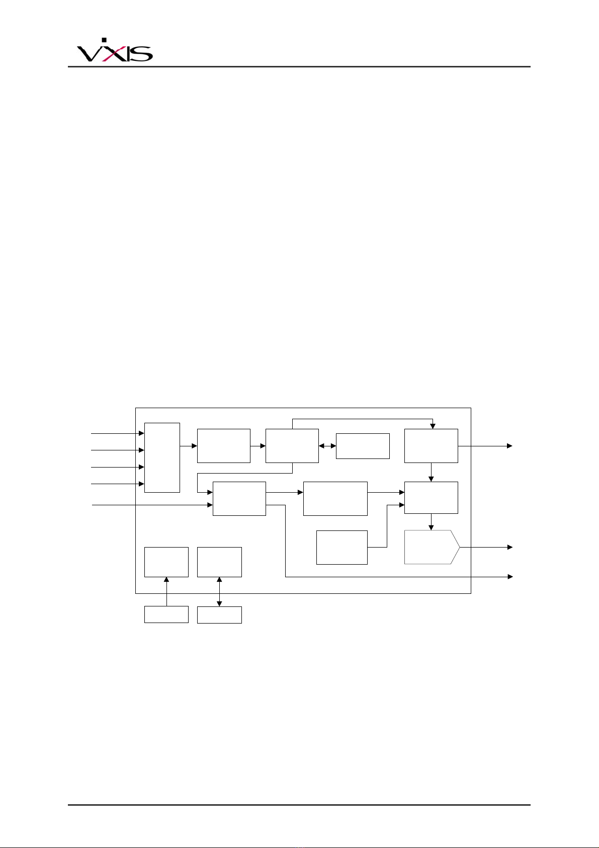
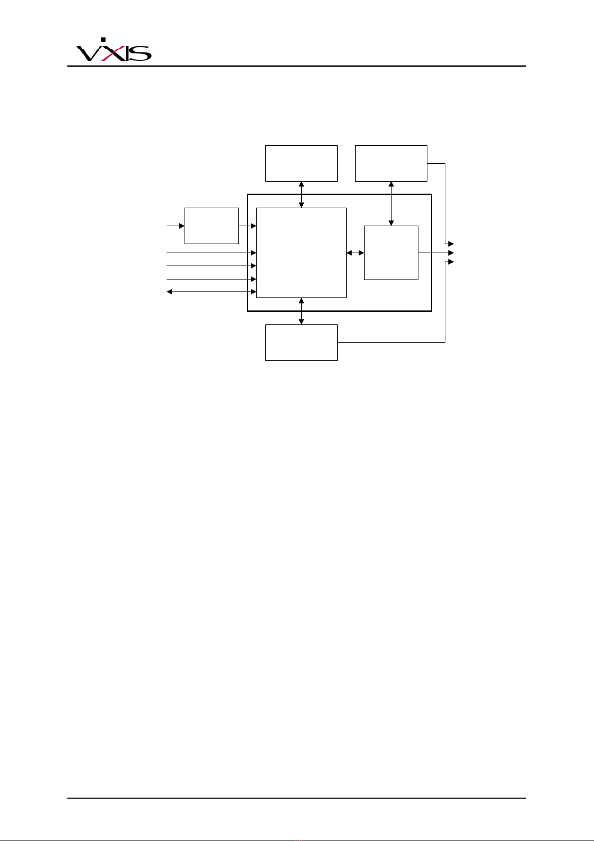
5. FUNCTION DESCRIPTION..............................................................................................................14
5.1 ANALOG INPUT CONFIGURATION ........................................................................................... 14
5.2 POWER-DOWN OPTION............................................................................................................15
5.3 MODE DETECTION....................................................................................................................15
5.4 COLOR-TRANSIENT IMPROVEMENT (CTI) .............................................................................15
5.5 LUMA/CHROMA ADJUSTMENT.................................................................................................15
5.6 TWO-DIMENSIONAL SHARPNESS ........................................................................................... 16
5.7 BLACK-LEVEL EXTENSION (BLE).............................................................................................17
5.8 INTERLACE DIGITAL INTERFACE ............................................................................................ 18
5.9 GAMMA CORRECTION ..............................................................................................................18
5.10 ON-SCREEN-DISPLAY (OSD)..................................................................................................20
5.10.1 OSD INTRODUCTIONS .....................................................................................................20
5.10.2 OSD DISPLAY BLOCKS.....................................................................................................20
5.10.3 OSD OPERATIONS............................................................................................................21
5.11 LCD TIMING CONTROLLER (T-CON)......................................................................................24
5.12 PULSE WIDTH MODULE (PWM) .............................................................................................24
6. REGISTER DESCRIPTION ..............................................................................................................25
6.1 REGISTER MAP .........................................................................................................................25
6.2 REGISTER DETAILS ..................................................................................................................29
6.2.1 Global Registers ...................................................................................................................29
6.2.2 Analog-Front-End Registers .................................................................................................31
6.2.4 Video Timing Generation Registers......................................................................................33
6.2.5 YC Separation Registers ......................................................................................................36
6.2.6 Demodulation Registers .......................................................................................................37

VX1828B
Preliminary Datasheet Video Processor for Middle Size LCD Panel
P.4/P.64
V1.0 050420
6.2.7 CCIR Registers .....................................................................................................................39
6.2.8 Picture Adjustment Registers................................................................................................42
6.2.9 Peaking and RGB-Filter Registers........................................................................................43
6.2.10 Output Format Registers ....................................................................................................44
6.2.11 OSD Registers ....................................................................................................................45
6.2.12 EZ-Gamma Programming registers....................................................................................49
6.2.13 LINE INVERSION registers ................................................................................................50
4.2.14 Timing Controller registers..................................................................................................51
6.2.15 Status registers ...................................................................................................................55
6.2.16 PWM registers ....................................................................................................................56
6.2.17 Continuous Write registers .................................................................................................57
7. ELECTRICAL CHARACTERISTICS ................................................................................................58
7.1 ABSOLUTE MAXIMUM RATINGS ..............................................................................................58
7.2 RECOMMENDED OPERATING CONDITIONS..........................................................................58
7.3 DC CHARACTERISTICS ............................................................................................................ 59
7.4 ANALOG-FRONT-END SPECIFICATION ...................................................................................60
7.5 DAC SPECIFICATION.................................................................................................................60
7.6 AC CHARACTERISTICS.............................................................................................................61
7.6.1 DIGITAL VIDEO INTERFACE............................................................................................... 61
7.6.2 HOST INTERFACE...............................................................................................................62
8. IC CONNECTION DIAGRAM ...........................................................................................................63
9. PACKAGE DIMENSION ...................................................................................................................64

VX1828B
Preliminary Datasheet Video Processor for Middle Size LCD Panel
P.5/P.64
V1.0 050420
1. FEATURE
VIDEO DECODER
Composite and S-Video Inputs: NTSC and NTSC-Japan; PAL (B, D, G, H, I, M, N, Nc)
6 Analog Inputs: Capable of 2xCVBS+2xS-Video or 4xCVBS+1xS-Video Inputs
Support CCIR656 Input/Output
Analog Automatic Gain Control
10-Bit 2-Channel A/D Converters with Fixed Sampling Clock
Require Only One Crystal (20 MHz) for All Standards
Automatic Mode Detection
Internal Phase Lock Loop to Generate Video Clock
2-D Comb Filter for Luminance and Chrominance Separation
Precise Chrominance Demodulation
Internal Buffers for Video Stability Control
Frequency Directive 2-D Sharpening
Brightness, Contrast, Color, and Tint Adjustments
Adaptive Black-Level Extension
Video Noise Reduction
Chrominance Transient Improvement
EZ-Gamma Programming Hardware Support
MacroVision Copy Right Detection
OSD
160-Character Font Memory (128 built-in plus 32 user-defined characters)
Alpha-Blending with OSD Content and Video
Blinking and Highlight Function
LCD DISPLAY CONTROL
Build-in Universal T-CON for 480/960/1200/1440/1920x234 analog LCD panels
Digital RGB Independent Output Line-Inversion, Offset, and Ratio Control
Built-In Video DAC for Analog RGB Output
INTERFACE
Two-Wire Serial Host Interface Compatible with IIC Interface
2.5/3.3V Power Supply
5-Volt Tolerant Digital I/O; Optional open-drain panel interface
100-Pin LQFP Package

VX1828B
Preliminary Datasheet Video Processor for Middle Size LCD Panel
P.6/P.64
V1.0 050420
2. GENERAL DESCRIPTION
VX1828B is a high quality video processor IC for middle size LCD panel application. VX1828B can
accept digital or analog video inputs, then output digital or analog video signals. The digital input is
CCIR656 and the analog input is NTSC/PAL video signals from TV tuner, DVD, or VCR sources,
including weak and distorted signals. VX1828B decodes these video inputs into R/G/B analog signals
or CCIR656 digital format. The R/G/B analog signals directly drive the panel with build-in timing
controller.
The build-in automatic gain control (AGC) and 10-bit 2-channel AD converters maintain high-resolution
video quality, and with automatic video mode detection, user can freely switch and adjust variety of
signal source. The multiple internal adaptive PLLs also can help precisely extract pixel clock from
video source and perform sharp-and-keen color demodulation. Adaptive 2-D comb-filter, 2-D
sharpening, and synchronization are implemented with build-in line-buffers.
The output format of VX1828B directly supports 480/960/1200/1440/1920x234 analog TFT-LCD
modules.
VX1828B
Video
MUX
2-Channel
AFE
Video
Decoder
Horizontal
Scaler
Line
Buffer
Host
Interface
2-Wire
Serial Host
Signals
HOST
3-Channel
DAC
S-Video 2
S-Video 1
CVBS 2
CBVS 1
R / G / B
Control
Signals
LCD Timing
Controller
PLL
Crystal
CCIR 656
CCIR 656
OS
OSD
Picture
Enhancement
Figure 2.1 Block Diagram

VX1828B
Preliminary Datasheet Video Processor for Middle Size LCD Panel
P.7/P.64
V1.0 050420
3. APPLICATION
Video Decoder
TV Tuner
TV / Cable Signal
DVD / VCD Signal
S-Video
Micro-
Controller
RGB
Amplifier
General
Purpose
TCON
TCON / Vcom
Application
Circuitry
to TFT-LCD
module
2-Wire Host Signal
Interface
VX1828B
CVBS
CVBS1
CVBS2
S1
S2
CCIR 656
CCIR 656

VX1828B
Preliminary Datasheet Video Processor for Middle Size LCD Panel
P.8/P.64
V1.0 050420
4. PIN CONFIGURATION
4.1 PINOUT DIAGRAM
VX1828B
25
1
2
3
4
5
6
7
8
9
10
11
12
13
14
15
16
17
18
19
20
21
22
23
24
75
51
52
53
54
55
56
57
58
59
60
61
62
63
64
65
66
67
68
69
70
71
72
73
74
26
27
28
29
30
50
49
48
47
46
45
44
43
42
41
40
39
38
37
36
35
34
33
32
31
81
82
83
84
85
86
87
88
89
90
91
92
93
94
95
96
97
98
99
100
76
77
78
79
80
/RESET
N.C.
AIY0
AIY1
AIY2
AIC0
AAFOY
AAFIY
AAFOC
AAFIC
AIY3
DVDDP5
XTALI
XTALO
DGNDP5
AVDD_AFE
AGND_AFE
AVDD_PLL1
AIC1
IR
AGND_PLL1
DGND_PLL1
DVDD_PLL1
LPFI
LPFO
SDA
SCL
N.C.
N.C.
AVDD_SHIELD
DVDDC4
OE3_CPH3
OOEH
DVDDC3
CCIR6
HSYNC
VSYNC
VOCLK
DGNDP1
DVDDP1
CCIR7
CCIR5
CCIR4
CCIR0
CCIR1
CCIR2
CCIR3
OSTH2
OSTH1
OCPH1
OCPV
OE1
OE2_CPH2
OPOLS
OSTV1
OSTV2
DGNDC3
CHSY
CVSY
CCLK
DVDD_PDA
IG
IB
AGND_SHIELD
N.C.
UD_CTRL
LR_CTRL
N.C.
DGNDP2
DVDDP2
DGNDP4
DVDDP4
DVDDC2
DGNDC2
DVDDP3
DGNDP3
DVDDC1
DGNDC1
AVDD_AD
AGND_AD
DGND_PDA
LQFP100
OQ1H
DGNDC4
VREG
AGND_BIAS1
AGND_BIAS2
DAC_RSET
AVDD_DACL
AVDD_RGB
AVDD_BIAS2
ADC_RSET
AVDD_BIAS1
AVDD_PLL2
AGND_PLL2
AGND_DACL
AGND_RGB
N.C.
N.C.
N.C.
N.C.

VX1828B
Preliminary Datasheet Video Processor for Middle Size LCD Panel
P.9/P.64
V1.0 050420
4.2 PIN ASSIGNMENT
Pin # Pin Name Pin # Pin Name Pin # Pin Name Pin # Pin Name
1 VREG 26 DVDD_PDA 51 OCPV 76 CVSY
2 DVDDP5 27 AVDD_BIAS1 52 OE3_CPH3 77 CHSY
3 DGNDP5 28 AVDD_BIAS2 53 OE2_CPH2 78 CCLK
4 XTALO 29 AGND_BIAS1 54 OE1 79 DGNDC3
5 XTALI 30 AGND_BIAS2 55 DGNDP1 80 DVDDC3
6 N.C. 31 ADC_RSET 56 DVDDP1 81 CCIR7
7 DVDD_PLL1 32 DAC_RSET 57 OOEH 82 CCIR6
8 DGND_PLL1 33 AVDD_PLL2 58 OSTH1 83 DGNDP3
9 AVDD_PLL1 34 AGND_PLL2 59 OSTH2 84 DVDDP3
10 AGND_PLL1 35 N.C. 60 DGNDC1 85 CCIR5
11 AAFIC 36 LPFI 61 DVDDC1 86 CCIR4
12 AAFOC 37 AVDD_DACL 62 OCPH1 87 CCIR3
13 AIC0 38 AGND_DACL 63 OQ1H 88 CCIR2
14 AIC1 39 LPFO 64 N.C. 89 CCIR1
15 AGND_AFE 40 AVDD_RGB 65 DGNDP2 90 CCIR0
16 AVDD_AFE 41 AGND_RGB 66 DVDDP2 91 DGNDP4
17 AIY0 42 IR 67 OPOLS 92 DVDDP4
18 AIY1 43 IG 68 VOCLK 93 SDA
19 AIY2 44 IB 69 DGNDC2 94 SCL
20 AIY3 45 AVDD_SHIELD 70 DVDDC2 95 N.C.
21 AAFOY 46 AGND_SHIELD 71 HSYNC 96 N.C.
22 AAFIY 47 N.C. 72 VSYNC 97 /RESET
23 AVDD_AD 48 N.C. 73 LR_CTRL 98 N.C.
24 AGND_AD 49 OSTV1 74 UD_CTRL 99 DGNDC4
25 DGND_PDA 50 OSTV2 75 N.C. 100 DVDDC4

VX1828B
Preliminary Datasheet Video Processor for Middle Size LCD Panel
P.10/P.64
V1.0 050420
4.3 PIN DESCRIPTION
Video Analog Input Pins (6)
Name Type Description Notes
AIY3 AI Analog Composite Input
AIY2 AI Analog Composite Input
AIY1 AI Analog Composite or Luminance Input
AIY0 AI Analog Composite or Luminance Input
AIC1 AI Analog Chrominance Input
AIC0 AI Analog Chrominance Input
Auxiliary Analog I/O Pins (8)
NAME Type Description Notes
AAFOY AO Analog Signal to Optional External Anti-Alias Filter of Y-channel
AAFOC AO Analog Signal to Optional External Anti-Alias Filter of C-channel
AAFIY AI Analog Signal from Optional External Anti-Alias Filter of Y-channel
AAFIC AI Analog Signal from Optional External Anti-Alias Filter of C-channel
LPFO AO Output to DAC Reconstruction Filter
LPFI AI Input from DAC Reconstruction Filter
ADC_RSET AI Connect to an External Resister for Setting the Bias Current of ADC
DAC_RSET AI Connect to an External Resister for Setting the Output Current of DAC
CCIR Input/Output Pins (11)
NAME Type Description Notes
CCIR0~7 I/O1CCIR656 Data Input/Output
CCLK I/O1CCIR656 Clock Input/Output
CHSY I/O1CCIR656 HSYNC Input/Output
CVSY I/O1CCIR656 VSYNC Input/Output

VX1828B
Preliminary Datasheet Video Processor for Middle Size LCD Panel
P.11/P.64
V1.0 050420
Video Output Pins (6)
Name Type Description Notes
IR AO Analog Video Output Red Note 1
IG AO Analog Video Output Green Note 1
IB AO Analog Video Output Blue Note 1
HSYNC I/O1Video Output Horizontal Synchronization Note 2
VSYNC I/O1Video Output Vertical Synchronization Note 2
VOCLK I/O2Video Output Clock Note 2
T-CON Pins (14)
Name Type Description Notes
OPOLS O1Polarity Alternating Signal for Video
OE3_CPH3 O1Output Enable Control Signal for Gate Driver / 3rd Source Driver Shift
Clock
OE2_CPH2 O1Output Enable Control Signal for Gate Driver / 2nd Source Driver Shift
Clock
OE1 O1Output Enable Control Signal for Gate Driver
OSTV2 I/O1Gate Driver Start Pulse
OSTV1 I/O1Gate Driver Start Pulse
OCPV O1Gate Driver Shift Clock
OCPH1 O1Source Driver Shift Clock
OSTH1 I/O1Source Driver Start Pulse
OSTH2 I/O1Source Driver Start Pulse
OOEH O1Output Enable Control Signal for Source Driver
OQ1H O1Analog Signal Rotate Indicator for Delta-aligned RGB Panel
UD_CTRL O1Output for LCD Panel Up/Down Switch
LR_CTRL O1Output for LCD Panel Left/Right Switch
Note 1: Order of IR, IG, and IB could be changed by programmable registers.
Note 2: HSYNC, VSYNC, VOCLK could be selected as PWM output individually.

VX1828B
Preliminary Datasheet Video Processor for Middle Size LCD Panel
P.12/P.64
V1.0 050420
Miscellaneous I/O Pins (5)
Name Type Description Notes
XTALO XO Crystal Output
XTALI XI Crystal Input
SDA I/O1Host Interface Serial Data / Address
SCL ISHost Interface Serial Clock
/RESET ISChip Reset (Active Low)
Power Pins (41)
Name Type Description Notes
DVDDC1~4 P25 Digital Supply 2.5V for Core
DVDDP1~5 P25 Digital Supply 3.3V for I/O
DVDD_PLL1 P33 Digital Supply 3.3V for PLL1
DVDD_PDA P33 Digital Supply 3.3V for PLL2, ADC, and DAC
AVDD_PLL1 P33 Analog Supply 3.3V for PLL1
AVDD_AFE P33 Analog Supply 3.3V for AFE
AVDD_AD P33 Analog Supply 3.3V for ADC
AVDD_BIAS1 P33 Analog Supply 3.3V for BIAS
AVDD_BIAS2 P33 Analog Supply 3.3V for BIAS
AVDD_PLL2 P33 Analog Supply 3.3V for PLL2
AVDD_DACL P33 Analog Supply 3.3V for PLL2 DAC
AVDD_RGB P33 Analog Supply 3.3V for RGB DAC
AVDD_SHIELD P33 Analog Supply 3.3V for Shielding
VREG P25 Regulator Output 2.5V
DGNDC1~4 G Digital Ground for Core
DGNDP1~5 G Digital Ground for I/O
DGND_PLL1 G Digital Ground for PLL1
DGND_PDA G Digital Ground for PLL2, ADC, and DAC
AGND_PLL1 G Analog Ground for PLL1
AGND_AFE G Analog Ground for Analog Front End
AGND_AD G Analog Ground for ADC
AGND_BIAS1 G Analog Ground for BIAS
AGND_BIAS2 G Analog Ground for BIAS
AGND_PLL2 G Analog Ground for PLL2
AGND_DACL G Analog Ground for PLL DAC
AGND_RGB G Analog Ground for RGB DAC

VX1828B
Preliminary Datasheet Video Processor for Middle Size LCD Panel
P.13/P.64
V1.0 050420
AGND_SHIELD G Analog Ground 3.3V for Shielding
4.4 PIN-TYPE DEFINITION
TYPE DEFINITION
I 5V Tolerant Input
IS5V Tolerant Schmitt Trigger Input
IPU 5V Tolerant Input with Internal Pull-Up Resistor
IPD 5V Tolerant Input with Internal Pull-Down Resistor
O1TTL Output Group 1 (4 mA)
OTS1 Tri-State Output Group 1 (4 mA)
I/O15V Tolerant Input/TTL Output Group 1 (4 mA)
I/O25V Tolerant Input/TTL Output Group 2 (8 mA)
XI, XO Crystal Pin
AI Analog Input Pin
AO Analog Output Pin
P Power Pin
G Ground Pin

VX1828B
Preliminary Datasheet Video Processor for Middle Size LCD Panel
P.14/P.64
V1.0 050420
5. FUNCTION DESCRIPTION
5.1 ANALOG INPUT CONFIGURATION
VX1828B has 6 analog video input pins that can be configured by the register, AISEL as follows.
Table 5.1 Analog Input Configurations
Video Source
S-Video
AISEL
CVBS
Y C
0000 AIY<0>
0001 AIY<1>
0010 AIY<2>
0011-0101 Reserved
0110 AIY<0> AIC<0>
0111 AIY<1> AIC<1>
1000-1001 Reserved
1010 AIY<3>
1011-1111 Reserved

VX1828B
Preliminary Datasheet Video Processor for Middle Size LCD Panel
P.15/P.64
V1.0 050420
5.2 POWER-DOWN OPTION
In CCIR input mode, the VX1828B provides the option to power down the line-lock sampling and
demodulation circuits.
5.3 MODE DETECTION
Automatic video mode detection is built in, discriminating between NTSC, PAL-M, PAL-Nc and other
PAL formats. Manual override of automatic mode detection is available that is controlled by the ML525
(NTSC and PALM) and MVSTD (NTSC and other PAL) registers.
Table 5.2 Manual Mode Settings
ML525 MVSTD Mode
0 0 PAL (Combination N)
0 1 PAL (B,D,G,H,I,N)
1 0 PAL (M)
1 1 NTSC
5.4 COLOR-TRANSIENT IMPROVEMENT (CTI)
The color-transient improvement (CTI) engine in VX1828B works adaptively to sharpen the transition
of chrominance edges to perform sharp and keen edges for every objects and overall clearer video to
the viewers.
5.5 LUMA/CHROMA ADJUSTMENT
Contrast is adjusted by register CONTRAST. This provides a range of gain from zero up to 255/128 -
almost 2X. A value of CONTRAST = 128 provides a gain of 1.
Brightness is adjusted by register BRIGHTNESS. This provides an adjustment of +127 to -128 to luma
which is clipped if necessary to achieve the required range of 64 to 940.
Hue is adjusted by register HUE. The value of HUE is added as a color phase adjustment.
Saturation is adjusted by register SATURATION. The color components are multiplied by

VX1828B
Preliminary Datasheet Video Processor for Middle Size LCD Panel
P.16/P.64
V1.0 050420
SATURATION, the result is divided by 128. This provides a range of gain from zero up to 255/128 -
almost 2X. A value of SATURATION = 128 provides a gain of 1.
5.6 TWO-DIMENSIONAL SHARPNESS
The VX1828B offers three peaking filters for different frequency response in horizontal sharpness
engine. The gain for each filter is adjustable from 0 to 14 dB and individually controlled with registers,
PEAK_ADJ1, PEAK_ADJ2, and PEAK_ADJ3 (Figure 5.1). The clipping filter is adjustable with the
registers PEAK_CLIP_MIN and PEAK_CLIP_MAX.
Clipping Filter
PEAK_CLIP_MIN
PEAK_CLIP_MAX
Video Input
Video
Output
Peaking Filter 1
(High-Band
Enhancement)
Peaking Filter 2
(Mid-Band
Enhancement)
Peaking Filter 3
(Low-Band
Enhancement)
PEK_ADJ1
PEAK_ADJ2
PEAK_ADJ3
Figure 5.1 VX1828B Horizontal Sharpness Engine

VX1828B
Preliminary Datasheet Video Processor for Middle Size LCD Panel
P.17/P.64
V1.0 050420
5.7 BLACK-LEVEL EXTENSION (BLE)
Basic idea of black level extension is to enhance the contrast of the luminance in the dark potion of the
picture. The advantage of this function is to make the object more solid, apparent, and noticeable to
the viewers. The BLE function works adaptively, depending on the average luminance of the picture.
The Luminance transform function for BLE is controlled by three parameters, BKXLVL, BKXMAX, and
BKXSLP (Figure 5.2).
Input
Luminance
Output Luminance
BKXMAX - The Maximum
Location for Adaptive
Turnaround Point
BKXSLP - The Slope of The
Transform Function in BLE
Section
Linear SectionBlack Section BLE
Section
Adaptive
Turnaround Point
Depending on
Video Content
Figure 5.2 BLE Transform Function

VX1828B
Preliminary Datasheet Video Processor for Middle Size LCD Panel
P.18/P.64
V1.0 050420
5.8 INTERLACE DIGITAL INTERFACE
VX1828B supports either CCIR656 input or output. The CCIR656 data stream includes a 4:2:2 YCbCr
data multiplexed into an 8-bit stream: Cb0Y0Cr0Y1Cb2Y2Cr2, etc. Following figures illustrate the format
for 525/60 and 625/50 video systems, respectively.
F
F
0
0
0
0
X
0
8
0
1
0
8
0
1
0
8
0
1
0
F
F
0
0
0
0
X
0
C
BYC
RYC
BYC
RYF
F
EAV CODE SAV CODE
BLANKING
4268 41440
1716
START OF DIGITAL LINE
START OF ACTIVE DIGITAL LINE
HSYNC SIGNAL NEXT
LINE
CCIR 656 8-bit parallel interface data format for 525/60 video systems
F
F
0
0
0
0
X
0
8
0
1
0
8
0
1
0
8
0
1
0
F
F
0
0
0
0
X
0
C
BYC
RYC
BYC
RYF
F
EAV CODE SAV CODE
BLANKING
4280 41440
1728
START OF DIGITAL LINE
START OF ACTIVE DIGITAL LINE
HSYNC SIGNAL NEXT
LINE
CCIR 656 8-bit parallel interface data format for 625/50 video systems
The X symbol in EAV and SAV is used to indicate field and H-sync information by the rules as follows:
Even field Odd field
EAV SAV EAV SAV
X[3:0] 1101 1100 1001 1000
5.9 GAMMA CORRECTION
The VX1828B provides an alternative way to perform video transform effect with an easier approach,

VX1828B
Preliminary Datasheet Video Processor for Middle Size LCD Panel
P.19/P.64
V1.0 050420
called EZ-Gamma configuration. Built-in the registers, 33 tapes of intermediate points form the
approximate curve for basic video transformation process such as Gamma correction, or
room-temperature compensation (Figure 5.3). Each intermediate point is programmable in the register
map, from register CLUTABLE00 to register CLUTABLE32. Shown in the figure, these 33 tapes of
points conform to build a piecewise linear curve where the points between the intermediate points are
calculated from linear interpolation.
08 16 24 32 40 48 232 240 248 256
Input Luminance
Output Luminance
CLUTABLE03
CLUTABLE02
CLUTABLE32
CLUTABLE31
CLUTABLE30
CLUTABLE29
CLUTABLE06
CLUTABLE05
CLUTABLE04
CLUTABLE01
CLUTABLE00
Figure 5.3 EZ-Gamma Transform Curve
For some specific users that the Gamma correction is the most concern, the VX1828B provides an
easiest way to program and modify Gamma correction. If the register CLUTABLE_PGR[4] is set to
zero, above 33-tape piecewise linear curve is applied. If the register CLUTABLE_PGR[4] is set to one,
a set of build-in table with Gamma correction from 0.75 to 1.9 and 3 sets for specific LCD panel
correction, and can be selected by the register CLUTABLE_PGR[3:0]. For details refer to Table 5.3.

VX1828B
Preliminary Datasheet Video Processor for Middle Size LCD Panel
P.20/P.64
V1.0 050420
Table 5.3 EZ-Gamma Configurations
CLUTABLE_PGR Function CLUTABLE_PGR Function
00h-0Fh Using user-programmed
table 7Bh – 9Bh 18h (default) Gamma = 1.4
10h Gamma = 0.75 19h Gamma = 1.5
11h Gamma = 0.8 1Ah Gamma = 1.6
12h Gamma = 0.85 1Bh Gamma = 1.7
13h Gamma = 0.9 1Ch Gamma = 1.9
14h Gamma = 1.0 1Dh LCD Panel 1
15h Gamma = 1.1 1Eh LCD Panel 2
16h Gamma = 1.2 1Fh LCD Panel 3
17h Gamma = 1.3
5.10 ON-SCREEN-DISPLAY (OSD)
5.10.1 OSD INTRODUCTIONS
The VX1828B integrates VXIS’s font-based on-screen display (OSD) unit, which can display a total of
up to 256 characters in a single screen, with each font in 16 pixels x 20 pixels format. There are up to
160 build-in fonts stored in the internal Random-Access-Memory (RAM) and Read-Only-Memory
(ROM).
5.10.2 OSD DISPLAY BLOCKS
The build-in OSD system divides the screen display into three basic sections, the title, content, and
bottom blocks, and the user can customize the size and position for each display block by host
commands (Figure 5.4).
Table of contents
Popular Media Converter manuals by other brands

Meitner Audio
Meitner Audio MA-1 Manual guide

Midian Electronics
Midian Electronics TS-120-VX1 manual

R.V.R. Elettronica
R.V.R. Elettronica TRDS4002 user manual

Matrix Electronic Technology
Matrix Electronic Technology mini-i Series user manual

Harman
Harman AMX N Series quick start guide

Gefen
Gefen EXT-DVI-2-HDSDISP user manual