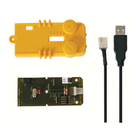
Wiener VM-USB User manual

WIENER, Plein & Baus GmbH 1 www.wiener-d.com
VM-USB
User Manual
Rev. 3.4.1, December 28, 2007

WIENER, Plein & Baus GmbH 2 www.wiener-d.com
General Remarks
The only purpose of this manual is a description of the product. It must not be interpreted a
declaration of conformity for this product including the product and software.
W-Ie-Ne-R revises this product and manual without notice. Differences of the description
in manual and product are possible.
W-Ie-Ne-R excludes completely any liability for loss of profits, loss of business, loss of
use or data, interrupt of business, or for indirect, special incidental, or consequential
damages of any kind, even if W-Ie-Ne-R has been advises of the possibility of such
damages arising from any defect or error in this manual or product.
Any use of the product which may influence health of human beings requires the express
written permission of W-Ie-Ne-R.
Products mentioned in this manual are mentioned for identification purposes only. Product
names appearing in this manual may or may not be registered trademarks or copyrights of
their respective companies.
No part of this product, including the product and the software may be reproduced,
transmitted, transcribed, stored in a retrieval system, or translated into any language in any
form by any means with the express written permission of W-Ie-Ne-R.
VM-USB and CC-USB are designed by JTEC Instruments.

WIENER, Plein & Baus GmbH 3 www.wiener-d.com
Table of contents:
1General Description.........................................................................................................5
1.1 VM-USB Features .................................................................................................. 5
1.2 Data Transfer Modes ........................................................................................... 6
1.3 VM-USB Front panel ........................................................................................... 6
1.4 Technical Data ...................................................................................................... 7
1.5 Power Consumption ............................................................................................. 7
1.6 Block diagram....................................................................................................... 8
2VM-USB and USB driver installation ...........................................................................9
2.1 Installation for Windows Operating Systems .................................................... 9
2.2 Installation for Linux Operating Systems........................................................ 12
2.3 Firmware upgrades ............................................................................................ 12
3General Architecture of VM-USB and its User Interface .........................................14
3.1 Action Register (Address = 1 / 0x1)................................................................... 14
3.2 VME Command Generator / EASY-VME (Address = 4 / 0x4) .................... 15
3.3 VME Command Stacks...................................................................................... 15
3.4 Internal Register File ......................................................................................... 16
3.4.1 Firmware ID Register - Read only .............................................................. 16
3.4.2 Global Mode Register – Read/Write ............................................................ 16
3.4.3 Data Acquisition Settings Register – Read/Write ........................................ 18
3.4.4 User LED Source Selectors – Read /Write.................................................. 18
3.4.5 User Devices Source Selector - Read/Write................................................ 19
3.4.6 Delay and Gate Generator / Pulser Registers – Read/Write......................... 20
3.4.7 Scaler Registers SLR_A and SCLR_B – Read ............................................ 21
3.4.8 Number Extract Mask Register - Read/Write ............................................. 21
3.4.9 Interrupt Service Vectors - Read/Write....................................................... 21
3.4.10 USB Bulk Transfer Setup Register – Read/Write ........................................ 22
3.5 IRQ Mask ............................................................................................................ 22
4COMMUNICATING WITH VM-USB .......................................................................24
4.1 General structure of Out Packets ..................................................................... 24
4.2 Writing Data to the Register Block................................................................... 25
4.3 Reading Back Data from the Register Block ................................................... 25
4.4 Writing Data to the VME Command Stacks / VME Command Generator . 25
4.5 Structure of the VME Stack .............................................................................. 26
4.5.11 Single Transfer Commands .......................................................................... 28
4.5.12 Block Transfer Commands........................................................................... 29
4.5.13 Multiblock Transfer...................................................................................... 29
4.5.14 Writing Marker Words into the Output Data Stream ................................... 29
4.5.15 Use of Hit Registers for Conditional Execution of Stack Commands ......... 30
4.5.16 Using Dynamical Block Sizing for Block Transfers.................................... 30
4.5.17 Using XXUSBWin Application to Handle Stacks ....................................... 31
4.6 Structure of the IN Packets ............................................................................... 32

WIENER, Plein & Baus GmbH 4 www.wiener-d.com
5Guide to List Mode Data Acquisition with VM-USB.................................................35
6LIBXXUSB Library for Windows and Linux ............................................................36
6.1 xxusb_devices_find ............................................................................................. 36
6.2 xxusb_device_open ............................................................................................. 36
6.3 xxusb_serial_open............................................................................................... 37
6.4 xxusb_device_close ............................................................................................. 37
6.5 xxusb_reset_toggle.............................................................................................. 38
6.6 xxusb_register_write .......................................................................................... 38
6.7 xxusb_register_read ........................................................................................... 39
6.8 xxusb_stack_write .............................................................................................. 39
6.9 xxusb_stack_read ............................................................................................... 40
6.10 xxusb_stack_execute........................................................................................... 41
6.11 xxusb_ longstack_execute .................................................................................. 42
6.12 xxusb_usbfifo_read............................................................................................. 43
6.13 xxusb_bulk_read................................................................................................. 43
6.14 xxusb_bulk_write ............................................................................................... 44
6.15 xxusb_flashblock_program ............................................................................... 45
7VM_USB Specific Functions ........................................................................................46
7.1 VME_register_write........................................................................................... 46
7.2 VME_register_read............................................................................................ 46
7.3 VME_DGG.......................................................................................................... 47
7.4 VME_LED_settings............................................................................................ 48
7.5 VME_Output_settings ....................................................................................... 49
7.6 VME_write_32.................................................................................................... 50
7.7 VME_read_32 ..................................................................................................... 51
7.8 VME_write_16.................................................................................................... 51
7.9 VME_read_16 ..................................................................................................... 52
7.10 VME_BLT_read_32 ........................................................................................... 52
8APPENDIX B: Use of Multiplexed User Devices .......................................................56
8.1 Characteristics and the Use of Delay and Gate Generators ........................... 56
8.2 Characteristics and the Use of Scalers.............................................................. 56
9appendix c: enhancments implemented in firmware 95000405 ................................56
10 APPENDIX D: ENHANCMENTS IMPLEMENTED IN FIRMWARE 16000503 57

WIENER, Plein & Baus GmbH 5 www.wiener-d.com
1GENERAL DESCRIPTION
The VM-USB is an intelligent VME master with high speed USB2 interface. Enhanced
functionality is given by the programmable internal FPGA logic which provides a VME
command sequencer with 4kB stack, 4kB event buffer, and 26kB data buffer. Combined
with the 4 front panel I/O ports, this allows VME operation and data acquisition / buffering
without any PC or USB activity, other than reading out suitably formatted data buffers.
The VM-USB can be also programmed to act as a VME slave with respect to a master crate
controller, while performing master operations on other data acquisition modules. For
example, it can be programmed via the VME bus to perform the readout of multiple VME
modules, with data buffering in a 24-kByte FIFO. The master module can then retrieve the
data from the VM-USB alone, at block transfer rates.
All VM-USB logic is controlled by a XC3S400 XILINX Spartan 3 family FPGA. Upon
power-up the FPGA boots from a selected segment (one of four) of flash memory. The
configuration flash memory can be reprogrammed via the USB port, allowing convenient
updates of the firmware. Following an open platform approach, the user can develop his own
FPGA configuration / firmware. The boot sector is selected by setting of a front-panel rotary
switch.
1.1 VM-USB Features
•Low-cost 6U single wide VME master with high speed USB2 interface, auto-
selecting USB2 / USB1, LED’s for speed and FPGA failure/reset..
•While operated as a slot-one system controller, performs round-robin and fair bus
arbitration, generates the 16 MHz system clock, and generates BERR response, when
no DTACK appears within 16us from the assertion of data strobes by any controller.
•May be programmed to service any or all of the 7 interrupt requests IRQ1-7.
•Can generate any of the 7 interrupts when configured with a suitable firmware
•2 multiplexed NIM inputs (with LEMO connectors), with a selection of input signal
functionality including 2 32-bit scalers and 2 delay and gate generators.
•2 multiplexed NIM outputs (with LEMO connectors), with a selection of source
signals, including the outputs of the 2 delay and gate generators.
•4 multiplexed LED’s, with a large selection of diagnostic signals.
•Spartan 3 FPGA, XC3S400 based, firmware upgradeable via the USB port from a
host PC.
•Built in VME sequencer, 1k x 16 bit VME command stack memory for use in an
autonomous data acquisition process. Programmable via USB and/or VME,
depending on the active FPGA firmware.
•Open architecture, allowing the user to develop his own FPGA configuration.
•Readout triggered either via USB link, by VME interrupt (IRQ1-7) or by a start signal
applied to a (programmable) NIM input.
•26-kByte of pipelined data buffer (FIFO) with programmable level of transfer trigger
•Low power consumption, only +5V used.

WIENER, Plein & Baus GmbH 6 www.wiener-d.com
1.2 Data Transfer Modes
•Single word transfer D8, D16, D24, D32 with the full selection of bus placement,
including unaligned transfers.
•Addressing modes A16, A24, A32.
•BLT16, and BLT32 block transfers..
•Multi-BLT transfers of up to 8 Mbytes, both write and read, with or without auto-
increment of individual BLT addresses.
•Autonomous (intelligent) operation pursuant to user-programmed stack. May include
conditional execution of VME commands controlled by the content of a hit register.
May include multiple, conditional command stacks, action triggered by either USB,
VME IRQ, or external signal.
•Highly effective triply-pipelined stack execution, virtually with no band-width
penalty for single (as opposed to block transfer) operations.
•Long USB2 bulk transfers of up to 4 MByte, both write and read.
•Highly customizable.
1.3 VM-USB Front panel
4 user LED’s
Failure LED / USB 1 or 2 indicato
r
2 user outputs Lemo / NIM
USB port
2 user inputs Lemo / NIM
Firmware selector (1 – 4) :
P1 – P4 for programming
C1 – C4 for use / operation

WIENER, Plein & Baus GmbH 7 www.wiener-d.com
1.4 Technical Data
Packaging single wide 6U VME module
Interface USB2 / USB1 auto-detecting / ranging, Connector: USB type B
Inputs 2 user inputs, NIM level , LEMO
Multiplexed functionality (firmware 8504):
Outputs 2 multiplexed outputs for VME, USB and DAQ signals, NIM
level, LEMO, function firmware dependent
Display 4 programmable User LED’s (green, red, green, yellow)
3 USB status LED’s (USB1, USB2, Failure)
VME master modes A16, A24, A32, D8, D16, D24, D32, BLT32, BLT16
System Controller bus arbiter and / or interrupt handler
Firmware Software upgradeable, 4 firmware locations
Selection via 8 position switch (P=program, C=use)
Performance D32 via USB (EASY-VME): 128 kB/s
D32 with data buffering: 32 MB/s
BLT: 32 MB/s
1.5 Power Consumption
Voltage Max. current Power
+5 V 1.2 A about 8 W
1.6 Slave Module Base Address Jumper Settings
The VM-USB module can be used as a VME slave in A32, A24 or A16 mode. For this
purpose the base address BADR can be selected via 5 jumpers, which define bits 27-
31(A32), 20-24(A24) or 12-16 (A16) (always 5 most significant bits of the VME address).
By default the SLAVE Base Address is:
BADR = 0x08 0000 (A24).
BADR = 0x0800 0000 (A32).

WIENER, Plein & Baus GmbH 8 www.wiener-d.com
1.7 Block diagram
I1 - User NIM input
O1 - User NIM "Busy" output
ACQ - Data Acquisition Control
REG - Register Block
STACKS - VME Command Stacks (2 kBytes)
VME command Gen. - VME command Generator
VME - VME Bus, Including Arbitration
FIFOs - Three-Stage Pipelined FIFO array(22 kBytes)
Master - Control Unit
USB Controller - FX2 CY7C68013 IC
OUT FIFO - USB Out FIFO (Relative to Host)
IN FIFO - USB In FIFO (Relative to Host)
VMEBus
FIFOs
OUT FIFO IN FIFO
VME Commnd
Generator
USB CONTROLLER
REG STACKSACQ
I1
MASTER
External to
FPGA
FPG
A
Data
Control
O1
Register
File
User
Devices

WIENER, Plein & Baus GmbH 9 www.wiener-d.com
2VM-USB AND USB DRIVER INSTALLATION
ATTENTION!!! Observe precautions for handling:
•Electrostatic device! Handle only at static safe work stations. Do not touch electronic
components or wiring
•The VME crate as well as the used PC have to be on the same electric potential. Different
potentials can result in unexpected currents between the VM-USB and connected computer which
can destroy the units.
•Do not plug the VC-USB into a VME crate under power. Switch off the VME crate first before
inserting or removing any VME module! For safety reasons the crate should be disconnected
from AC mains.
2.1 Installation for Windows Operating Systems
1. Switch off the VME crate and remove the power cord. Plug in the VM-USB on the first left
slot 1 if needed as system controller and secure it with the front panel screw. Switch on the
VME crate.
2. Insert the driver and software CD-ROM into the CD-ROM drive of the computer and run
the setup program in the XXUSBWin_Install folder. Define directory for installation and
click the installation button.
3. Connect the VM-USB via the provided USB cable to a USB port of the computer. Running
Windows 2000 or XP the hardware change should be detected and the “New Hardware
Wizard” Window should open and show the VME USB controller.
4. Do not use the automatic software installation but chose “installation from specific
location”.

WIENER, Plein & Baus GmbH 10 www.wiener-d.com
5. Select manual search for the driver
6. Type in the drive letter for the CD-ROM (e.g. D:, F:, …) and locate the file CC-USB.inf.
Press Enter to select this driver and to close the window.
7. The WIENER VM-USB driver should be listed and highlighted in the driver list. The driver
is not digitally signed which however does not have any effect on it’s functionality. Press
Next to finish the installation.

WIENER, Plein & Baus GmbH 11 www.wiener-d.com
8. The “New Hardware Wizard” should copy all driver files into the Windows System32
folders and report a successful installation.

WIENER, Plein & Baus GmbH 12 www.wiener-d.com
9. In order to use the XXUSBWin.exe program please install it by running the setup.exe
program in the XXUSBWin---_Install directory (--- select the right Windows version for
your computer).
2.2 Installation for Linux Operating Systems
Linux support for the VM_USB is provided through a shared library and header file. To use
these file simply copy them to an appropriate location, such as /usr/lib for the library and
/usr/include for the header file. All files are open source.
The functions available in the library are exactly the same as those available at for Windows and are described
later in the manual. Linux specific details are located in the readme file on the software CD that you received
with your module.
2.3 Firmware upgrades
The VM-USB is shipped with the latest firmware for the FPGA loaded however, new
versions of it may be available on the web. Please occasionally check at www.wiener-d.com
-> support -> downloads if newer versions of firmware, documentation and / or software are
available.
The firmware upgrade is done via USB and can be performed by the help of the XXUSBWin
program.
To upgrade, switch the firmware selector to one of the 4 firmware programming positions
(P1-P4). The red Failure LED will be on. Start the XXUSBWin program which will show the
following error message:

WIENER, Plein & Baus GmbH 13 www.wiener-d.com
Select “Yes” or go to the Flash ROM Operations page and click program. Open the file of the
latest firmware (xxx.bit)
When done one has to reset the controller or switch the selector switch to the corresponding
run location (C1-C4) and power cycle the crate.

WIENER, Plein & Baus GmbH 14 www.wiener-d.com
3GENERAL ARCHITECTURE OF VM-USB AND ITS USER INTERFACE
Note: The information is this section is relevant only for VM_USB controllers with firmware
950000405 or later. If you have an earlier version consider updating or see Appendix C.
Most of the VM_USB registers take the form of a VME address within the VM_USB and
can be communicated with by using VME calls to the appropriate VME address. These
registers are part of the Internal register file. The registers that cannot be communicated with
in this way are in Table 1.
Table 1. Internal VM)USB registers that aren’t seen as VME space
PA Device
1 Action Register (AR)
4 VME Command Generator (VCG)
- VME Commmand Stacks
- Common Output Buffer
3.1 Action Register (Address = 1 / 0x1)
12-15 8-11 5-7 4 3 2 1 0
- - - scaler dump SYSRES clear USB trigger Start/stop
The action register is a special-purpose write-only register controlling the mode of operation
of VM-USB and the generation of internal trigger/reset signals. By its design, it can often be
accessed when other VM-USB actions are under way and, most notably, when VM-USB is
placed in autonomous data acquisition mode.
Bit 0 of the Action Register controls the operating mode of VM-USB and distinguishes
between the interactive and autonomous data acquisition modes. In the interactive mode,
VME commands (individual or a sequence) are performed directly in response to a USB
packet received from the host, while in the data acquisition mode, sequences of VME
commands are executed, pursuant to lists stored in a dedicated VM-USB memory block. Any
of the configurable 8 lists (stacks) is executed upon the receipt of the associated trigger
signal, which may be a signal at the user NIM input I1, detection of a valid VME IRQ, or a
USB trigger of scaler readout. When bit 0 of the Action Register is set, VM-USB is in data
acquisition mode; otherwise it is in interactive mode.
Bit 1 of the Action Register is a write-only bit, such that writing “1” to it generates an
internal signal of 150ns duration, called USB Trigger. This signal can be routed to user NIM
outputs O1 or O2, used as an input to multiplexed internal user devices of VM-USB (such as
delay and gate generators and scalers), and/or displayed on user LEDs.
Bit 2 of the Action Register is a write-only bit, such that writing “1” to it, clears a number of
internal registers. It is intended primarily for use during firmware debugging.

WIENER, Plein & Baus GmbH 15 www.wiener-d.com
Bit 3 of the Action Register is a write-only bit linked to the SYSRES line, active when VM-
USB is a slot one controller. When set to “1” VM-USB generates SYSRES. When set to “0”,
the SYSRES is cancelled.
Bit 4 (write-only) of the action register is used to trigger scaler readout when VM-USB is in
data acquisition mode. This interactive mode of the scaler readout combines with the two
automatic readout modes (event-based and timer-based) on “whichever-comes-first” basis.
3.2 VME Command Generator / EASY-VME (Address = 4 / 0x4)
The VME Command Generator decodes lists of coded VME commands, submits the
commands for execution in VME cycles, and causes the received data, if any, to be stored in
a 4kB event memory (FIFO). At the end of the list (end of an event), the content of the event
FIFO is compiled into the main data buffer (up to 26 kB), for a subsequent transfer to the
USB controller. The VME Command Generator receives coded data either directly from the
host (in interactive or Easy-VME mode), or reads it from the VME Command Stacks (in
autonomous data acquisition mode). The structure of the list is identical in both modes of
operation and is discussed in detail further below. An integral part of the VME command is
the VME address of a target register/memory location. In the context of the discussed VM-
USB architecture, this VME address is a secondary address and its space includes the internal
VME address space of VM-USB, associated with the internal register file of VM-USB.
3.3 VME Command Stacks
VME Command Stacks (VCS) are used to store suitably formatted lists or sequences of VME
Commands to be performed in response to event trigger signals while VM-USB is operating
in autonomous data acquisition mode of operation (DAQ mode). In this mode of operation,
VM-USB issues VME commands, reads the data received in response to them, and buffers
the data in a data buffer. When the buffer (up to 26kB) is full, VM-USB dumps it to the FIFO
of the USB controller IC for the retrieval by the host. It is this data buffering that allows one
to take advantage of the superior band width of the USB2 interface in bulk transfer mode and
to achieve throughputs in excess of 30 Mbytes/s.
Starting with firmware 16000503 the number of stacks that could be defined was increased
from 2 to 8. The new firmware allows one to define up to 8 stacks, with Stack ID=0-7,
within the allocated memory of 2kBytes = 1kWords. The starting addresses of stacks can be
set arbitrarily. While stacks with ID=2-7 are dedicated to interrupt handling, stacks with
ID=0 and 1 are of dual use. Unless the latter stacks are used for interrupt handling, they
default to a regular stack with ID=0, executed upon trigger pulse (NIM I1 or USBStart) and
the periodic stack with ID=1 (scaler stack).
When not working in DAQ mode, the VME command stacks can also be executed by the
VME Command Generator (VCG). Chapter 4.4 provides details about the VCS and VCG
stack structure and how to write the stack to the VM-USB. Stack instructions and examples
are shown in chapter 4.5.
While any arbitrary block of data can be stored in the stack memory and then read back, all
stacks are expected to contain properly encoded sequences of VME operations and their
associated options, such that they can be meaningfully decoded by the VME Command
Generator module and submitted for execution, while VM-USB operates in autonomous data
acquisition mode.

WIENER, Plein & Baus GmbH 16 www.wiener-d.com
3.4 Internal Register File
Writing/reading to/from the internal register file is done by executing a 32 bit VME
write/read command with the VME offset assigned to a given register, while bit 12 (value
4096) of the VME command word is set to 1. Details about the VME command word are
found in section 4.5
Table 2. Register VME address offsets and their functionality
Offset Register Note
HEX Dec
0x0 0 Firmware ID 32 bits, Read-only
0x4 4 Global Mode 16 bits, Read/Write
0x8 8 Data Acquisition Settings 32 bits, Read/Write
0xC 12 User LED Source Selector 32 bits, Read/Write
0x10 16 User Devices Source Selector 32 bits, Read/Write
0x14 20 DGG_A Delay/Gate Settings 32 bits, Read/Write
0x18 24 DGG_B Delay/Gate Settings 32 bits, Read/Write
0x1C 28 Scaler_A Data 32 bits, Read/Clear/Enable
0x20 32 Scaler_B Data 32 bits, Read/Clear/Enable
0x24 36 Number Extract Mask 32 bits, Read/Write
0x28 40 Interrupt Service Vectors 1 + 2 32 bits, Read/Write
0x2C 44 Interrupt Service Vectors 3 + 4 32 bits, Read/Write
0x30 48 Interrupt Service Vectors 5 + 6 32 bits, Read/Write
0x34 52 Interrupt Service Vectors 7 + 8 32 bits, Read/Write
0x38 56 Extended DGG_A/B Delay Settings 32 bits, Read/Write
0x3C 60 USB Bulk Transfer Setup 32 bits, Read/Write
3.4.1 Firmware ID Register - Read only
Offset = 0 / 0x0
29-31 24-28 16-23 8-15 0-7
Month Year Beta Version Major Revision Minor Revision
This Firmware ID register identifies the acting FPGA firmware in eight hexadecimal digits
MYBBFFRR, where M and Y represent the month and year of creation, B represents beta
version, and F and R represent the firmware main and revision numbers, respectively. Please
see the notes about the different firmware features in the Appendix section of this manual.
3.4.2 Global Mode Register – Read/Write
Offset = 4 / 0x4
The global mode register has the following 16-bit structure:
Bits 15 14 13 12 11 - 9 8 7 6 5 4 3 - 0
Value - BusReq - HeaderOpt - EvtSepOpt - B u f f O p t

WIENER, Plein & Baus GmbH 17 www.wiener-d.com
Firmware 95000405 and later, offers additionally an option to buffer regular data and scaler
data in common data buffers. This option is selected by setting bit 5 of Global Mode Register
to “1” and it allows one to avoid short buffers, which tend to waste the USB bandwidth. In
mixed buffers, scaler events are identified by bit 15 set in the event header word. The global
mode register for firmware 95000405 and later has the following 16-bit structure.
Bits 15 12-14 9-11 8 7 6 5 4 3 - 1
Value - BusReq - HeaderOpt Align32 EvtSepOpt MixtBuff B u f f O p t
The BuffOpt bits (0-3) define the output buffer length. Bit 4 controls the mode of buffer
filling, such that 0 closes buffers at event boundaries and 1 allows spreading events across
the adjacent buffers:
BuffOpt Value Buffer Length (words)
0 13k (default)
1 8k
2 4k
3 2k
4 1k = 1024
5 512
6 256
7 128
8 64
9 Single Event
The MixtBuff=1 selects mixed buffer option which allows one to pack data associated with
different triggers (NIM, scaler, IRQs) into the same data buffers. In mixed buffers, events
associated with different triggers are identified by an Event Type ID encoded in bits 13-15 of
the event header word. Note that the bits 0 to 11 of this word list the event length and bit 12
indicates event length exceeding the length of the 2k Word event assembly buffer (i.e., that
the event is to be continued in next event buffer).
The EvtSepOpt sets the number of event terminator words (hexadecimal 5555 and AAAA),
such that EvtSepOpt=0/1 cause one/two terminator word/s written at the end of each event.
The Align32 bit controls the alignment of data in the data buffer. The default alignment
(Align32=0) is on 16-bit boundaries. Setting Align32=1 causes all header (buffer and event)
and terminator words to be converted to 32-bit words, by adding blank 16-bit words. Also
16-bit data words that may be returned by some VME read commands are converted to 32-bit
numbers.
The HeaderOpt bit controls the structure of the buffer header, such that HeaderOpt=0 writes
out one header word identifying the buffer type (bit 15=1 – watchdog buffer, bit 14=0 – data
buffer, bit 14=1 – scaler buffer) and the number of events in buffer. When HeaderOpt = 1,
the second header word is written out listing the number of words in the buffer.
The BusReq bits identify the VME Bus Request level (0 to 4) to be used by VM-USB, when
not operated as a slot 1 controller (bus arbiter). BusReq=1,2,3, and 4 cause BR0, BR1, BR2,
and BR3 lines to be used, respectively.

WIENER, Plein & Baus GmbH 18 www.wiener-d.com
3.4.3 Data Acquisition Settings Register – Read/Write
Offset = 8 / 0x8
The Data Acquisition Settings register stores the desired readout trigger delay and the scaler
readout mode and frequency. The readout trigger delay represents time in microseconds that
is allowed to lapse, counting from the start signal applied to the NIM I1 input or IRQ
received, before the stack execution is started, and is stored in bits 0-7 of the register. The
scaler readout frequency defines the frequency at which scaler stack is to be executed during
the data acquisition. The stored value is equal to the number of data events separating the
scaler readout events. When the value is zero, scaler readout is suppressed. The number is
stored in bits 16-31 of the register.. The event-based and timer-based triggers are set to
cooperate on “whichever-comes-first” policy.
The composition of the Data Acquisition Settings Register is as follows shown in the table
below
16-31 8-15 0-7
Scaler Readout Frequency Scaler Readout Period Readout Trigger Delay
3.4.4 User LED Source Selectors – Read /Write
Offset = 0x10 / 0xC
The Data stored in this register identifies the sources of the four user LED’s. The actual
selection of sources is firmware specific and subject to customization. The general bit
composition of the selector word is shown in the table below
The 3-bit code identifies the (one-of-eight) source of the signal. The four first sources may
differ for different LED’s, but the last four are shared among all four LED’s. The source
Codes are as follows:
Code Top Yellow Red Green Bottom Yellow
0 USB OutFIFO Not
Empty
Event Trigg. Acquire Not Slot One
1 USB InFIFO Not
Empty
NIM I1 Stack Not Empty USB Trigger
2 Scaler Event NIM I2 Event Ready USB Reset
3 USB InFIFO Full Busy Event Trigger VME BERR
4 VME DTACK VME DTACK VME DTACK VME DTACK
5 VME BERR VME BERR VME BERR VME BERR
6 VME Bus Request VME Bus Request VME Bus Request VME Bus Request
7 VME Bus Granted VME Bus Granted VME Bus Granted VME Bus Granted
LED Unused Bits Latch Bit Invert Bit Code Bits
Top Yellow 5-7 4 3 0-2
Red 13-15 12 11 8-10
Green 21-23 20 19 16-18
Bottom Yellow 29-32 28 27 24-26

WIENER, Plein & Baus GmbH 19 www.wiener-d.com
3.4.5 User Devices Source Selector - Read/Write
Offset = 16 0x10
There are six user devices set up within the FPGA resources of the VM-USB – two NIM
outputs, O1 and O2, two delay and gate generators or pulsers, DGG_1/P_1 and DGG_B/P_1,
and two 32-bit scalers, SCLR_A and SCLR_B. All of these devices may use various signals
as input/trigger signals, with the selection identified by respective code bits stored in the User
Devices Source Selector register. Additionally, this register accommodates bits that enable
and clear the two scalers. The bit composition of the User Devices source selector register is
shown in the table below.
Device Reset Enable Latch Bit Invert Bit Code
NIM O1 - - 4 3 0-2
NIM O2 - - 12 11 8-10
SCLR_A 19 18 - - 16-17
SCLR_B 23 22 - - 20-21
DGG_A - - - 24-26
DGG_B - - - - 28-30
For the NIM outputs a 3-bit code identifies the (1 of 8) source of the signal. Like for LEDs,
the first four sources may differ for different NIM outputs, but the last four are shared., The
source codes are as follows
Code NIM O1 NIM O2
0 Busy USB Trigger
1 Event Trigger Executing VME Command
2 Bus Request VME Address Strobe AS
3 Xfer Event to Data Buffer Xfer Data Buffer to USB FIFO
4 DGG_A DGG_A
5 DGG_B DGG_B
6 End of Event End of Event
7 USB Trigger USB Trigger
Note 1. “Busy” signal indicates that stack processing is in progress, with VME operations not
being completed. “Busy” is asserted when event readout is triggered and removed as soon as
VME operations are completed.
Note 2. “Acquire” indicates that the data acquisition mode is active.
Note 3. “USB Trigger” is generated in response to writing to bit 1 of Action Register.
Note 4. “Event Trigger” indicates that event readout has been triggered.
Note 5. Invert bit causes the signal to be inverted
Note 6. Latch bit causes the signal to be latched. To release the latch one must toggle the bit.
The meaning of the input selector codes for scalers and delay and gate generators is shown in
the table below

WIENER, Plein & Baus GmbH 20 www.wiener-d.com
Code SCLR_A SCLR_B DGG_A/P_A DGG_B/P_B
0 Disabled Disabled Disabled Disabled
1 NIM I1 NIM I1 NIM I1 NIM I1
2 NIM I2 NIM I2 NIM I2 NIM I2
3 Event Event Event Trigger Event Trigger
4 - - End of Event End of Event
5 - - USB Trigger USB Trigger
6 Pulser Pulser
3.4.6 Delay and Gate Generator / Pulser Registers – Read/Write
DGG _A Offset = 20 / 0x14
DGG _B Offset = 24 / 0x18
DGG _ Ext Offset =56/0x38
The two Delay and Gate Generator / Pulser Registers DGG_A and DGG_B as well as the
DGG_ Extend register store data defining the length of the delay and the length of the gate in
units of 12.5 ns (80 MHz clock) for either the gate and delay generator or for the pulser.
These values can be set for channel A and B independently. The pulser is re-triggering after
the defined delay time, i.e. the delay time + gate length defines the pulser repetition rate. The
value of the delay is a composite of a high resolution value (12.5ns) and a coarse range value
which was added with firmware 6.0 to increase the possible time range up to 53.5s . Earlier
firmware versions use only the fine (12.5ns) value.
DGG_A 16-31 DGG_A 0-15
Gate Delay_fine
DGG_B Offset = 24 / 0x18
DGG_B 16-31 DGG_ B 0-15
Gate Delay_fine
DGG_ Ext Offset =56/0x38
DGG_B Ext (16-31) DGG_A Ext 0-15
Delay coarse Delay coarse
Gate len
g
th = 12.5ns * Gate
Delay = 12.5ns * Delay_fine + 819.2
µ
s* Delay_coarse
Pulser repetition period= Gate + Delay
Table of contents


