Wolfson WM9090 User manual

w WM9090
Ultra Low Power Audio Subsystem
WOLFSON MICROELECTRONICS plc
[1] This product is protected by US Patents 7,622,984 and 7,626,445
To receive regular email updates, sign up at http://www.wolfsonmicro.com/enews
Production Data, November 2010, Rev 4.1
Copyright ©2010 Wolfson Microelectronics plc
DESCRIPTION
The WM9090[1] is a high performance low power audio
subsystem with integrated headphone driver and Class D
speaker driver. The speaker driver supports 750mW output
power at 3.7V, 1%THD.
The unique dual mode charge pump architecture provides
ground referenced headphone outputs, removing the
requirement for external coupling capacitors. Class G
technology is integrated to increase the efficiency and
extend playback time by optimizing the headphone driver
supply voltages according to the volume control.
The flexible input configuration allows single ended or
differential stereo inputs. Mixers allow highly flexible routing
to the outputs.
Separate mixer and volume controls are provided for each
headphone and speaker driver. Automatic Gain Control
limits the speaker output signal in order to prevent clipping.
DC offset correction to less than 1mV guarantees a
pop/click-free headphone start up.
WM9090 is controlled using a two-wire I2C interface. An
integrated oscillator generates all internal clocks, removing
the need to provide any external clock.
WM9090 is available in a 2.53mm x 2.07mm 20-bump CSP
package.
FEATURES
•Mono Class D speaker driver
- 2W at 5V SPKVDD @ 1% THD+N into 4
- 950mW at 4.2V SPKVDD @ 1% THD+N into 8
- 90dB SNR
•Ground referenced stereo headphone driver
- 35mW into 16load @ 1% THD+N
- 95dB SNR
- 80dB THD+N
•Differential and single ended analogue input configurations
•Integrated oscillator for clocking requirements
•I
2C 2-wire software control interface
•Automatic gain control (AGC) for speaker output
•SilentSwitch™ Pop and click suppression
- < 1mV DC offset
•<50ms start up time
•Excellent RF and TDMA noise immunity
•Ultra low power consumption
- 4mW quiescent for headphone driver
- 5mW quiescent for speaker driver
•Shutdown current < 1uA
•Supply voltage
- SPKVDD = 2.7V to 5.5V
- AVDD = 1.8V
•1.8V to 2.7V control interface compatibility
•20-bump CSP package
APPLICATIONS
•Mobile handsets
BLOCK DIAGRAM
SPKVDD
SPKOUTP
SPKOUTN
VMIDCSCLK GND
HPOUTL
HPOUTR
Automatic Gain
Control
Control Interface
CPVOUTN
CPVOUTP
CPCA
CPCB
Charge
Pump
+6dB to -57dB
in 1dB steps
+6dB to -57dB
in 1dB steps
IN1N
SDA
IN1P
+6dB to -57dB in
1dB steps
Speaker
VMID
VMID
AVDD
-6dB to 18dB
-6dB to 18dB
Boost Amplifier
Class D Driver
WM9090
DC Offset Correction
+
0dB, -6dB,
-9dB, -12dB
0dB, -6dB,
-9dB, -12dB
+
IN2N
IN2P
VMID
VMID
-6dB to 18dB
-6dB to 18dB
0dB, -6dB,
-9dB, -12dB
+

WM9090 Production Data
w PD, November 2010, Rev 4.1
2
TABLE OF CONTENTS
DESCRIPTION .......................................................................................................1
FEATURES.............................................................................................................1
APPLICATIONS .....................................................................................................1
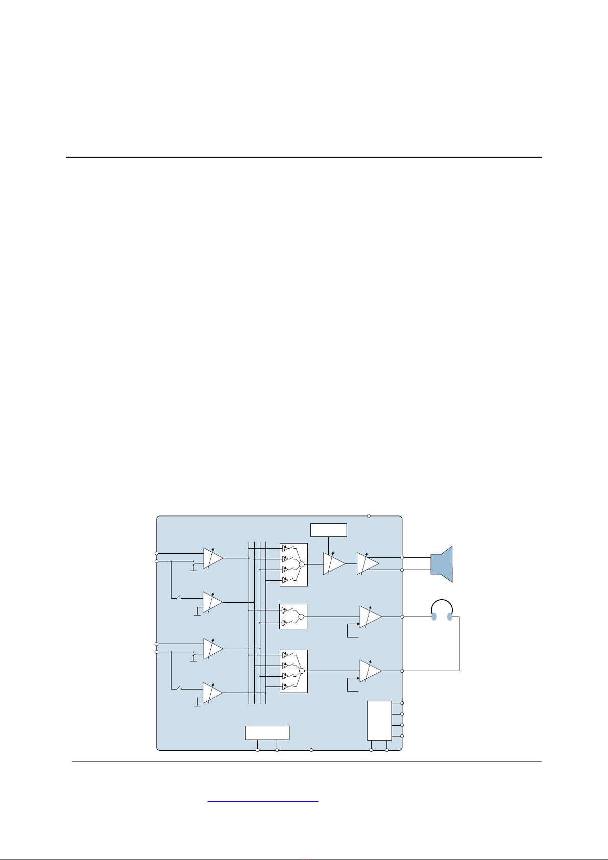
BLOCK DIAGRAM .................................................................................................1
TABLE OF CONTENTS .........................................................................................2
PIN CONFIGURATION...........................................................................................4
ORDERING INFORMATION ..................................................................................4
PIN DESCRIPTION ................................................................................................5
ABSOLUTE MAXIMUM RATINGS.........................................................................6
RECOMMENDED OPERATING CONDITIONS .....................................................6
ELECTRICAL CHARACTERISTICS ......................................................................7
TERMINOLOGY............................................................................................................. 9
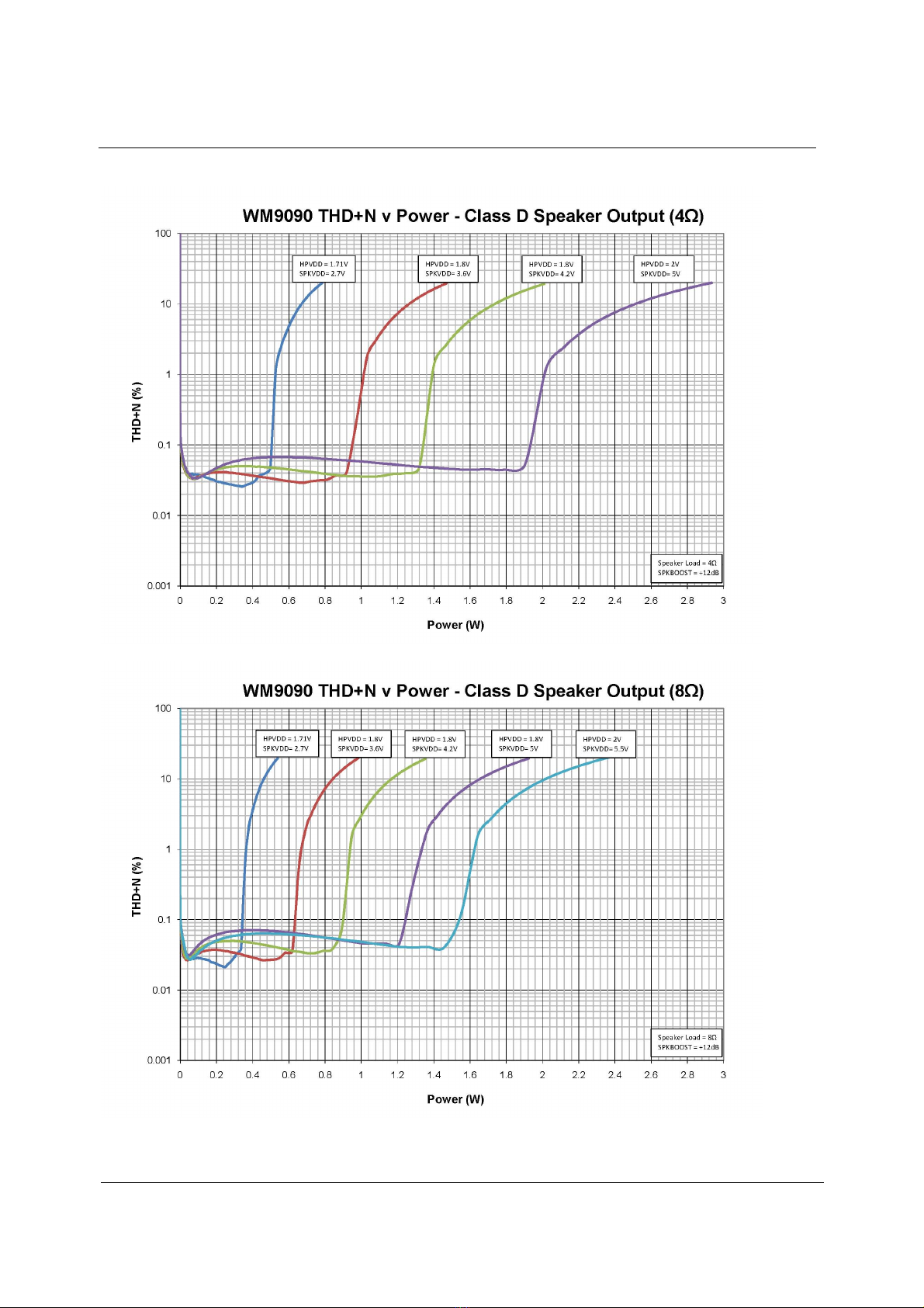
PERFORMANCE PLOTS............................................................................................. 10
TYPICAL PERFORMANCE..................................................................................11
POWER CONSUMPTION............................................................................................ 11
AUDIO SIGNAL PATHS DIAGRAM .....................................................................12
CONTROL INTERFACE TIMING .........................................................................13
DEVICE DESCRIPTION.......................................................................................14
INTRODUCTION.......................................................................................................... 14
INPUT SIGNAL PATH.................................................................................................. 15
LINE INPUTS ............................................................................................................................................ 16
INPUT PGA ENABLE ................................................................................................................................ 16
INPUT PGA CONFIGURATION ................................................................................................................ 17
INPUT PGA VOLUME CONTROL............................................................................................................. 17
OUTPUT SIGNAL PATH.............................................................................................. 20
OUTPUT SIGNAL PATHS ENABLE.......................................................................................................... 20
SPEAKER MIXER CONTROL ................................................................................................................... 21
SPEAKER OUTPUT VOLUME CONTROL................................................................................................ 22
SPEAKER BOOST MIXER CONTROL...................................................................................................... 22
HEADPHONE MIXER CONTROL ............................................................................................................. 23
HEADPHONE OUTPUT VOLUME CONTROL.......................................................................................... 24
AUTOMATIC GAIN CONTROL (AGC) ......................................................................... 27
AGC CONTROL ........................................................................................................................................ 27
AGC ANTI-CLIP ........................................................................................................................................ 27
AGC POWER LIMITING............................................................................................................................ 29
ANALOGUE OUTPUTS ............................................................................................... 31
SPEAKER OUTPUT CONFIGURATIONS................................................................................................. 31
HEADPHONE OUTPUT CONFIGURATIONS ........................................................................................... 32
CLOCKING CONTROL ................................................................................................ 32
CONTROL INTERFACE .............................................................................................. 34
CONTROL WRITE SEQUENCER................................................................................ 37
INITIATING A SEQUENCE ....................................................................................................................... 37
PROGRAMMING A SEQUENCE .............................................................................................................. 38
DEFAULT SEQUENCES........................................................................................................................... 40
POWER SEQUENCES AND POP SUPPRESSION CONTROL .................................. 43
INPUT VMID CLAMPS .............................................................................................................................. 43
HEADPHONE ENABLE/DISABLE............................................................................................................. 43
RECOMMENDED HEADPHONE START UP SEQUENCE....................................................................... 45

Production Data WM9090
wPD, November 2010, Rev 4.1
3
CHARGE PUMP........................................................................................................... 47
DC SERVO .................................................................................................................. 48
DC SERVO ENABLE AND START-UP ..................................................................................................... 48
DC SERVO ACTIVE MODES .................................................................................................................... 50
DC SERVO READBACK ........................................................................................................................... 51
REFERENCE VOLTAGES AND MASTER BIAS.......................................................... 52
POWER MANAGEMENT ............................................................................................. 53
THERMAL SHUTDOWN .............................................................................................. 55
SOFTWARE RESET AND CHIP ID ............................................................................. 55
REGISTER MAP...................................................................................................56
REGISTER BITS BY ADDRESS .................................................................................. 58
APPLICATIONS INFORMATION .........................................................................74
RECOMMENDED EXTERNAL COMPONENTS........................................................... 74
AUDIO INPUT PATHS............................................................................................................................... 75
POWER SUPPLY DECOUPLING ............................................................................................................. 76
HEADPHONE OUTPUT PATH.................................................................................................................. 76
CLASS D SPEAKER CONNECTIONS ...................................................................................................... 77
PCB LAYOUT CONSIDERATIONS.............................................................................. 79
CLASS D LOUDSPEAKER CONNECTION .............................................................................................. 79
PACKAGE DIMENSIONS ....................................................................................80
IMPORTANT NOTICE ..........................................................................................81
ADDRESS:................................................................................................................... 81

WM9090 Production Data
w PD, November 2010, Rev 4.1
4
PIN CONFIGURATION
20-bump CSP package; Top View
ORDERING INFORMATION
ORDER CODE TEMPERATURE RANGE PACKAGE MOISTURE
SENSITIVITY LEVEL
PEAK SOLDERING
TEMPERATURE
WM9090ECS/R -40°C to +85°C 20-ball W-CSP
(Pb-free, Tape and reel) MSL1 260°C
Note:
Reel quantity = 5000

Production Data WM9090
wPD, November 2010, Rev 4.1
5
PIN DESCRIPTION
PIN NO NAME TYPE DESCRIPTION
A1 SPKOUTN Analogue Output Speaker negative output
A2 SPKVDD Supply Speaker supply
A3 DNC n/a Do Not Connect
A4 IN2N Analogue Input
IN2 negative analogue input
A5 IN2P Analogue Input
IN2 positive analogue input
B1 SPKOUTP Analogue Output Speaker positive output
B2 GND Supply Ground for speaker and charge pump
B3 DNC n/a Do Not Connect
B4 IN1N Analogue Input
IN1 negative analogue input
B5 IN1P Analogue Input
IN1 positive analogue input
C1 CPVOUTP Analogue Output
Charge pump positive rail decoupling pin
C2 AVDD Supply Analogue supply
C3 SCLK Digital Input
Control interface clock
C4 SDA Digital Input / Output Control interface data
C5 VMIDC Analogue Output
Mid-rail voltage decoupling pin
D1 CPCB Analogue Output
Charge pump flyback capacitor pin
D2 CPCA Analogue Output
Charge pump flyback capacitor pin
D3 CPVOUTN Analogue Output
Charge pump negative rail decoupling pin
D4 HPOUTL Analogue Output
Left headphone output
D5 HPOUTR Analogue Output
Right headphone output

WM9090 Production Data
w PD, November 2010, Rev 4.1
6
ABSOLUTE MAXIMUM RATINGS
Absolute Maximum Ratings are stress ratings only. Permanent damage to the device may be caused by continuously
operating at or beyond these limits. Device functional operating limits and guaranteed performance specifications are given
under Electrical Characteristics at the test conditions specified.
ESD Sensitive Device. This device is manufactured on a CMOS process. It is therefore generically susceptible
to damage from excessive static voltages. Proper ESD precautions must be taken during handling and storage
of this device.
Wolfson tests its package types according to IPC/JEDEC J-STD-020B for Moisture Sensitivity to determine acceptable storage
conditions prior to surface mount assembly. These levels are:
MSL1 = unlimited floor life at <30°C / 85% Relative Humidity. Not normally stored in moisture barrier bag.
MSL2 = out of bag storage for 1 year at <30°C / 60% Relative Humidity. Supplied in moisture barrier bag.
MSL3 = out of bag storage for 168 hours at <30°C / 60% Relative Humidity. Supplied in moisture barrier bag.
The Moisture Sensitivity Level for each package type is specified in Ordering Information.
CONDITION MIN MAX
Supply voltages (AVDD) -0.3V +2.5V
Supply voltages (SPKVDD) -0.3V +7.0V
Voltage range digital inputs (SCLK, SDA) GND -0.3V +3.3V
Voltage range analogue inputs GND -0.3V +3.3V
Operating temperature range, TA-40ºC +85ºC
Junction temperature, TJMAX -40ºC +150ºC
Storage temperature after soldering -65ºC +150ºC
RECOMMENDED OPERATING CONDITIONS
PARAMETER SYMBOL MIN TYP MAX UNIT
Charge Pump supply range AVDD 1.71 1.8 2.0 V
Speaker supply range SPKVDD 2.7 3.6 5.5 V
Ground GND 0 V

Production Data WM9090
wPD, November 2010, Rev 4.1
7
ELECTRICAL CHARACTERISTICS
Test Conditions
SPKVDD = 3.6V, AVDD=1.8V, GND=0V, TA = +25oC, 1kHz signal, PGA gain = 0dB unless otherwise stated
PARAMETER TEST CONDITIONS MIN TYP MAX UNIT
Analogue Input Pins
Maximum Full-Scale input signal
level - IN1P/N and IN2P/N
Single-ended input 1.0 Vrms
Differential input 1.0
Input Resistance Differential or Single- Ended Mode 8 10 15 kΩ
Input Programmable Gain Amplifiers (PGAs) IN1A, IN1B, IN2A and IN2B
Minimum Programmable Gain -6
dB
Maximum Programmable Gain +18
dB
Mute Attenuation 80
dB
Common Mode Rejection Ratio Differential Mode (217Hz input) 45 dB
Output Programmable Gain Amplifiers (PGAs) SPKVOL, HPOUT1LVOL and HPOUT1RVOL
Minimum Programmable Gain -57
dB
Maximum Programmable Gain +6
dB
Programmable Gain Step Size 1
dB
Mute Attenuation HPOUT1LVOL and HPOUT1RVOL 75 dB
SPKVOL 66
dB
Speaker Output Programmable Gain SPKOUTLBOOST
Programmable Gain SPKOUTLBOOST=111 11.5 12
12.5 dB
SPKOUTLBOOST=110 8.5 9
9.5
SPKOUTLBOOST=101 7 7.5
8
SPKOUTLBOOST=100 5.5 6
6.5
SPKOUTLBOOST=011 4 4.5
5
SPKOUTLBOOST=010 2.5 3
3.5
SPKOUTLBOOST=001 1 1.5
2
SPKOUTLBOOST=000 -0.75 0
0.75
Headphone Driver Audio Performance (RL= 16Ω)
SNR (A-weighted) Path from IN1P/N or IN2P/N 90 96 dB
THD (PO=20mW) -82 dB
THD+N (PO=20mW) -80 -72 dB
THD (PO=5mW) -81 dB
THD+N (PO=5mW) -79 dB
Crosstalk (L/R) 72 dB
PSRR AVDD with 100mVpk-pk at 217Hz (Note 1) 82 dB
SPKVDD with 100mVpk-pk at 217Hz 85
DC Offset Magnitude after DC Servo calibration 0.3 2 mV
Output Power 0.1% THD+N 31
mW
1% THD+N 34
Minimum Headphone Resistance Normal operation 15
Ω
Device survival with load indefinitely applied 1 Ω
Headphone Capacitance
2
nF
Quiescent Current
4
mA

WM9090 Production Data
w PD, November 2010, Rev 4.1
8
Test Conditions
SPKVDD = 3.6V, AVDD=1.8V, GND=0V, TA = +25oC, 1kHz signal, PGA gain = 0dB unless otherwise stated
PARAMETER TEST CONDITIONS MIN TYP MAX UNIT
Speaker Driver Class D Audio Performance (RL=8Ω+ 10μH BTL)
SNR (A-weighted) Speaker Boost = 6dB, 82 92 dB
THD (PO=500mW) Speaker Boost = 6dB -75 dB
THD+N (PO=500mW) Speaker Boost = 6dB -73 dB
PSRR AVDD with 100mVpk-pk at 217Hz (Note 1) 75 dB
SPKVDD with 100mVpk-pk at 217Hz 70 dB
DC Offset at Load 5 mV
Efficiency Speaker Boost = 6dB, 0dBFS input 80 89 %
Output Power SPKVDD=5.0V, THD+N ≤1%,
Speaker Boost = 12dB
1300 mW
SPKVDD=4.2V, THD+N ≤1%,
Speaker Boost = 12dB
950 mW
SPKVDD=3.7V, THD+N ≤1%,
Speaker Boost = 12dB
750 mW
Quiescent Current
3
mA
Leakage Currents
SVDD Leakage Current
0.2 μA
HPVDD Leakage Current VMID_ENA = 0, VMID_BUF_ENA = 0, and
TSHUT_ENA = 0
1
μA
Analogue Reference Level
VMID Midrail Reference Voltage -3%
AVDD/2 +3% V
Charge Pump
Start-up Time 500 μs
Supply Voltage 1.71 2.0 V
CPVOUTP Normal mode AVDD V
Low power mode AVDD/2
CPVOUTN Normal mode -AVDD V
Low power mode -AVDD/2
Flyback Capacitor
(between CPCA and CPCB)
at 2V 1 2.2 μF
CPVOUTP Capacitor at 2V 2 2.2 μF
CPVOUTN Capacitor at 2V 2 2.2 μF
Digital Input / Output
Input HIGH Level 0.7 ×
AVDD
V
Input LOW Level 0.3 ×
AVDD
V
Output HIGH Level IOL = 1mA 0.7 ×
AVDD
V
Output LOW Level IOH = -1mA 0.3 ×
AVDD
V
Input capacitance 10 pF
Input leakage -0.9 0.9 uA
Start-Up Time
Start up time Speaker and Headphone -35 ms
Note 1: Total system PSRR with external DC-DC or LDO will be higher

Production Data WM9090
wPD, November 2010, Rev 4.1
9
TERMINOLOGY
1. Signal-to-Noise Ratio (dB) – SNR is a measure of the difference in level between the maximum full scale output
signal and the output with no input signal applied.
2. Total Harmonic Distortion (dB) – THD is the level of the rms value of the sum of harmonic distortion products relative
to the amplitude of the measured output signal.
3. Total Harmonic Distortion plus Noise (dB) – THD+N is the level of the rms value of the sum of harmonic distortion
products plus noise in the specified bandwidth relative to the amplitude of the measured output signal.
4. Crosstalk (L/R) (dB) – left-to-right and right-to-left channel crosstalk is the measured signal level in the idle channel at
the test signal frequency relative to the signal level at the output of the active channel. The active channel is
configured and supplied with an appropriate input signal to drive a full scale output, with signal measured at the
output of the associated idle channel.
5. Mute Attenuation – This is a measure of the difference in level between the full scale output signal and the output with
mute applied.
6. All performance measurements carried out with 20kHz low pass filter, and where noted an A-weighted filter. Failure to
use such a filter will result in higher THD and lower SNR readings than are found in the Electrical Characteristics. The
low pass filter removes out of band noise; although it is not audible it may affect dynamic specification values.

WM9090 Production Data
w PD, November 2010, Rev 4.1
10
PERFORMANCE PLOTS

Production Data WM9090
wPD, November 2010, Rev 4.1
11
TYPICAL PERFORMANCE
POWER CONSUMPTION
SVDD HPVDD iSVDD iHPVDD Total Power
(V) (V) (μA) (μA) (μW)
All supplies except SVDD disabled 3.6 0.0 0.2 0.0 0.72
All supplies enabled VMID_ENA = 0, VMID_BUF_ENA =
0, 3.6 1.8 0.2 2 4.3
SPKKVDD LDO1VDD iSPKVDD iLDO1VDD Tota l Power
(V) (V) (mA) (mA) (mW)
IN1+/IN1- Stereo to Headphone 16ohm load 3.6 1.8 0.00 3.36 6.0
IN2+/IN2- Differential to Speaker Class D 8ohm + 10μH, +6dB boost 3.6 1.8 2.54 1.56 12.0
Speaker
Shutdown Leakage
Mode Other settings
Battery Leakage
Mode Other settings
Headphone
Notes:
1. Power in the load is included
2. All figures are quoted at TA = 25°C
3. All figures are quoted as quiescent current unless otherwise stated

WM9090 Production Data
w PD, November 2010, Rev 4.1
12
AUDIO SIGNAL PATHS DIAGRAM
HPOUTL
SPKOUTN
SPKOUTP
SPKMIXL
MIXOUTL
MIXOUTR
SPKOUTLBOOST
HPOUT1LVOL
SPKLVOL
HPOUT1L_MUTE
HPOUT1L_VOL[5:0]
SPKOUTL_MUTE
SPKOUTL_VOL[5:0]
SPKMIXL_TO_SPKOUTL
SPKOUTL_BOOST[2:0]
SPKOUTL_ENA
SPKMIX_ENA
MIXOUTL_ENA
HPOUT1L_ENA
IN1A
IN1B
IN1B_ENA
IN1A_MUTE
IN1A_VOL[2:0]
IN1A_ENA
IN1B_MUTE
IN1B_VOL[2:0]
+
IN1A_TO_SPKMIX / IN1A_SPKMIX_VOL
IN1B_TO_SPKMIX / IN1B_SPKMIX_VOL
IN2A_TO_SPKMIX / IN2A_SPKMIX_VOL
IN2B_TO_SPKMIX / IN2B_SPKMIX_VOL
IN1A_TO_MIXOUTL / IN1A_MIXOUTL_VOL
IN2A_TO_MIXOUTL / IN2A_MIXOUTL_VOL
SPKLVOL_ENA
SPKMIX_MUTE
MIXOUTL_MUTE
HPOUTR
DC Offset Correction
HPOUT1RVOL
HPOUT1R_MUTE
HPOUT1R_VOL[5:0] HPOUT1R_ENA
DC Offset Correction
IN1_DIFF
IN1P
IN1N
+
MIXOUTR_ENA
+
IN1A_TO_MIXOUTR / IN1A_MIXOUTR_VOL
IN1B_TO_MIXOUTR / IN1B_MIXOUTR_VOL
IN2A_TO_MIXOUTR / IN2A_MIXOUTR_VOL
IN2B_TO_MIXOUTR / IN2B_MIXOUTR_VOL
MIXOUTR_MUTE
IN2A
IN2B
IN2B_ENA
IN2A_MUTE
IN2A_VOL[2:0]
IN2A_ENA
IN2B_MUTE
IN2B_VOL[2:0]
IN2_DIFF
IN2P
IN2N

Production Data WM9090
wPD, November 2010, Rev 4.1
13
CONTROL INTERFACE TIMING
SCLK
(input)
SDA
t4t3
START
t8
STOP
t5
t2t1
t9
t7
t6
Figure 1 Control Interface Timing
Test Conditions
SPKVDD = 3.6V, AVDD=1.8V, GND=0V, TA = +25oC, 1kHz signal, PGA gain = 0dB unless otherwise stated
PARAMETER SYMBOL MIN TYP MAX UNIT
SCLK Frequency 400 kHz
SCLK Low Pulse-Width t11300 ns
SCLK High Pulse-Width t2600 ns
Hold Time (Start Condition) t3600 ns
Setup Time (Start Condition) t4600 ns
Data Setup Time t5100 ns
SDA, SCLK Rise Time t6300 ns
SDA, SCLK Fall Time t7300 ns
Setup Time (Stop Condition) t8600 ns
Data Hold Time t9900 ns
Pulse width of spikes that will be suppressed tps 0 5 ns

WM9090 Production Data
w PD, November 2010, Rev 4.1
14
DEVICE DESCRIPTION
INTRODUCTION
The WM9090 is an ultra-low power, high quality audio subsystem, including a headphone and
speaker driver. Its flexible architecture is designed to interface with a wide range of analogue
components. The small 2.0 x 2.5mm footprint makes it ideal for portable applications such as mobile
handsets.
Four flexible analogue input pins allow interfacing to up to four single-ended sources (eg. two stereo
signal pairs). A differential input can also be accommodated if required. Connection to an external
voice CODEC, FM radio, melody IC or generic line input are all fully supported. Signal routing to the
output mixers provides maximum flexibility to support a wide variety of usage modes.
Three analogue output drivers are integrated, including a high quality Class D speaker driver
supporting 750mW output power at 3.7V. A configurable automatic gain control (AGC) is provided on
the speaker output path, to prevent clipping or power overload at the loudspeaker.
Ground-referenced stereo headphone outputs are also provided; these are powered from an
integrated Charge Pump, enabling high quality, power efficient headphone playback. The ground-
referenced design reduces power consumption, improves bass response, and enables direct
headphone connection without any DC blocking capacitors. A DC Servo circuit is provided for DC
offset measurement and correction, thereby suppressing pops and reducing power consumption.
Internal differential signal routing and amplifier configurations have been optimised to provide the
lowest possible power consumption for a wide range of usage scenarios, including voice calls and
music playback. The speaker drivers offer low leakage and high PSRR; this enables direct
connection to a Lithium battery. The speaker driver provides eight levels of boost gain to allow output
signal levels to be maximised for many commonly-used SPKVDD/AVDD combinations.
An integrated oscillator is provided to support all the WM9090 clocking requirements, including the
Class D switching clock, Headphone Charge Pump and DC Servo control.
The WM9090 is controlled via a standard 2-wire I2C interface, providing full software control of all
features, together with device register readback. The interface provides support for I/O voltages up to
2.7V. An integrated Control Write Sequencer enables automatic scheduling of control sequences;
commonly-used signal configurations may be selected using ready-programmed sequences,
including time-optimised control of the WM9090 pop suppression features. Unused circuitry can be
disabled under software control, in order to save power; low leakage currents enable extended
standby/off time in portable battery-powered applications.

Production Data WM9090
wPD, November 2010, Rev 4.1
15
INPUT SIGNAL PATH
The WM9090 supports two differential analogue input channels, configurable in a number of
combinations:
•Up to two differential line inputs to analogue mixers
•Up to four single-ended line inputs to analogue mixers
The inputs may be mixed together or independently routed to different combinations of output
drivers. The WM9090 input signal paths and control registers are illustrated in Figure 2.
Figure 2 Control Registers for Input Signal Path

WM9090 Production Data
w PD, November 2010, Rev 4.1
16
LINE INPUTS
All of the analogue input pins are designed as line inputs. These pins can be configured as single-
ended or differential inputs, with flexible routing options and gain controls suitable for many different
usage cases. These inputs provide a high gain path for low input signal levels.
The line input pins IN1P and IN1N provide a differential input path to PGA IN1A. If required, these
input pins can be configured as two separate single-ended inputs to PGAs IN1A and IN1B
respectively. Single ended configuration is selected by writing a 0 to the IN1_DIFF register bit.
The line input pins IN2P and IN2N provide a differential input path to PGA IN2A. If required, these
input pins can be configured as two separate single-ended inputs to PGAs IN2A and IN2B
respectively. Single ended configuration is selected by writing a 0 to the IN2_DIFF register bit.
Signal path configuration to the input PGAs is detailed later in this section. Signal path configuration
to the output mixers and speaker mixers is described in “Output Signal Path”.
Note that, by default, the analogue input pins are clamped to VMID in order to prevent audible pops
caused by enabling the input paths. When one or more analogue input path is in use, the respective
input clamp(s) must be disabled using the register bits described under “Power Sequences and Pop
Suppression Control”.
INPUT PGA ENABLE
The Input PGAs are enabled using register bits IN1A_ENA, IN1B_ENA, IN2A_ENA and IN2B_ENA,
as described in Table 1. The Input PGAs must be enabled for line input on the respective input pins.
Note that, for differential input on IN1P and IN1N, it is not necessary to enable PGA IN1B.
Note that, for differential input on IN2P and IN2N, it is not necessary to enable PGA IN2B.
REGISTER
ADDRESS
BIT LABEL DEFAULT DESCRIPTION
R2 (02h)
Power
Management
(2)
7 IN1A_ENA 0 IN1A Input PGA Enable
0 = Disabled
1 = Enabled
6 IN1B_ENA 0 IN1B Input PGA Enable
0 = Disabled
1 = Enabled
(Note this is only required for single-ended
input on the IN1N pin)
5 IN2A_ENA 0 IN2A Input PGA Enable
0 = Disabled
1 = Enabled
4 IN2B_ENA 0 IN2B Input PGA Enable
0 = Disabled
1 = Enabled
(Note this is only required for single-ended
input on the IN2N pin)
Table 1 Input PGA Enable
For normal operation of the input PGAs, the reference voltage VMID and the bias current must also
be enabled. See “Reference Voltages and Master Bias” for details of the associated controls
VMID_RES and BIAS_ENA.

Production Data WM9090
wPD, November 2010, Rev 4.1
17
INPUT PGA CONFIGURATION
The input PGAs can be configured in single-ended mode or differential mode, using the IN1_DIFF
and IN2_DIFF register bits described in Table 2.
In single-ended mode, an input pin is routed to each individual PGA. In differential mode, a pair of
input pins is routed to PGA IN1A or IN2A.
REGISTER
ADDRESS
BIT LABEL DEFAULT DESCRIPTION
R22 (16h)
IN1 Line
Control
1 IN1_DIFF 1 PGA IN1A and IN1B configuration
0 = Single-ended mode
1 = Differential mode
R23 (17h)
IN2 Line
Control
1 IN2_DIFF 1 PGA IN2A and IN2B configuration
0 = Single-ended mode
1 = Differential mode
Table 2 Input PGA Configuration
INPUT PGA VOLUME CONTROL
Each of the four input PGAs has an independently controlled gain range of -6dB to +18dB. The gains
on the inverting and non-inverting inputs to the PGAs are always equal. Each Input PGA can be
independently muted using the PGA mute bits as described in Table 3.
Note that, when input pins IN1P and IN1N are configured in differential mode, then PGA IN1B is not
used, and the volume control is provided on PGA IN1A only.
Note that, when input pins IN2P and IN2N are configured in differential mode, then PGA IN2B is not
used, and the volume control is provided on PGA IN2A only.
The gain level of PGA IN1A and IN2A differs between single-ended and differential mode. For
example, a 0dB volume setting provides 0dB gain in differential mode, but in single-ended mode it
will apply +6dB gain. In single-ended mode, the IN1A/IN2A input PGAs have a controlled gain range
of 0dB to +24dB. In differential mode, these PGAs have a controlled gain range of -6dB to +18dB.
To prevent "zipper noise", a zero-cross function is provided on the input PGAs. When this feature is
enabled, volume updates will not take place until a zero-crossing is detected. In the case of a long
period without zero-crossings, a timeout function is provided. When the zero-cross function is
enabled, the volume will update after the timeout period if no earlier zero-cross has occurred. The
timeout clock is enabled using TOCLK_ENA, the timeout period is set by TOCLK_RATE. See
“Clocking Control” for more information on these fields.
The IN1_VU and IN2_VU bits control the loading of the input PGA volume data. When IN1_VU and
IN2_VU are set to 0, the PGA volume data will be loaded into the respective control register, but will
not actually change the gain setting. The IN1A and IN1B volume settings are both updated when a 1
is written to IN1_VU; the IN2A and IN2B volume settings are both updated when a 1 is written to
IN2_VU. This makes it possible to update the gain of two single-ended input paths simultaneously.
Note that, in differential input modes, the Volume Update control bits IN1_VU and/or IN2_VU should
always be set to 1.
The Input PGA Volume Control register fields are described in Table 3.
REGISTER
ADDRESS
BIT LABEL DEFAULT DESCRIPTION
R24 (18h)
IN1 Line Input
A Volume
8 IN1_VU N/A IN1 Volume Update
Writing a 1 to this bit will cause IN1A and
IN1B input PGA volumes to be updated
simultaneously
7 IN1A_MUTE 1 IN1A PGA Mute
0 = Un-Mute
1 = Mute
6 IN1A_ZC 0 IN1A PGA Zero Cross Control
0 = Change gain immediately
1 = Change gain on zero cross only

WM9090 Production Data
w PD, November 2010, Rev 4.1
18
REGISTER
ADDRESS
BIT LABEL DEFAULT DESCRIPTION
2:0 IN1A_VOL
[2:0]
011 IN1A Volume (differential mode)
000 = -6dB
001 = -3.5dB
010 = 0dB
011 = +3.5dB
100 = +6dB
101 = +12dB
110 = +18dB
111 = +18dB
IN1A Volume (single-ended mode)
000 = 0dB
001 = +2.5dB
010 = +6dB
011 = +9.5dB
100 = +12dB
101 = +18dB
110 = +24dB
111 = +24dB
R25 (19h)
IN1 Line Input
B Volume
8 IN1_VU N/A IN1 Volume Update
Writing a 1 to this bit will cause IN1A and
IN1B input PGA volumes to be updated
simultaneously
7 IN1B_MUTE 1 IN1B PGA Mute
0 = Un-Mute
1 = Mute
6 IN1B_ZC 0 IN1B PGA Zero Cross Control
0 = Change gain immediately
1 = Change gain on zero cross only
2:0 IN1B_VOL
[2:0]
011 IN1B Volume (differential mode)
000 = -6dB
001 = -3.5dB
010 = 0dB
011 = +3.5dB
100 = +6dB
101 = +12dB
110 = +18dB
111 = +18dB
IN1B Volume (single-ended mode)
000 = 0dB
001 = +2.5dB
010 = +6dB
011 = +9.5dB
100 = +12dB
101 = +18dB
110 = +24dB
111 = +24dB
R26 (1Ah)
IN2 Line Input
A Volume
8 IN2_VU N/A Input PGA Volume Update
Writing a 1 to this bit will cause IN2A and
IN2B input PGA volumes to be updated
simultaneously
7 IN2A_MUTE 1 IN2A PGA Mute
0 = Un-Mute
1 = Mute

Production Data WM9090
wPD, November 2010, Rev 4.1
19
REGISTER
ADDRESS
BIT LABEL DEFAULT DESCRIPTION
6 IN2A_ZC 0 IN2A PGA Zero Cross Control
0 = Change gain immediately
1 = Change gain on zero cross only
2:0 IN2A_VOL
[2:0]
011 IN2A Volume (differential mode)
000 = -6dB
001 = -3.5dB
010 = 0dB
011 = +3.5dB
100 = +6dB
101 = +12dB
110 = +18dB
111 = +18dB
IN2A Volume (single-ended mode)
000 = 0dB
001 = +2.5dB
010 = +6dB
011 = +9.5dB
100 = +12dB
101 = +18dB
110 = +24dB
111 = +24dB
R27 (1Bh)
IN2 Line Input
B Volume
8 IN2_VU N/A Input PGA Volume Update
Writing a 1 to this bit will cause IN2A and
IN2B input PGA volumes to be updated
simultaneously
7 IN2B_MUTE 1 IN2B PGA Mute
0 = Un-Mute
1 = Mute
6 IN2B_ZC 0 IN2B PGA Zero Cross Control
0 = Change gain immediately
1 = Change gain on zero cross only
2:0 IN2B_VOL
[2:0]
011 IN2B Volume (differential mode)
000 = -6dB
001 = -3.5dB
010 = 0dB
011 = +3.5dB
100 = +6dB
101 = +12dB
110 = +18dB
111 = +18dB
IN2B Volume (single-ended mode)
000 = 0dB
001 = +2.5dB
010 = +6dB
011 = +9.5dB
100 = +12dB
101 = +18dB
110 = +24dB
111 = +24dB
Table 3 Input PGA Volume Control

WM9090 Production Data
w PD, November 2010, Rev 4.1
20
OUTPUT SIGNAL PATH
The WM9090 output mixers provide a high degree of flexibility, allowing configurable operation of
multiple signal paths through the device to a variety of analogue outputs. The outputs comprise a
ground referenced headphone driver and Class D loudspeaker driver. See “Analogue Outputs” for
further details of these outputs.
The WM9090 output signal paths and control registers are illustrated in Figure 3.
Figure 3 Control Registers for Output Signal Path
OUTPUT SIGNAL PATHS ENABLE
The output mixers and drivers can be independently enabled and disabled as described in Table 4.
See “Power Sequences and Pop Suppression Control” for details of additional control bits relating to
the Headphone Output configuration.
REGISTER
ADDRESS
BIT LABEL DEFAULT DESCRIPTION
R1 (01h)
Power
Management
(1)
12 SPKOUTL_ENA 0 Speaker Output Enable
0 = Disabled
1 = Enabled
9 HPOUT1L_ENA 0 Headphone Output (HPOUTL) input
stage enable
0 = Disabled
1 = Enabled
8 HPOUT1R_ENA 0 Headphone Output (HPOUTR)
input stage enable
0 = Disabled
1 = Enabled
R3 (03h)
Power
Management
8 SPKLVOL_ENA 0 Speaker PGA Enable
0 = Disabled
1 = Enabled
Table of contents