Yamaha CDX-596 User manual

CDX-596
CDX-596
100708
SERVICE MANUAL
IC DATA .................................................................. 12-16
BLOCK DIAGRAM ....................................................... 17
PRINTED CIRCUIT BOARD ................................... 18-21
IC BLOCK .................................................................... 22
WAVEFORMS .............................................................. 23
SCHEMATIC DIAGRAM .............................................. 24
PARTS LIST ............................................................ 25-33
REMOTE CONTROL TRANSMITTER......................... 34
■
CONTENTS
TO SERVICE PERSONNEL ....................................... 1-2
REAR PANELS .............................................................. 3
SPECIFICATIONS .......................................................... 4
INTERNAL VIEW ........................................................... 4
DISASSEMBLY PROCEDURES ................................ 5,6
STANDARD OPERATION CHART ............................ 6,7
TEST MODE ................................................................ 7,8
ERROR MESSAGE................................................... 9,10
DISPLAY DATA ........................................................... 11
IMPORTANT NOTICE
This manual has been provided for the use of authorized YAMAHA Retailers and their service personnel.
It has been assumed that basic service procedures inherant to the industry, and more specifically YAMAHA Products, are already
known and understood by the users, and have therefore not been restated.
WARNING: Failure to follow appropriate service and safety procedures when servicing this product may result in personal
injury, destruction of expensive components and failure of the product to perform as specified. For these reasons,
we advise all YAMAHA product owners that all service required should be performed by an authorized
YAMAHA Retailer or the appointed service representative.
IMPORTANT: The presentation or sale of this manual to any individual or firm does not constitute authorization, certification or
recognition of any applicable technical capabilities, or establish a principle-agent relationship of any form.
The data provided is believed to be accurate and applicable to the unit(s) indicated on the cover. The research, engineering, and
service departments of YAMAHA are continually striving to improve YAMAHA products. Modifications are, therefore, inevitable
and specifications are subject to change without notice or obligation to retrofit. Should any discrepancy appear to exist, please contact
the distributor's Service Division.
WARNING: Static discharges can destroy expensive components. Discharge any static electricity your body may have accumu-
lated by grounding yourself to the ground buss in the unit (heavy gauge black wires connect to this buss).
IMPORTANT: Turn the unit OFF during disassembly and parts replacement. Recheck all work before you apply power to the unit.
OUTPUT LEVEL +
-
400
TEXT/
COMPACT DISC PLAYER
CDX-596
SERVICE MANUALSERVICE MANUAL

CDX-596
CDX-596
1
CAUTION: USE OF CONTROLS OR ADJUSTMENTS OR PERFORMANCE OF PROCEDURES OTHER THAN THOSE
SPECIFIED HEREIN MAY RESULT IN HAZARDOUS RADIATION EXPOSURE.
WARNING: CHEMICAL CONTENT NOTICE!
The solder used in the production of this product contains LEAD. In addition, other electrical/electronic
and/or plastic (where applicable) components may also contain traces of chemicals found by the
California Health and Welfare Agency (and possibly other entities) to cause cancer and/or birth defects
or other reproductive harm.
DO NOT PLACE SOLDER, ELECTRICAL/ELECTRONIC OR PLASTIC COMPONENTS IN YOUR MOUTH
FOR ANY REASON WHATSOEVER!
Avoid prolonged, unprotected contact between solder and your skin! When soldering, do not inhale
solder fumes or expose eyes to solder/flux vapor!
If you come in contact with solder or components located inside the enclosure of this product, wash your
hands before handling food.
1. Critical Components Information.
Components having special characteristics are marked
and must be replaced with parts having specifications equal
to those originally installed.
●Meter impedance should be equivalent to 1500 ohm shunted
by 0.15µF.
●Leakage current must not exceed 0.5mA.
●Be sure to test for leakage with the AC plug in both
polarities.
■
TO SERVICE PERSONNEL
CAUTION: USE OF CONTROLS OR ADJUSTMENTS OR PERFORMANCE OF PROCEDURES OTHER THAN THOSE
SPECIFIED HEREIN MAY RESULT IN HAZARDOUS RADIATION EXPOSURE.
THE COMPACT DISC PLAYER SHOULD NOT BE ADJUSTED OR REPAIRED BY ANYONE EXCEPT PROPERLY
QUALIFIED SERVICE PERSONNEL.
PROTECTION OF EYES FROM LASER BEAM DURING SERVICING
This set employs a laser. Therefore, be sure to carefully
follow the instructions below when servicing .
1. Laser Diode Properties
●Material : GaAlAs
●Wavelength : 780 nm
●Emission Duration : Continuous
●Laser Output : max. 44.6 µW*
* This output is the value measured at a distance of
about 200 mm from the objective lens surface on
the Optical Pick-up Block.
2. When checking the laser diode emission, keep your
eyes more than 30 cm away from the objective lens.

CDX-596
CDX-596
2
➁G, B models
➀G, B models
CLASS 1 LASER PRODUCT
English
➀THIS PRINTING (SEE POSITION SHOWN IN THE ILLUSTRATION) INFORMS THE USER THAT THE APPARATUS
CONTAINS A LASER COMPONENT.
➁THIS LABEL (SEE POSITION SHOWN IN THE ILLUSTRATION) WARNS THAT ANY FURTHER PROCEDURE WILL
BRING THE USER INTO EXPOSURE WITH THE LASER BEAM.
CAUTION : USE OF CONTROLS, ADJUSTMENTS OR PERFORMANCE OF PROCEDURES OTHER THAN THOSE
SPECIFIED HEREIN, MAY RESULT IN HAZARDOUS RADIATION EXPOSURE.
Swedish
➀DENNA MÄRKNING (SE FIGUR) UPPLYSER OM ATT DET I APPARATEN INGÅR EN LASERKOMPONENT AV TYP
KLASS 1.
➁VARNINGSMÄRKNING (SE FIGUR) FÖR STRÅLNING. INGREPP I APPARATEN BÖR ENDAST FÖRETAGAS AV
FACKMAN MED KÅNNEDOM OM LASER. APPARATEN INNEHÄLLER EN LASERKOMPONENT SOM AVGER
STRÅLNING ÖVERSTIGANDE GRÄNSEN FÖR LASERKLASS 1.
VARNING : OSYNLIG LASERSTRÅLNING NÄR DENNA DEL ÄR ÖPPNAD: BETRAKTA EJ STRÅLEN.
Danish
➀DETTE MÆRKAT ER ANBRAGT SOM VIST I ILLUSTRATIONEN FOR AT ADVARE BRUGEREN OM AT APPARATET
INDEHOLDER EN LASERKOMPONENT.
➁DETTE MÆRKAT OM LASEREN ER ANBRAGT PÅAPPARATET SOM EN OPLYSNING OM AT APPARATET
INDEHOLDER ET LASERKOMPONENT.
ADVARSEL : INDGREB BOR KUN FORETAGES AF EN FAGMAND DA DER ER RISIKO FOR RADIOAKTIV
STRÅLING.
ADVARSEL : USYNLIG LASERSTRÅLING VED ÅBNING.
UNDGÅUDSAETTELSE FOR STRÅLING.
Finnish
VARO! :
AVATTAESSA OLET ALTTIINA NÄKYMÄTTÖMÄLLE LASERSÄTEILYLLE. ÄLÄKATSO SÄTEESEEN.

CDX-596
CDX-596
■
REAR PANELS
3
A model
G, B models

CDX-596
CDX-596
● DIMENSION
Unit : mm (inch)
■
SPECIFICATIONS
Output Level
1kHz, 0dB 2.0 ± 0.5Vrms
Signal to Noise Ratio (EIAJ) 115dB
Dynamic Range 100dB
Harmonic Distortion+Noise (1kHz) 0.0025%
Frequency Response
2Hz —20kHz ±0.5dB
Power Requirements
B, G models 230V AC 50Hz
A model 240V AC 50Hz
Power Consumption 10W
Dimensions (W x H x D) 435 x 96 x 277mm
(17-1/8" x 3-3/4" x 10-7/8")
Weight 3.7kg (7 lbs 11 oz)
Finish
CDX-596BL Black color
CDX-596GD Gold color
CDX-596TI Titanium color
Accessories Pin plug cord
Remote control transmitter
(Dry-cell : x 2: Size “AA”, R06)
56
1MAIN P.C.B. (3)
2MAIN P.C.B. (1)
3MAIN P.C.B. (4)
4CD MECHANISM UNIT
5MAIN P.C.B. (2)
6MAIN P.C.B. (5)
■
INTERNAL VIEW
4
*Specifications are subject to change without notice.
A .............. Australian model
B .................... British model
G ............... European model
435(17-1/8")
16
(5/8") 96
(3-3/4")
5.5
(3/16") 261.5
(10-5/16") 6
(1/4")
277
(10-7/8")
80
(3-1/18")

CDX-596
CDX-596
■
DISASSEMBLY PROCEDURES
(Remove parts in disassembly order as numbered.)
1. Removal of Top Cover
a. Remove 4 screws ( ) and 3 screws
( )
in Fig. 1.
b. Lift the Top Cover at the rear and move it rear-ward.
2. Removal of Front Panel
a. Press the OPEN/CLOSE key and open the tray.
Then remove the Lid attached to the front edge of the
tray in Fig. 2.
Press the OPEN/CLOSE key and close the tray, then
unplug the power cord.
b. Remove 3 connectors (CB100, CB202, CB301) in Fig.
2.
c. Remove 5 ( ) screws in Fig. 1.
d.
Remove 2 hooks and then pull the Front Panel forward.
3. Removal of CD Mechanism Unit
a. Remove 3 connectors (CB1, CB2, CB3) in Fig. 2.
b. Remove 4 screws ( ) in Fig. 1.
5
Fig. 2
Fig. 3 Fig. 4
Stopper
Stopper Pin Sub Chassis (S)
Chucking Unit
Stopper
Hook
Drive Gear
Drive Unit
5. Removal of Pick-up Head
a. Remove 2 screws ( ) in Fig. 4.
b. Remove 4 screws ( ) and then remove the Drive
Unit in Fig. 4.
c. Remove the gear A in Fig. 5.
d. Pull out the Sled Shaft in Fig. 5.
e. Remove the Pick-up Head.
Fig. 1
CB201
CB200
CB1
CB2
CB3 CB301
CB101 PJ100
PJ101
CB100
CB202
CB203
W201
W202
Top Cover
CD Mechanism
Unit
Lid
Front Panel
4. Removal of Tray Unit
a. Remove 2 screws ( ) and then remove the Chuck-
ing Unit in Fig. 3.
b. Remove 1 hook and then remove the Stopper Pin in
Fig. 3.
c. Rotate the Drive Gear and then open the Tray Unit in
Fig. 3.
d. Detach the Stoppers on both sides and then pull out
the Tray in Fig. 3.
1 2
3
4
5
67
5
7
7
6
12
4
4
1
3
3

CDX-596
CDX-596
6
■
STANDARD OPERATION CHART
Disc Table
Pick-up Head Gear A
Sled Shaft
19.4 ± 0.2mm
Stopper
Check that the disc table height is as specified below.
Fig. 5
A
Press OPEN/CLOSE key.
Forced feed return operation
Clamp down operation
Tray open
Tracking offset autoADJ
Focus offset auto ADJ
Load a disc.
Press PLAY key or push the tray.
Tray closed
Disc mechanism unit clamped up.
Feed inward switch reached.
Laser ON
Disc scan
Focus gain roughADJ
Focus search operation
Focus lock servo ON
Spindle motor accelerated.
Tracking servo ON
Spindle servo ON
Feed servo ON
"OPEN" appears in theTIME indicator.
“TRV” signal is output until detection of LIMIT switch.
Stop after detection of LOADING switch.
Proceeds to next step after detection of LOADING switch.
If FLSW = L (IC300, 21 pin)
Proceeds To Next Step.
LDON = H (IC1, 5 pin)
FLOCK = H →L (IC300, 8 pin)
TLOCK = H →L (IC300, 7 pin)
POWER ON If a disc is not loaded, "0:00"appears in the time indicator.
VCO lock

CDX-596
CDX-596
■
TEST MODE
(1) Turning ON the POWER while pressing the keys “PLAY/PAUSE” and “STOP” will set to the TEST mode.
(When the TEST mode is set, all indicators light for 1 second.)
A
7
Tracking gain rough ADJ
- * Data f etch cycle -
After searching the beginning, PLAY starts.
- PLA Y -
MUTE ON
TRACK search
MUTE ON
Spindle motor stop
: MUTE OFF = H →L (Q201 Collector)
"0:00"appears in the time indicator.
Tracking balanceADJ (only tray OPEN/CLOSE)
Focus balance ADJ
Focus gain ADJ
Tracking gain ADJ
* TOC READ
TRACK NO. “1”is searched.
Set to SEARCH by means of , key.
After searching the beginning, MUTE is cancelled.
- PLA Y -
Press the STOP key.
Laser OFF
Forced feed return
- STOP -
: MUTE ON =L →H
: MUTE OFF = H →L
"0:00"appears in the time indicator.
: LDON = “H”→“L”(IC1, 5 pin)

CDX-596
CDX-596
8
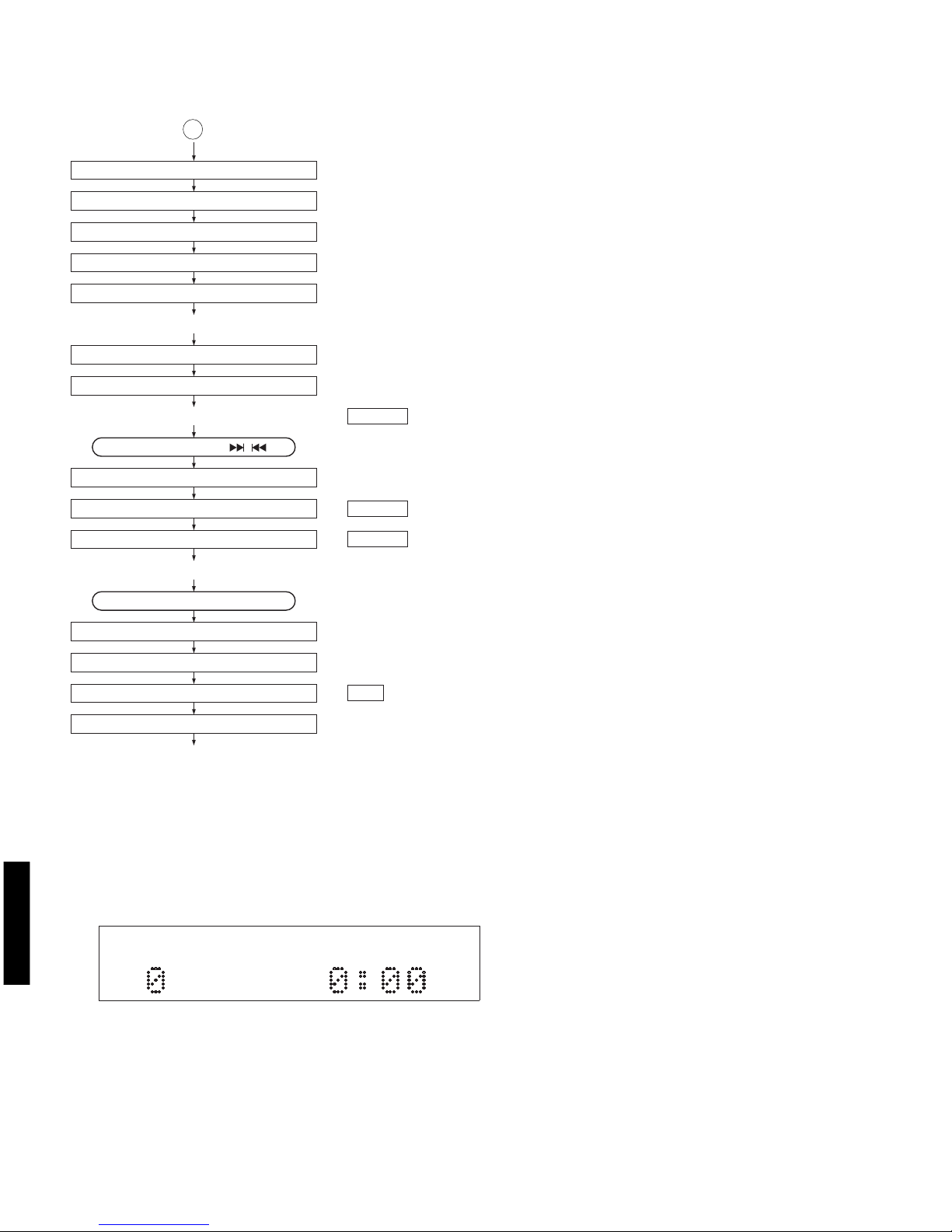
(2) Shown below are the panel key and remote control transmitter functions in the TEST mode.
●Function List of Panel keys Note) "Traverse servo" means the same as "feed servo".
PANEL KEY
OPEN/CLOSE
(SKIP/SEARCH)
(SKIP/SEARCH)
+10
1
2
3
4
5
6
7
8
9
0
FUNCTION
Tray open/close.
FOON, TRON, SPON, TVON(FEON).
All stop. (Focus, spindle, feed, laser, tray, etc.) Initializes FL display
Inner circumference traverse servo.
Outer circumference traverse servo.
Rotating the mode of coefficients. (Coefficient mode −−− Coefficient setting −−− product mode)
Pressing twice will set to the product mode.
Returns to product mode.
Auto adjustment mode 1 (TR-off set, FO-off set, FO-rough gain adjustment)
Auto adjustment mode 2 (TR-balance, TR-rough gain adjustment)
Auto adjustment mode 3 (FO-fine gain, TR-fine gain, FO-balance adjustment)
1 TRACK KICK (–) continuously (Coefficient set up mode : address down)
1 TRACK KICK (+) continuously (Coefficient set up mode : address up)
30 TRACK KICK (–) continuously (Coefficient set up mode : upper digit down)
30 TRACK KICK (+) continuously (Coefficient set up mode : upper digit up)
150 TRACK KICK (–) continuously (Coefficient set up mode : lower digit down)
150 TRACK KICK (+) continuously (Coefficient set up mode : lower digit up)
CUSTOM CODE = (79)x
KEY
OPEN/CLOSE
REPEAT S/F
TIME
INDEX
PROG
CLEAR
SPACE
0
1
2
3
4
5
6
7
8
9
+10
RANDOM
DIMMER
TAPE
SYNCHRO
PEAK
CODE
01
02
04
05
06
07
08
0A
0B
0C
0D
0F
10
11
12
13
14
15
16
17
18
19
1A
1B
1E
55
56
57
58
5D
FUNCTION
Tray open/close.
PLAY (FOON, TRON, TVON(FEON), SPON)
Inner circumference traverse servo.
Inner 10 tracks kick continuously.
Outer 10 tracks kick continuously.
Outer circumference traverse servo.
FOON, TROF (Enter focus search if focus servo is off.)
Checks FL display. (88 8888 --- goes out −−− All lamps.)
FOON, TROF, TVOF(FEOF) (Enter focus search if focus servo is off.)
Rotates or accelerates spindle.
Decelerates spindle. (checking EFM pattern and reflected STAT)
FOOF, TROF, TVOF(EFOF)
150 TRACK KICK (+) continuously (Coefficient set up mode : lower digit up)
Returns to product mode. (tray inoperative.)
Auto adjustment mode 1 (TR-off set, FO-off set, FO-rough gain adjustment)
Auto adjustment mode 2 (TR-balance, TR-rough gain adjustment)
Auto adjustment mode 3 (FO-fine gain, TR-fine gain, FO-balance adjustment)
1 TRACK KICK (–) continuously (Coefficient set up mode : address down)
1 TRACK KICK (+) continuously (Coefficient set up mode : address up)
30 TRACK KICK (–) continuously (Coefficient set up mode : upper digit down)
30 TRACK KICK (+) continuously (Coefficient set up mode : upper digit up)
150 TRACK KICK (–) continuously (Coefficient set up mode : lower digit down)
Rotating the mode of coefficients.
SPON (Spindle servo on.)
Checks FL display. (All lamps −−− 88 8888 −−− goes out.)
FOON, TROF, TVOF(EFOF) (Enter focus search if focus servo is off.)
All stop. (Focus, spindle, traverse, laser, tray, etc.)
Spindle free (off)
TV(Feed) REV
-
●Function List of Remote Control Transmitter

CDX-596
CDX-596
■
ERROR MESSAGE
(1) When operation is terminated in an abnormal condition (stop or open), pressing STOP on the remote control while
pressing STOP on the panel will set to the error message display enable mode.
(2) Shown below is an example of display. ("E-73" as an example)
9
(3) This function stays effective till the power is turned OFF. (It is cleared at OFF.)
(4) Listed in the table below are error messages.
ERROR MESSAGES
E–X0
E–X1
E–71
E–72
E–73
E–94
E–A5
E–X7
E–X8
Er r
DESCRIPTION
Data cannot be read after finishing search.
Data cannot be read during PLAY(X=0), PAUSE(X=3), or SCAN(X=2).
At the start, tracking servo is not effective.
At the start, spindle servo PLL is not effective.
At the start, data cannot be read.
Close switch does not work with tray closed.
Open switch does not work with tray open.
Traverse(Feed) inner switch does not work.
Recovery action fails after focus drop.
MN35511AL does not give response of SENSE, with resetting by the
unit’s microcomputer.
●Error Messages List
*No. for each state
(meaning of "X")
PLAY X="0"
SCAN X="2"
PAUSE X="3"
PEAK SEARCH X="4"
SEARCH X="5"
START X="7"
STOP X="8"
LOADING X="9"
OPEN X="–"
NO DISC X="C"
1) Error Code Troubleshooting
Error code X0 , X1 , 73 ...... Data cannot be read. Error codes 94 , A5 ..... Poor tray loading operation.
YES
NO
Does tray
operate when
OPEN/CLOSE key is
pressed?
Motor defective.
Control IC (IC2) defective.
Microcomputer defective.
Loading switch defective.
Poor Microcomputer
defective.
YES
NO
Is disc dirty or
scratched?
Pick-up position
Within disc range
Pick-up defective, Spindle system
defective (Motor fails to run, etc.).
Outermost
(on mirror
surface)
Check by using
another disc.
TRACKING
servo defective.
FEED servo defective.
Error code X7 ............. FEED operation defective.
(Limit switch fails)
YES
NO
Is forced
feed operation
available in TEST
mode?
FEED servo defective.
Microcomputer defective.
Y...Outward
T...Inward
Feed limit switch
defective.
Microcomputer defective.
Error code X8 ............ Focus drops.
YES
NO
Is disc dirty or
scratched?
Pick-up position
FOCUS servo defective.
Pick-up defective.
Within disc range
Outermost
(on mirror
surface)
Check by using
another disc.
TRACKING servo
defective.
FEED servo defective.

CDX-596
CDX-596
10
2) Troubleshooting from System Malfunctions
a) Tray fails to come out/go in.
NO
FLSW = "L"
NO
YES
YES
NO
YES
Tray starts to
move but stops.
Is output
available at LOADING
terminal?
Poor mechanism
operation.
Wire caught.
Loose gear, etc.
Motor defective.
Microcomputer or
LOADING IC (IC2)
defective.
Limit switch defective.
FEED servo system defective.
Microcomputer, IC1 or IC3 defective.
When tray fails to close completely
(when it stops midway)
[Corrective measure]
1) Turn ON the power and open the tray.
* If it failed to open (head and tray contacting each other),
open it after removing the chucking unit.
2) Turn OFF the power and force the tray to go in fully and
close.
3) With the power turned ON, open and close the tray to
check if the tray close completely.
YES
YES
NO
NO
NO
MUTING applied.
Is normal
IC3 or IC100 defective.
DAC IC(IC101)?
digital data input to DAC IC(IC101) defective.
Audio amplifier
(IC102,103) defeective.
MUTING circuit defective.
Microcomputer defective.
b) No sound generated, Sound cut during play.
( but time display advances properly)
FOCUS servo
system defective.
YES
Is FOCUS
lock done?
IC3defective.
Microcomputer defective.
YES
NO
Feed limit switch defective.
Does tray
load properly? NO
YES
Is pick-up at
innermost position? NO
Poor tray loading.
Jitter defective.
YES
Is EFMI signal
normal? NO
Spindle servo
system defective.
YES
Does spindle
motor run? NO
c) Operates as if no disc loaded. (although loaded)
NO
YES
NO
YES
Is disc dirty,
scratched or
warped?
Is disc or disc
stabilizer in contact with
mechanism?
Tracking servo system defective.
FEED servo system defective.
FOCUS servo system defective.
Pick-up defective.
Check by using a
known good disc.
Poor mechanism
accuracy.
Floating rubber/
spring deformed.
Pick-up connector
assembly caught.
d) Sound skips.
(Time display fails to advance properly)
YES
YES
NO
NO
Is disc dirty,
scratched or
warped?
Is TER
waveform normal?
IC3 defective.
Check by using a
known good disc.
Tracking servo system defective.
FEED servo system defective.
FOCUS servo system defective.
Pick-up defective.
e) No search provided. (Sound skipped after search)

CDX-596
CDX-596
■
DISPLAY DATA
11
V300 : 14-BT-56GN
●GRID ASSIGNMENT ●ANODE CONNECTION
&0 #6
PATTERN AREA
q#5
Note 1) F1, F2 ......... Filament
2) NP .............. No Pin 3) NX .............. No Extend pin
4) P1~P35....... Datum Line 5) 1G~14G...... Grid
6) IC ................ Internal Connection
●PIN CONNECTION
Pin No. 1 2 3456789101112131415161718192021222324252627282930
Connection F1 F1 NP 14G 13G 12G 11G 10G 9G 8G 7G 6G 5G 4G 3G 2G NX NX NX NX 1G IC P35 P34 P33 P32 P31 P30 P29 P28
Pin No. 31 32 33 34 35 36 37 38 39 40 41 42 43 44 45 46 47 48 49 50 51 52 53 54 55 56 57 58 59 60
Connection P27 P26 NP F2 F2 F2 F2 NP P25 P24 P23 P22 P21 P20 P19 P18 P17 P16 P15 P14 P13 NX NX NX NX P12 P11 P10 P9 P8
Pin No. 61 62 63 64 65 66 67 68 69 70
Connection P7 P6 P5 P4 P3 P2 P1 NP F1 F1

CDX-596
CDX-596
■IC DATA
IC100: YSZ914B-F
DAFC
4
14
10
15
11
SI0
INPUT
INPUT
SI1
3
PROBIT DELAY
LEVELDET COUNTER CALCULATOR
BIT SHIFT
DELAY
LEVELDET COUNTER CALCULATOR
BIT SHIFT
SO0
SO1
MUTE0
MUTE1
SO2
SO3
MUTE2
MUTE3
OUTPUT
OUTPUT
17
19
16
23
44 43 42 41 40 39 38 37 36 35 34
33
32
31
30
29
28
27
26
25
24
23
2221201918171615141312
11
10
9
8
7
6
5
4
3
2
1
VDD
VSS
SI1
SI0
SYNC/LR
BCKI
128Fs
VSS
VDD
MUTE0
SO0
RESET
LENG
PRO
ISM
KM0
TEST
KM1
FIX
VSS
VDD
MUTE3
OMOD1
OMOD0
GSEL1
GSEL0
FS1
FS0
IMOD2
IMOD1
IMOD0
VDD
VSS
VDD
VSS
SO1
MUTE1
MUTE2
SO2
WCKO
SO3
BCKO
VSS
VDD
12
.oNNIPEMANO/INOITCNUF.oNNIPEMANO/INOITCNUF
1DDVylppusrewoPV5+323ETUMO )etuM:H(langisetuM1hc
2SSVDNG42DDVylppusrewoPV5+
31ISI )3,2hc(NIatadlaireS52SSVDNG
40ISI )1,0hc(NIatadlaireS62XIFI FFO/NOedafssorC
5RL/CNYSI langis.cnyS721MKI lortnocesahpIKCB
6IKCBI )kcolcmetsyS(kcolctiB82TSETI )tseT:L(tseT
7SF821I langisSF821920MKI lortnoc.cnysemarF
8SSVDNG03MSII enilNInarofhcforebmuN
9DDVylppusrewoPV5+13ORPI lortnoctib-orP
010ETUMO )etuM:H(langisetuM0hc23GNELI tib-orpfohtgneldrowtupnI
110OSO TUOatadlaireS0hc33TESERIteseR
21DDVylppusrewoPV5+43SSVDNG
31SSVDNG53DDVylppusrewoPV5+
411OSO TUOatadlaireS1hc630DOMII tamrofenilNI511ETUMO )etuM:H(langisetuM1hc731DOMII
612ETUMO )etuM:H(langisetuM2hc832DOMII
712OSO TUOatadlaireS2hc930SFI lortnocetargnilpmaS
81OKCWO kcolcdrowlaireS041SFI
913OSO TUOatadlaireS3hc140LESGI lortnocniaggnitaolF
02OKCBO kcolctiblaireS241LESGI
12SSVDNG340DOMOI tamrofenilTUO
22DDVylppusrewoPV5+441DOMOI

CDX-596
CDX-596
IC3 : MN35511AL
Signal Process Controller (SPC) & D/A Converter
13
60 59 58 57 56 55 54 53 52 51 50 49 48 47 46 45 44 43 42 41
1 2 2 4 5 6 7 8 9 1011121314151617181920
40
39
38
37
36
35
34
33
32
31
30
29
28
27
26
25
24
23
22
21
61
62
63
64
65
66
67
68
69
70
71
72
73
74
75
76
77
78
79
80
BCLK
LRCK
SRDATA
DVDD1
DVSS1
TX
MCLK
MDATA
MLD
SENSE
/FLOCK
/TLOCK
BLKCK
SQCK
SUBQ
DMUTE
STAT
/RST
SMCK/FCLK
CLVS/FLAG6
VCOF2
AVSS1
OUT1C
OUT1D
OUT2D
OUT2C
AVDD1
DEMP0
CK384
IOSEL
/TEST
SBCK2
SUBC
SBCK
/CLDCK
IPFLAG
DEMP1/TEST2
SDATI
LRCKI
BCKI
VDD
X2
X1
VSS
XSEL
CRC
FLAG
PCK/RESY
EFM
AVSS2
AVDD2
VCOF
PLLF
DSLF
DRF
IREF
ARF
WVEL
PLAY/TRVSTOP
TOFS
LDON
BDO
/RFDET
TRCRS
OFT
VDET
RFENV
TE
FE
TBAL
FBAL
VREF
FOD
TRD
KICK
ECS
ECM
PC
TVD
TRV
60
17 58 59 56 19 49 69 8 7 9 44 46 45 47 48 52 53 67 62 15 14 20 68 73 72 74 75 13 55 70 78 80 79 77
57
4
5
18
71
32
33
34
37
35
39
38
36
10 43 41 40 11 12 30 31 28 27 22 25 42 29 26 21 16 1 3 223 24 6 76 54 51 63 64 66 65 50
61
VDD
VSS
DVDD1
DVSS1
/RST
/TEST
FE
TE
RFFNV
TRCRS
VDET
BDO
/RFDET
OPT
A/D CONVERTER
STAT
X1
X2
XSEL
SMCK/FCLK
VCOF
CK384
MDATA
MCLK
MLD
ARF
DRF
IREF
DSLF
PLLF
EFM
PCK/RESY
AVSS
SUBQ
SQCK
DEMPO
CRC
IOSEL
SUBC
SBCK2
SBCK
CLDCK
BLKCK
LRCKI
DEMP1/TEST2
SDATI
BCKI
CLVS/FLAG6
AVDD
INPUT PORT
SENSE
WVEL
TOFS
LDON
/FLOCK
/TLOCK
FBAL
TBAL
FOD
TVD
TRD
ECS
PLAY/TRVSTOP
VREF
KICK
TRV
DMUTE
BCLK
SRDATA
LRCK
PC
ECM
TX
IPFLAG
FLAG
AVSS2
OUT1C
OUT1D
OUT2C
OUT2D
AVDO2
SERVO
TIMING GENERATOR
VCO
TIMING
GENERATOR
PITCH CONTROL
MICRO COMPUTER
INTERFACE
SERVO
CPU
INTERPOLATION
SOFT MUTING
DIGITAL
ATTENUATION
OUTPUT
PORT D/A
CONVERTER
PEAK DETECT
AUTO CUE
CLV
SERVO DIGITAL
AUDIO
INTERFACE
16K
SRAM
CIRC ERROR CORRECTION
DEINTERLEAVE
EFM DEMODULATION
SYNC INTERPOLATION
SUBCODE DEMODULATION
DSL.PLLVCO SUBCODE
BUFFER
DIGITALDE-EMPHASIS
8 TIMES
OVER SAMPLING
DIGITALFILTER
PLLVCO2 VSOF2
DO
DAC
PEM
(L) PEM
(R)

CDX-596
CDX-596
14
.oNNIPEMANO/INOITCNUF.oNNIPEMANO/INOITCNUF
1KLCBCN14SFOTCN
2KCRLCN24YALPCN
3RDRSCN34LEVWCN
41DDVD
+
V5 44FRAIlangisFR
51SSVDDNG54FERII tnerrucecnerefeR
6XTO langisecafretnioidualatigiD64FERDILSDrofsaiB
7KLCMIkcolcUPC74FLSDO/ILSDrofretlifpooL
8ATADMIatadUPC84FLLPO/ILLProfretlifpooL
9DLMI langisdaolUPC94FOCV
+
V5
01ESNESOlangisesneS052DDVA
+
V5
11KCOLF/O langiswardovressucoF152SSVADNG
21KCOLT/O langiswardovresgnikcarT25MFECN
31KCKLBO kcolckcolbedoc-buS35KCPCN
41KCQSI kcolcQedoc-buS45GALFCN
51QBUSO langisedocQedoc-buS55CRCCN
61ETUMDIlangisetuM65LESXDNG
71TATSOlangissutatS75SSVDNG
81TSR/IlangisteseR851XI noitallicolatsyrC
91KLCF/KCMSCN952XO noitallicolatsyrC
026GALF/SVLCCN06DDV
+
V5
12VRTO langisdeefdecrofesrevarT162FOCVDNG
22DVTO langisevirdesrevarT261SSVADNG
32CPCN36C1TUOO langisC1MEP
42MCEO langisevirddecrofeldnipS46D1TUOO langisD1MEP
52SCEO langisevirdeldnipS56D2TUOO langisD2MEP
62KCIKOeslupkciK66C2TUOO langisC2MEP
72DRTO langisevirdgnikcarT761DDVA
+
V5
82DOFO langisevirdsucoF86OPMEDlangistcetedsisahpme-eD
92FERVO egatloVecnerefeR96483KCOCN
03LABFO langisecnalabsucoF07LESOI)H(tcelesedoM
13LABTO langisecnalabgnikcarT17TSET/)H(tesedomtseT
23EFI langisrorresucoF272KCBSCN
33ETI langisrorregnikcarT37CBUSCN
43VNEFRI langisepolevneFR47KCBSCN
53TEDVDNG57KCDLC/CN
63TFOI langiskcart-ffO67GALFPICN
73SRCRTI langisesolcgnikcarT77IPMEDDNG
83TEDFR/I tcetedlangisFR87ITADSCN
930DBI tcetedtodkcalB97IKCRLCN
04NODLO langisNOresaL08IKCBCN

CDX-596
CDX-596
IC300 : uPD78076GF-088
System Control
15
16-bit TIMER/
EVENT COUNTER
EVENT COUNTER1
TO0/P30
8-bit TIMER/
EVENT COUNTER2
EVENT COUNTER5
SERIAL
INTERFACE0
WATCHDOG TIMER
WATCH TIMER
INTERRUPT
CONTROL
V
PP
V
SS
V
DD
PORT0 P01-P03
P00
P04
P10-P17
P20-P27
P30-P37
P80, P81
P90-P97
PORT1
PORT2
PORT3
P40-P47
P50-P57
P60-P67
PORT4
PORT5
PORT6
PORT8
PORT9
PORT10
PORT11
P100-P107
P110-P117
AD0/P40—
AD7/P47
A0/P80—
A7/P87
A8/P50—
A15/P57
RD/P64
78K/0
CPU CORE
8-bit TIMER/
A/D CONVERTER
TI0/INTP0/P00
TI01/INTP1/P01
TO1/P31
TI1/P33
TO2/P32
TI2/P34
8-bit TIMER/
EVENT COUNTER6
8-bit TIMER/
TI5/TO5/P100
TI6/TO6/P101
SI0/SB0/P25
SO0/SB1/P26
SCK0/P27
SI1/P20
SO1/P21
SCK1/P22 SERIAL
INTERFACE1
AV
DD
ANI0/P10-
ANI7/P17
INTP0/TI0/P00—
INTP3/CI0/P03
EXTERNAL
ACCESS
BUZZER OUTPUT
CLOCK OUTPUT
CONTROL
PCL/P35
BUZ/P36
RESET
SYSTEM
CONTROL
PROM
RAM
X1
X2
XT1/P04
XT2
WR/P65
WAIT/P66
ASTB/P67
STB/P23
BUSY/P24
AV
REF
AV
SS
D/ACONVERTER
ANO0/P130
ANO1/P131
AV
REF1
AV
SS
P70-P74
PORT7
PORT12 P120-P127
PORT13 P130,P131
REAL-TIME
OUTPUT PORT RTP0/P120—
RTP7/P127
SERIAL
INTERFACE2
SI2/RxD/P70
SO2/TxD/P71
SCK2/ASCK/P72
P120/RTP0
P121/RTP1
P122/RTP2
P123/RTP3
P124/RTP4
P125/RTP5
P126/RTP6
P127/RTP7
V
PP
X2
X1
V
DD
XT2
XT1/P07
RESET
P00/INTP0/TI00
P01/INTP1/TI01
P02/INTP2
P03/INTP3
P04/INTP4
P05/INTP5
P06/INTP6
AV
DD
AV
REF0
P10/ANI0
P11/ANI1
P12/ANI2
P13/ANI3
P14/ANI4
P15/ANI5
1
2
3
4
5
6
7
8
9
10
11
12
13
14
15
16
17
18
19
20
21
22
23
24
25
26
27
28
29
30
80
79
78
77
76
75
74
73
72
71
70
69
68
67
66
65
64
63
62
61
60
59
58
57
56
55
54
53
52
51
P66/WAIT
P65/WR
P64/RD
P63
P62
P61
P60
P57/A15
P56/A14
V
SS
P55/A13
P54/A12
P53/A11
P52/A10
P51/A9
P50/A8
P47/AD7
P46/AD6
P45/AD5
P44/AD4
P43/AD3
P42/AD2
P41/AD1
P40/AD0
P87/A7
P86/A6
P85/A5
P84/A4
P83/A3
P82/A2
P96
P95
P94
P93
P92
P91
P90
P37
P36/BUZ
P35/PCL
P34/TI2
P33/TI1
P32/TO2
P31/TO1
P30/TO0
P103
P102
P101/TI6/TO6
P100/TI5/TO5
P67/ASTB
31 32 33 34 35 36 37 38 39 40 41 42 43 44 45 46 47 48 49 50
100
99 98 97 96 95 94 93 92 91 90 89 88 87 86 85 84 83 82 81
P16/ANI6
P17/ANI7
AV
SS
P130/ANO0
P131/ANO1
AV
REF1
P70/SI2/R
X
D
P71/SO2/T
X
D
P72/SCK2/ASCK
V
SS
P20/SI1
P21/SO1
P22/SCK1
P23/STB
P24/BUSY
P25/SI0/SB0
P26/SO0/SB1
P27/SCK0
P80/A0
P81/A1

CDX-596
CDX-596
16
NIP .oN EMAN O/INOITCNUF NIP .oN EMAN O/INOTICNUF
ECIVEDTIUCRICECIVEDTIUCRIC
10PTR/021PWSPOI hctiwstimilnepoyarT152A/28PKLB/O 1157CLroflangislortnoC
21PTR/12PWSLCI hctiwstimilesolcyarT253A/38POTSRCFAD
32PTR/221PCN354A/48PCN
43PTR/321PETUMO langisetumgolanA455A/58PFFODEEFO langisetumdeeF
54PTR/421PTSR/O langisteseR556A/68PCN
65PTR/521PETUMDO langisetumlatigiD657A/78PCN
76PTR/621PKCOLT/I langisovresgnikcarT750DA/04PCN
87PTR/721PKCOLF/I langisovressucoF851DA/14PCN
9V(CI
PP
)CIDNG952DA/24PCN
012X2XlanimretCSO063DA/34PCN
111X1XlanimretCSO164DA/44PCN
21DDVDDV
+
V5 265DA/54PCN
312TX2TXCN366DA/64PCN
4170P/1TX1TX
+
V5 467DA/74PCN
51TESERTESER/I langisteseR568A/05PCN
6100IT/0PTNI/00PMERI langisreviecerlortnocetomeR669A/15P3DKO
3–0slangistigidyeK
7110IT/1PTNI/10PKCKLBI kcolckcolbedocbuS7601A/25P2DKO
812PTNI/20PDELO langislortnocDEL8611A/35P1DKO
913PTNI/30PWSNWODCN9621A/45P0DKO
024PTNI/40PWSPUCN0731A/55PCN
125PTNI/50PWSLFI hctiwstimildeeF17V
SS
SSVDNG
226PTNI/60PKCOLC/IkcolC2741A/65PCN
32VA
DD
DDVA
+
V5 3751A/75PCN
42VA
0FER
0FERVADNG4706P4KI
4–0slangisnruterni-yeK
520INA/01PCN5716P3KI
621INA/11PCN6726P2KI
722INA/21PCN7736P1KI
823INA/31PCN87DR/46P0KI
924INA/41PADSO/IMORPEErofataD97RW/56PCN
035INA/51PLCSO MORPEErofkcolC08TIAW/66PCN
136INA/61PCN18BTSA/76PCN
237INA/71PCN285OT/5IT/001PCN
33VA
SS
SSVADNG386OT/6IT/101PCN
430ONA/031PSLC/NPOO langisesolC/nepO48201PCN
531ONA/131PLRTCGO langislortnocniaG58301PCN
63VA
1FER
2FERV
+
V5 680OT/03PCN
73DxR/2IS/07PQBUSI langisQedoc-buS781OT/13PCN
83DxT/2OS/17PTATSI langissutatS882OT/23PCN
93KCSA/KCS/27PKCQSO Qedoc-busrofkcolcretsigeR981IT/33PCN
04V
SS
SSVDNG092IT/43PCN
141IS/02PCBUSI langislairesedoc-buS19LCP/53PCN
241OS/12PCN29ZUB/63PCN
341KCS/22P2KCBSO kcolcedoc-buS3973PNATSO langisybdnatS
44BTS/32PDLMO ossecorp-µroflangisdaoLr4909P
)HotdexiF(
54YSUB/42PESNESI langisesneS5919P
640BS/0IS/52POSCN6929P
741BS/0OS/62PATADMO rossecorp-µrofataD7939P
840KCS/72PKLCMO rossecorp-µrofkcolC8949P
940A/08PSC/CN9959P
051A/18PECO 11757CLroflangiselbanepihC00169P

■
BLOCK DIAGRAM
17
CDX-596

ABCDE FGHI J
1
2
3
4
5
6
7
1918
■
PRINTED CIRCUIT BOARD
(Foil side)
#2 #3
FLSW
GND
FEED-
FEED+
SPDL-
SPDL+
CLOSE
GND
OPEN
LOADING-
LOADING+
KSM-213CCM
MAIN P.C.B. (1)
OPTICALPICK-UP
VC
E
A
C
GND
VR
FCS+
TRK-
VCC
D
B
F
LD
PD
TRK+
FCS-
AC
GND
AC
#200
AC
F2
F1
#201
To : MAIN (3)
To : MAIN (3)
OPTICALCOAXIAL
DIGITAL AUDIO OUT
LINE OUT
18
4
41
1
1
30 31
50
51
8081
100
2021
40
41
60 61
80
58
5
18
45
1
1
1
45
8
1112 2223
33
3444
14 15
28
IC101
30 15
1
1
1
17
14 8
7
148
18
36 19
14
IC2
IC1
IC100
To : MAIN (5)
R
GND
L
F1
VP
/BLK
CL
GND
LED
K0
K2
K4
KD2
KDO
F2
GND
CE
DI
REM
+5
K1
K3
KD3
KD1
To : MAIN (2)
IC3
IC300 Ref. No. Location
D100
D101
D200
D201
D202
D203
D204
D205
D206
D207
D209
D210
D211
D212
D213
D214
D215
D216
D217
D218
D219
D221
D222
D223
Q1
Q3
Q4
Q5
Q100
Q101
Q102
Q103
Q201
Q202
Q203
Q204
Q205
Q300
IC1
IC2
IC3
IC100
IC101
IC102
IC103
IC104
IC105
IC200
IC300
IC301
I3
H3
G5
F5
F5
F6
F5
C6
D5
D6
D5
F5
D5
D6
D6
D6
D6
D3
D6
D7
C6
F6
G4
G4
C4
E3
D2
G5
F6
H6
G6
G6
F5
E5
E6
D3
C6
F2
D4
E3
F4
H3
H4
G5
H5
H2
D6
E5
G3
G4
• Semiconductor Location

2120
■
PRINTED CIRCUIT BOARD
(Foil side)
ABCDE FGHI J
1
2
3
4
5
6
7
MAIN P.C.B. (3)
MAIN P.C.B. (2)
MAIN P.C.B. (4)
MAIN P.C.B. (5)
BE
WH
AC
IN W200
#200
#201
WH
BE
To :
MAIN (1)
To :
MAIN (1) To :
MAIN (1)
AC
GND
AC
AC
F2
F1
L
GND
R
PHONES
POWER
(STOP) (PLAY)
OUTPUT LEVEL STOP/SEARCH 0987654321+10
VC VO
GOPEN/CLOSE
69 70
241621
32
3435
37 39 51
1
64
1617
32
33
48 49
56 6736
1
IC302
KD0
KD2
K4
K2
K0
LED
GND
CL
/BLK
VP
F1
KD1
KD3
K3
K1
+5V
REM
DI
CE
GND
F2
To : MAIN (1)
Ref. No. Location
D300
D301
D302
D303
D304
IC302
H2
D2
D2
C2
C2
F2
•Semiconductor Location
-
+
Table of contents
Other Yamaha CD Player manuals

Yamaha
Yamaha DVD-S1700B User manual

Yamaha
Yamaha CD-S3000 User guide

Yamaha
Yamaha DVD-CX1 User manual

Yamaha
Yamaha CDX-993 User manual

Yamaha
Yamaha VCD-120K User manual

Yamaha
Yamaha DRC-20 User manual

Yamaha
Yamaha DVD-S1700 User manual

Yamaha
Yamaha CDX-700U User manual

Yamaha
Yamaha CDX-820 User manual

Yamaha
Yamaha CDC-735 User manual

Yamaha
Yamaha CDX-450 User manual

Yamaha
Yamaha CD-S303 User manual

Yamaha
Yamaha CDM-900 User manual

Yamaha
Yamaha CD-450 User manual

Yamaha
Yamaha CDX-397 User manual

Yamaha
Yamaha CD-NT670 User manual

Yamaha
Yamaha CDX-410U User manual

Yamaha
Yamaha CDC-755 User manual

Yamaha
Yamaha CD-X1 User manual

Yamaha
Yamaha CDC-697 User manual