CLM920 Development Board User Manual
Shanghai Yuge Information Technology co., LTD
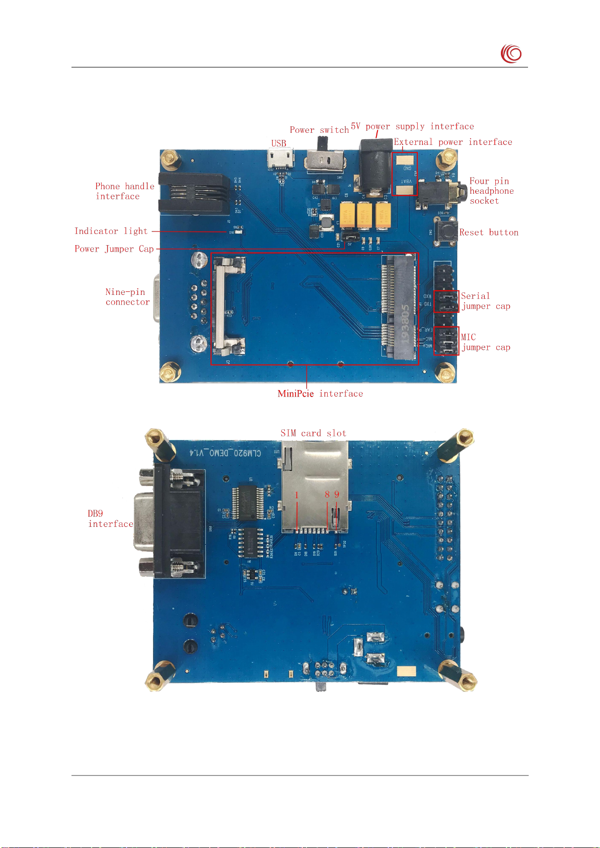
Development board basic interface debugging overview:
1. Support one 5V DC input interface (using 5V power supply, you can set the power switch
to the side of the 5V power supply interface)
2. Support one USB 2.0 interface (Using USB to directly power the development board, you
can turn the switch to the USB side)
3. Support one 3.7V DC input interface (connect the pads VBAT and GND to the 3.7V
4. One SIM card holder, U11 is a SIM card holder, the big card self-playing card holder
supports 3.0V or 1.8V USIM / SIM, and also supports the SIM card hot-swap function
(when inserting the SIM, the notch of the SIM card faces inward and the card chip faces
5. Supports one 9-pin serial port (module default baud rate 115200)
6. Supports one 4-way headphone jack
7. Support one-way phone handle interface (for debugging analog voice)
8. One LED indicator (module status D10 is indicator, red)
9. J1 is a 52PIN MINIPCI interface, which can be connected to the CLM920 Mini PCIE
series module for testing and debugging.
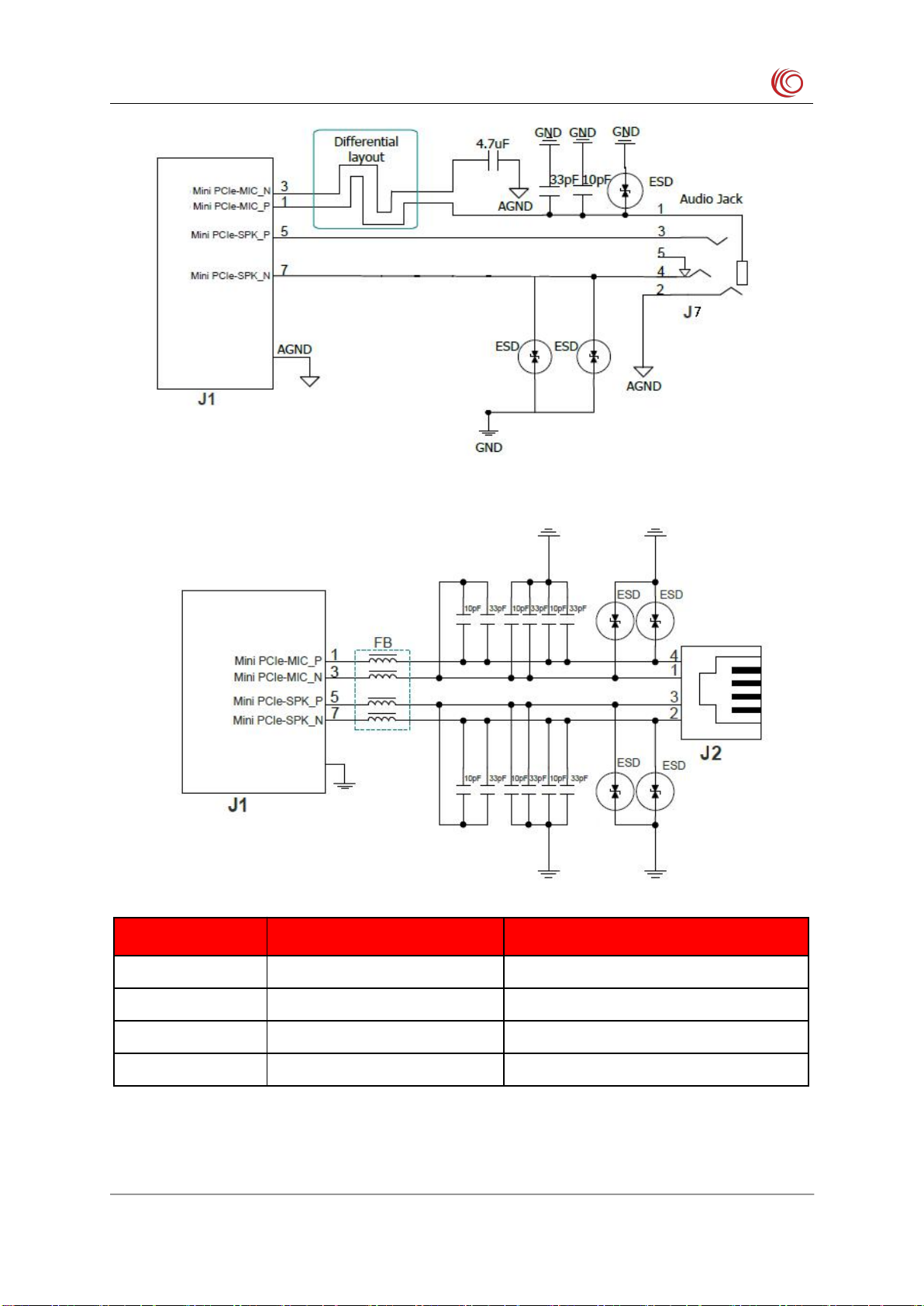
10. Supports 2 * 10 pin headers and some test interfaces for module analog voice and
11. J12 is a power jumper. It does not provide USB and 5V external power supply after
disconnection. It can only use 3.7V for power supply outside the wiring harness.
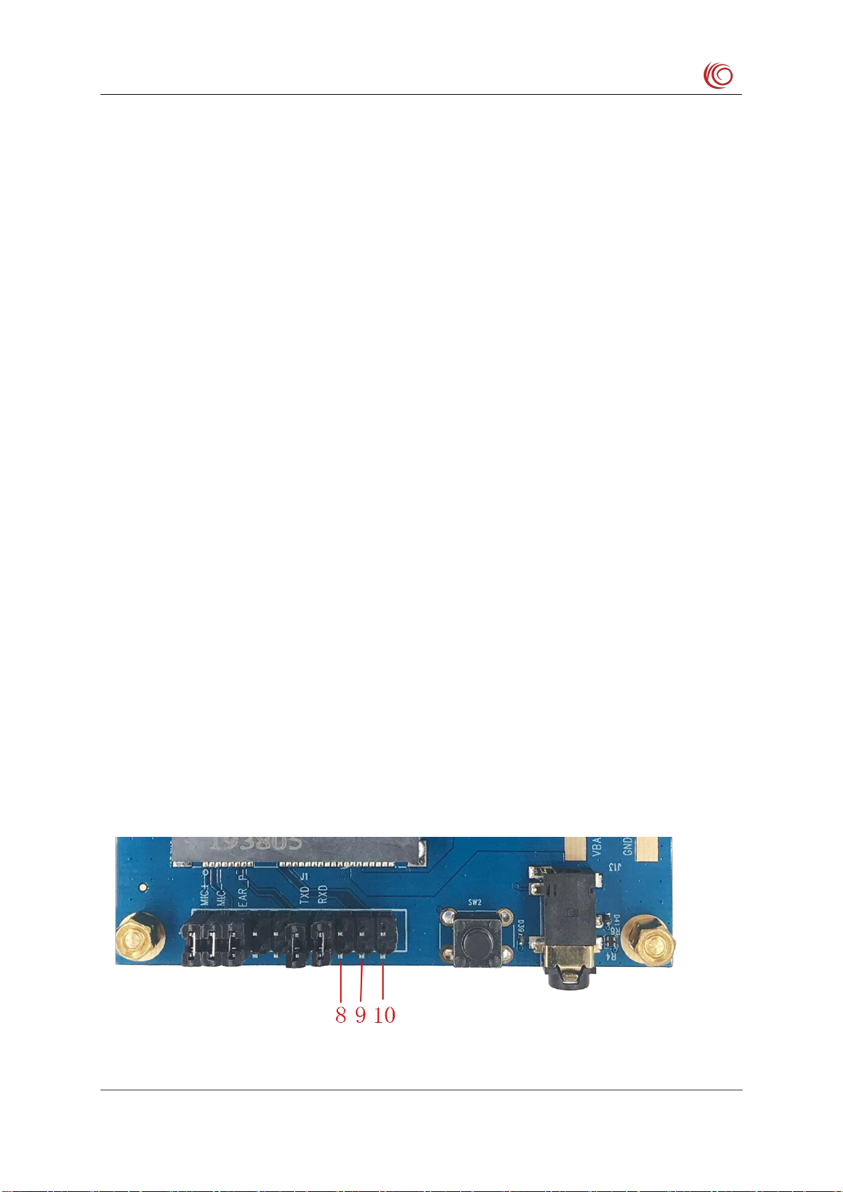
12. Pins 8, 9, and 10 of J10 correspond to the three pins of J1, 32, 20, and 19. These pins are
connected for the convenience of measuring and debugging the corresponding functions.