Zynq ZedBoard User manual

ZedBoard
Zynq™ Evaluation and Development
Hardware User’s Guide
Version 1.1
August 1st, 2012

1-Aug-2012
1
Revision History
Rev date
Rev #
Reason for change
8/1/12
1.0
Initial ZedBoard User’s Guide
8/2/12
1.1
Mapped Configuration Mode Table to match ZedBoard layout

1-Aug-2012
2
Table of Contents
1INTRODUCTION.................................................................................................................................. 3
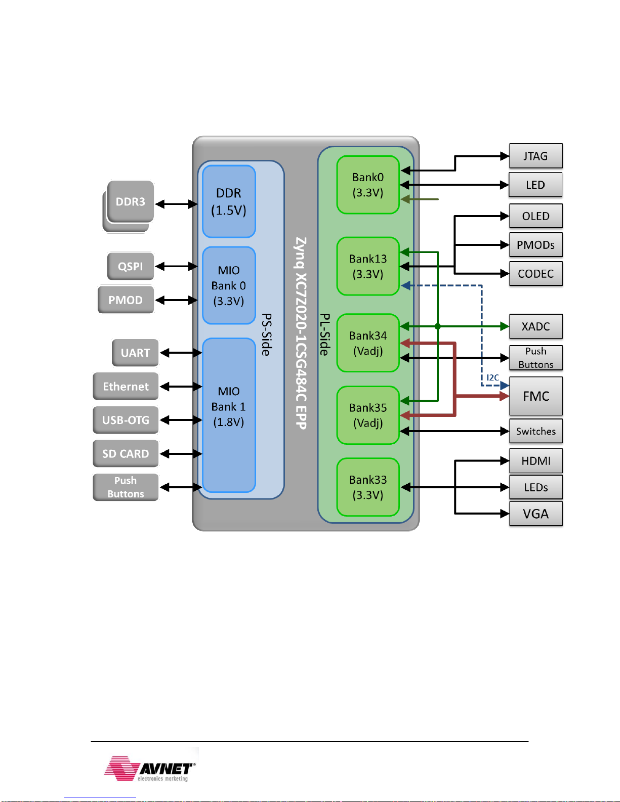
1.1 ZYNQ BANK PIN ASSIGNMENTS ...................................................................................................... 5
2FUNCTIONAL DESCRIPTION............................................................................................................ 6
2.1 EPP................................................................................................................................................. 6
2.2 MEMORY......................................................................................................................................... 6
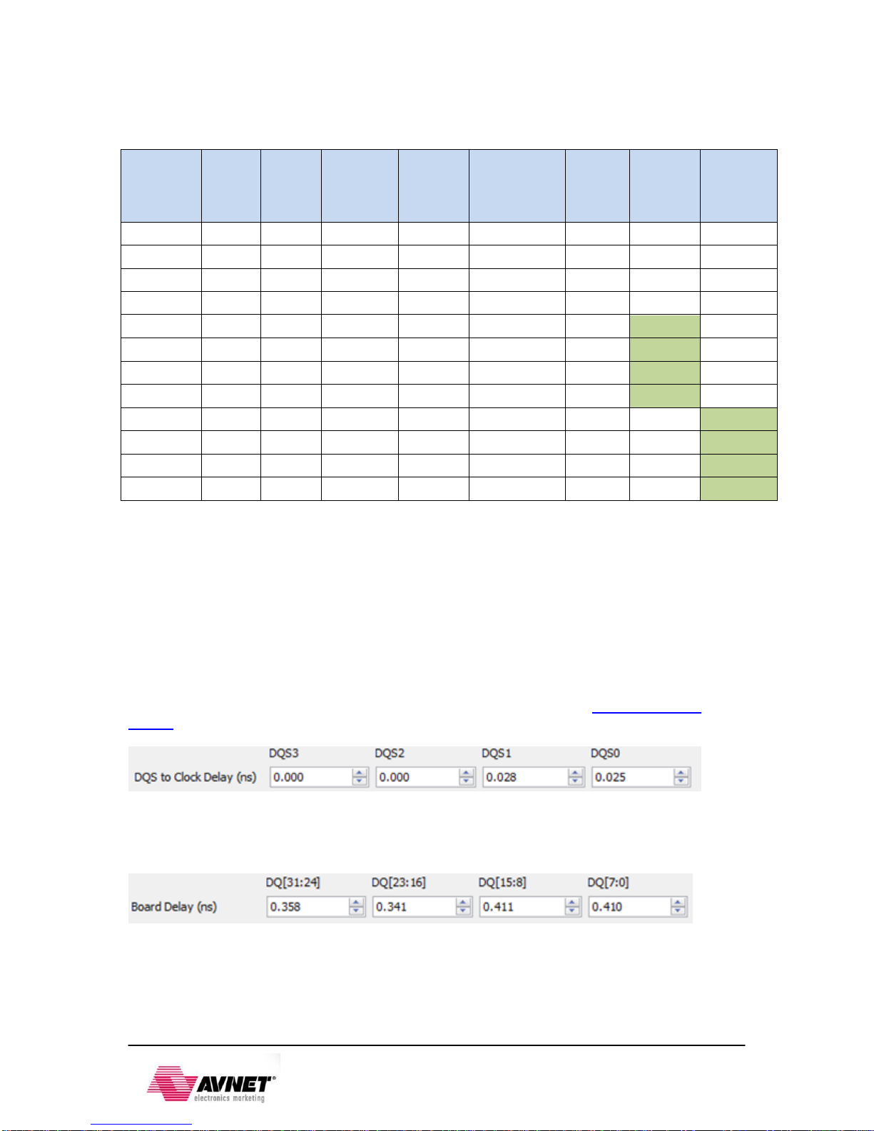
2.2.1 DDR3...................................................................................................................................... 6
2.2.2 SPI Flash ................................................................................................................................ 9
2.2.3 SD Card Interface..................................................................................................................11
2.3 USB ...............................................................................................................................................12
2.3.1 USB OTG...............................................................................................................................12
2.3.2 USB-to-UART Bridge ............................................................................................................12
2.3.3 USB-JTAG.............................................................................................................................13
2.3.4 USB circuit protection...........................................................................................................14
2.4 DISPLAY AND AUDIO......................................................................................................................14
2.4.1 HDMI Output.........................................................................................................................14
2.4.2 VGA Connector......................................................................................................................17
2.4.3 I2S Audio Codec....................................................................................................................18
2.4.4 OLED.....................................................................................................................................19
2.5 CLOCK SOURCES.............................................................................................................................19
2.6 RESET SOURCES .............................................................................................................................19
2.6.1 Power
‐
on Reset (PS_POR_B)................................................................................................19
2.6.2 Program Push Button Switch.................................................................................................20
2.6.3 Processor Subsystem Reset....................................................................................................20
2.7 USER I/O........................................................................................................................................20
2.7.1 User Push Buttons .................................................................................................................20
2.7.2 User DIP Switches.................................................................................................................20
2.7.3 User LEDs .............................................................................................................................21
2.8 10/100/1000 ETHERNET PHY ........................................................................................................21
2.9 EXPANSION HEADERS ....................................................................................................................22
2.9.1 LPC FMC Connector.............................................................................................................22
2.9.2 Digilent Pmod™ Compatible Headers (2x6).........................................................................23
2.9.3 Agile Mixed Signaling (AMS) Connector, J2.........................................................................24
2.10 CONFIGURATION MODES................................................................................................................27
2.10.1 JTAG......................................................................................................................................28
2.11 POWER ...........................................................................................................................................29
2.11.1 Primary Power Input.............................................................................................................29
2.11.2 On/Off Switch ........................................................................................................................29
2.11.3 Regulators..............................................................................................................................29
2.11.4 Sequencing.............................................................................................................................30
2.11.5 Power Good LED ..................................................................................................................31
2.11.6 Power Estimation ..................................................................................................................31
2.11.7 Testing ...................................................................................................................................31
2.11.8 Probes....................................................................................................................................32
3ZYNQ EPP BANKS..............................................................................................................................33
3.1 ZYNQ EPP BANK VOLTAGES..........................................................................................................34
4JUMPER SETTINGS............................................................................................................................35
5MECHANICAL ....................................................................................................................................37

1-Aug-2012
3
1 Introduction
The ZedBoard is an evaluation and development board based on the Xilinx Zynq-7000 Extensible
Processing Platform. Combining a dual Corex-A9 Processing System (PS) with 85,000 Series-7
Programmable Logic (PL) cells, the Zynq-7000 EPP can be targeted for broad use in many
applications. The ZedBoard’s robust mix of on-board peripherals and expansion capabilities
make it an ideal platform for both novice and experienced designers. The features provided by
the ZedBoard consist of:
Xilinx® XC7Z020-1CSG484CES EPP
oPrimary configuration = QSPI Flash
oAuxiliary configuration options
Cascaded JTAG
SD Card
Memory
o512 MB DDR3 (128M x 32)
o256 Mb QSPI Flash
Interfaces
oUSB-JTAG Programming using Digilent SMT1-equivalent circuit
Accesses PL JTAG
PS JTAG pins connected through PS Pmod
o10/100/1G Ethernet
oUSB OTG 2.0
oSD Card
oUSB 2.0 FS USB-UART bridge
oFive Digilent Pmod™ compatible headers (2x6) (1 PS, 4 PL)
oOne LPC FMC
oOne AMS Header
oTwo Reset Buttons (1 PS, 1 PL)
oSeven Push Buttons (2 PS, 5 PL)
oEight dip/slide switches (PL)
oNine User LEDs (1 PS, 8 PL)
oDONE LED (PL)
On-board Oscillators
o33.333 MHz (PS)
o100 MHz (PL)
Display/Audio
oHDMI Output
oVGA (12-bit Color)
o128x32 OLED Display
oAudio Line-in, Line-out, headphone, microphone
Power
oOn/Off Switch
o12V @ 5A AC/DC regulator
Software
oISE® WebPACK Design Software
oLicense voucher for ChipScope™ Pro locked to XC7Z020

1-Aug-2012
4
ZYNQ XC7Z020-CSG484
DDR3
MIC In
Line In
Line Out
HdPhn Out
32
Pmods
QSPI 7
Pmod
Flash
8
14
Gbit
Enet
12
USB
OTG
8
SD
2
1 LED,
2 buttons
USB
Cont
USB
UART
3
71
4USB
Cont
Clk
FMC-LPC
GPIO (8 LEDs,
8 slide switches,
5 pushbuttons)
Type A
HDMI Out
82
21
8
27
10
5
VGA (12-
bit color)
128x32 OLED
PHY
1
1
33Mhz
Reset
Primary JTAG
512Mbyte
DDR3 (x32)
MIOPS
PL
1PROG
Display
DDR
PS_RST
JTAG
PS_CLK
<User
Select>
ENET/
MDIO
USBOTG
SD
USBUART
PS_GPIO
QSPI
I2S/ACD
GPIO
FMC
PMOD
HDMI
VGA
OLED
PROG
PHY
HDMI
transmitter
I2S Audio
Codec
XADC
8
GPIO/VP/VN
1DONE LEDDONE
Figure 1 –ZedBoard Block Diagram

1-Aug-2012
5
1.1 Zynq Bank Pin Assignments
The following figure shows the Zynq bank pin assignments on the ZedBoard followed by a table
that shows the detailed I/O connections. .
Figure 2 - Zynq Z7020 CSG484 Bank Assignments

1-Aug-2012
6
2 Functional Description
2.1 EPP
The ZedBoard features a Xilinx Zynq XC7Z020-1CSG484 EPP. The initial ZedBoards ship with
Engineering Sample "CES" grade silicon. Later shipments will eventually switch to production "C"
grade silicon once they become available. The EPP part markings indicate the silicon grade.
2.2 Memory
Zynq contains a hardened PS memory interface unit. The memory interface unit includes a
dynamic memory controller and static memory interface modules.
2.2.1 DDR3
The ZedBoard includes two Micron MT41K128M16HA-15E:D DDR3 memory components
creating a 32-bit interface. The DDR3 is connected to the hard memory controller in the
Processor Subsystem (PS) as outlined in the Zynq datasheet.
The multi-protocol DDR memory controller is configured for 32-bit wide accesses to a 512 MB
address space. The PS incorporates both the DDR controller and the associated PHY, including
its own set of dedicated I/Os. DDR3 memory interface speeds up to 533MHz (1066Mbs) are
supported.
The DDR3 uses 1.5V SSTL-compatible inputs. DDR3 Termination is utilized on the ZedBoard.
The EPP and DDR3 have been placed close together keeping traces short and matched.
DDR3 on the PS was routed with 40 ohm trace impedance for single-ended signals, and DCI
resistors (VRP/VRN) as well as differential clocks set to 80 ohms. Each DDR3 chip needs its
own 240-ohm pull-down on ZQ.
DDR-VDDQ is set to 1.5V to support the DDR3 devices selected. DDR-VTT is the termination
voltage which is ½ DDR-VDDQ. DDR-VREF is a separate buffered output that is equal to ½
nominal DDR-VDDQ. The DDR-VREF is isolated to provide a cleaner reference for the DDR
level transitions.

1-Aug-2012
7
The PCB design guidelines outlined in Zynq datasheet must be followed for trace matching, etc.
Table 1 - DDR3 Connections
Signal Name
Description
Zynq EPP pin
DDR3 pin
DDR_CK_P
Differential clock
output
N4
J7
DDR_CK_N
Differential clock
output
N5
K7
DDR_CKE
Clock enable
V3
K9
DDR_CS_B
Chip select
P6
L2
DDR_RAS_B
RAS row address
select
R5
J3
DDR_CAS_B
RAS column address
select
P3
K3
DDR_WE_B
Write enable
R4
L3
DDR_BA[2:0]
Bank address
PS_DDR_BA[2:0]
BA[2:0]
DDR_A[14:0]
Address
PS_DDR_A[14:0]
A[14:0]
DDR_ODT
Output dynamic
termination
P5
K1
DDR_RESET_B
Reset
F3
T2
DDR_DQ[31:0]
I/O Data
PS_DDR_[31:0]
DDR3_DQ pins
DDR_DM[3:0]
Data mask
PS_DDR_DM[3:0]
LDM/UDM x2
DDR_DQS_P[3:0]
I/O Differential data
strobe
PS_DDR_DQS_P[3:0]
UDQS/LDQS
DDR_DQS_N[3:0]
I/O Differential data
strobe
PS_DDR_DQS_N[3:0]
UDQS#/LDQS#
DDR_VRP
I/O Used to calibrate
input termination
N7
N/A
DDR_VRN
I/O Used to calibrate
input termination
M7
N/A
DDR_VREF[1:0]
I/O Reference
voltage
H7, P7
H1
For best DDR3 performance, DRAM training is enabled for write leveling, read gate, and read
data eye options in the PS Configuration Tool in Xilinx Platform Studio (XPS). The PS
Configuration tools’ Memory Configuration Wizard contains two entries to allow for DQS to Clock
Delay and Board Delay information to be specified for each of the four byte lanes. These
parameters are specific to every PCB design. Xilinx Answer Record 46778 provides a tool for
calculating these parameters by a printed circuit board design engineers. The Excel worksheet
file ar46778_board_delay_calc.xlsx included in the answer record provides instructions in the
worksheet for calculating these board training details based upon specific trace lengths for certain
DDR3 signals. Using the information from the trace length reports pertaining to the DDR3
interface for ZedBoard these delay values can be recreated by following the directions found in
the Excel worksheet.
The PCB lengths are contained in the ZedBoard PCB trace length reports. The DQS to CLK
Delay and Board Delay values are calculated specific to the ZedBoard memory interface PCB
design. The AR46778 worksheet allows for up to 4 memory devices to be configured for DDR3
4x8 flyby topology. Note that ZedBoard is configured for DDR3 2x16 flyby routing topology. The
first two clock trace midpoint values (CLK0 and CLK1) are used to represent the Micron device
electrically nearest to 7Z020 (IC26) and the second two clock trace midpoint values (CLK2 and

1-Aug-2012
8
CLK3) are used to represent the Micron device electrically furthest from 7Z020 (IC25). The
worksheet calculation results are shown in the following table.
Table 2 - DDR3 Worksheet Calculations
Pin Group
Length
(mm)
Length
(mils)
Package
Length
(mils)
Total
Length
(mils)
Propagation
Delay
(ps/inch)
Total
Delay
(ns)
DQS to
CLK
Delay
(ns)
Board
Delay
(ns)
CLK0
55.77
2195.9
470
2665.9
160
0.427
CLK1
55.77
2195.9
470
2665.9
160
0.427
CLK2
41.43
1631.1
470
2101.1
160
0.336
CLK3
41.43
1631.1
470
2101.1
160
0.336
DQS0
51.00
2008.0
504
2512.0
160
0.402
0.025
DQS1
50.77
1998.8
495
2493.8
160
0.399
0.028
DQS2
41.59
1637.6
520
2157.6
160
0.345
-0.009
DQS3
41.90
1649.4
835
2484.4
160
0.398
-0.061
DQ[7:0]
50.63
1993.3
465
2458.3
160
0.393
0.410
DQ[15:8]
50.71
1996.4
480
2476.4
160
0.396
0.411
DQ[23:16]
40.89
1609.9
550
2159.9
160
0.346
0.341
DQ[31:24]
40.58
1597.8
780
2377.8
160
0.380
0.358
The DQS to CLK Delay fields in the PS7 DDR Configuration window should be populated using
the corresponding values from the previous table.
The configuration fields of the tool may not allow you to input a negative delay value, this is a
known problem with the 14.1 tools and scheduled for correction in the 14.2 tools release. In the
case of DQS2 and DQS3 fields for DQS to CLK Delay, simply enter a value of zero rather than
the negative delay values. This is an acceptable workaround since the calculated values are
relatively close to zero and the values provided in these fields are used as initial values for the
read/write training for DDR3. Keep in mind for LPDDR2 there is no write leveling, and for DDR2
there is no training whatsoever. In these memory use cases, the accuracy of the trace length info
is more important. This is covered in further detail in section 10.6.8 of the Xilinx Zynq TRM,
UG585.
Figure 3 - DQS to Clock Delay Settings
The Board Delay fields in the PS7 DDR Configuration window should be populated using the
corresponding values from the table above.
Figure 4 - DDR3 Board Delay Settings

1-Aug-2012
9
2.2.2 SPI Flash
The ZedBoard features a 4-bit SPI (quad-SPI) serial NOR flash. The Spansion S25FL256S is
used on this board. The Multi-I/O SPI Flash memory is used to provide non-volatile code, and
data storage. It can be used to initialize the PS subsystem as well as configure the PL
subsystem (bitstream). Spansion provides Spansion Flash File System (FFS) for use after
booting the Zynq EPP.
The relevant device attributes are:
256Mbit
x1, x2, and x4 support
Speeds up to 104 MHz, supporting Zynq configuration rates @ 100 MHz
oIn Quad-SPI mode, this translates to 400Mbs
Powered from 3.3V
The SPI Flash connects to the EPP supporting up to Quad-I/O SPI interface. This requires
connection to specific pins in MIO Bank 0/500, specifically MIO[1:6,8] as outlined in the Zynq
datasheet. Quad-SPI feedback mode is used, thus qspi_sclk_fb_out/MIO[8] is connected to a
20K pull-up resistor to 3.3V. This allows a QSPI clock frequency greater than FQSPICLK2.
Note: Zynq only supports 24-bit addressing, however the full capacity of the 256Mb Flash can be
accessed via internal bank switching. As of now the S25FL256S is not supported in iMPACT.
Note: 14.x is required for in-direct QSPI Flash Programming.
Table 3 –QSPI Flash Pin Assignment and Definitions
Signal Name
Description
Zynq EPP Pin
QSPI Pin
DQ0
Data0
A2 (Bank MIO0/500)
5
DQ1
Data1
F6 (MIO Bank 0/500)
2
DQ2
Data2
E4 (MIO Bank 0/500)
3
DQ3
Data3
A3 (MIO Bank 0/500)
7
SCK
Serial Data Clock
A4 (MIO Bank 0/500)
6
CS
Chip Select
A1 (MIO Bank 0/500)
1
FB Clock
QSPI Feedback
E5 (MIO Bank 0/500)
N/C
Note: The QSPI data and clock pins are shared with the Boot Mode jumpers.

1-Aug-2012
10
Two packages can be used on the ZedBoard; SO-16 and WSON. For the WSON package,
there is a heat sink slug under the package that is not connected to any signal on the PCB.
Figure 5 - Overlying Packages for SPI Flash

1-Aug-2012
11
2.2.3 SD Card Interface
The Zynq PS SD/SDIO peripheral controls communication with the ZedBoard SD Card (A 4GB
Class 4 card is included in the ZedBoard kit.) The SD card can be used for non-volatile external
memory storage as well as booting the Zynq EPP. PS peripheral sd0 is connected through Bank
1/501 MIO[40-47], including, Card Detect and Write Protect.
The SD Card is a 3.3V interface but is connected through MIO Bank 1/501 (1.8V). Therefore, a
TI TXS02612 level shifter performs this translation. The TXS02612 is a 2-port SDIO port
expander with level translation. ZedBoard only makes use of one of these parts. TI offered an
alternative TXS0206 device, but the 0.4mm pitch of that device’s packaging was too fine for our
manufacturer.
Based on the Zynq TRM, host mode is the only mode supported.
The ZedBoard SD Card is connected through a 9-pin standard SD card connector, J12, TE
2041021-1. A Class 4 card or better is recommended.
Note: To use the SD Card, JP6 must be shorted.
Figure 6 - SD Card Interface
Table 4 –SD Card Pin Assignment and Definitions
Signal
Name
Description
Zynq EPP Pin
Level Shift
Pin
SD Card Pin
CLK
Clock
E14 (MIO Bank 1/501)
Pass-Thru
5
CMD
Command
C8 ((MIO Bank 1/501)
Pass-Thru
2
Data[3:0]
Data
MIO Bank 1/501
D0: D8
D1: B11
D2: E13
D3: B9
Pass-Thru
Data Pins
7
8
9
1
CD
Card Detect
B10 (MIO Bank 1/501)
Pass-Thru
CD
WP
Write Protect
D12 ((MIO Bank 1/501)
Pass-Thru
WP

1-Aug-2012
12
2.3 USB
2.3.1 USB OTG
ZedBoard implements one of the two available PS USB OTG interfaces. An external PHY with
an 8-bit ULPI interface is required. A TI TUSB1210 Standalone USB Transceiver Chip is used as
the PHY. The PHY features a complete HS-USB Physical Front-End supporting speeds of up to
480Mbs. This part is available in a 32-pin QFN package. VCCio for this device is 1.8V and
cannot be connected through level shifters. The PHY is connected to MIO Bank 1/501, which is
powered at 1.8V. Additionally the USB chip must clock the ULPI interface which requires an
oscillator. A Fox XPRESSO oscillator (767-26-31) is used on ZedBoard.
The external USB interface connects through a TE 1981584-1.
The usb0 peripheral is used on the PS, connected through MIO[28-39] in MIO Bank 1/501.
This USB port will not power the board. However, ZedBoard provides 5V when in Host or OTG
modes. REFCLK pin of TUSB1210 is tied to ground as the EPP will drive the CLOCK input of this
part.
Table 5 - USB OTG Pin Assignment and Definitions
Signal Name
Description
Zynq EPP Pin
TUSB121
0 Pin
USB
Conn Pin
OTG_Data[8:0]
USB Data lines
MIO Bank 1/501
Data[7:0]
N/C
OTG_CLOCK
USB Clock
MIO Bank 1/501
26
N/C
OTG_DIR
ULPI DIR output signal
MIO Bank 1/501
31
N/C
OTG_STP
ULPI STP input signal
MIO Bank 1/501
29
N/C
OTG_NXT
ULPI NXT output signal
MIO Bank 1/501
2
N/C
OTG_CS
USB Chip Select
11
N/C
DP
DP pin of USB Connector
N/C
18
2
DM
DM pin of USB Connector
N/C
19
3
ID
Identification pin of the USB
connector
N/C
23
4
OTG_RESET_B
Reset
MIO Bank 1/501
27
N/C
OTG_VBUS_OC
VBus Output Control
Bank 34
L16
TPS2051
See the Jumper Settings section for configuring the USB interface for Host, Device and OTG
mode. The jumpers control the Vbus supply as well.
2.3.2 USB-to-UART Bridge
The ZedBoard implements a USB-to-UART bridge connected to a PS UART peripheral. A
Cypress CY7C64225 USB-to-UART Bridge device allows connection to a host computer. The
USB/UART device connects to the USB Micro B connector, J14, (TE 1981584-1) on the board.
Only basic TXD/RXD connection is implemented. If flow control is required this can be added
through Extended MIO on a PL-Pmod™.
Cypress provides royalty-free Virtual COM Port (VCP) drivers which permit the CY7C64225 USB-
to-UART bridge to appear as a COM port to host computer communications application software
(for example, HyperTerm or TeraTerm). Please refer to the CY7C64225 Setup Guide posted on
zedboard.org for detailed instructions for installing the driver.
The UART 1 Zynq PS peripheral is accessed through MIO[48:49] in MIO Bank 1/501 (1.8V).
Since the CY7C64225 device requires either 3.3V or 5V signaling, a TI TXS0102 level shifter is
used to level shift between 3.3V and 1.8V.

1-Aug-2012
13
This USB port will not power the board. Therefore, Vbus needs to be connected to 3.3V though a
1KΩ series resistor. The Wake pin, pin 22, connects to GND. A 24Ω series resistor was placed
on each of the data lines, D+ and D-.
Table 6 –CY7C6 Connections
EPP Pin
UART Function in
EPP
Schematic Net
Name
CY7C6 Pin
UART Function in
CY7C64225
D11 (MIO
Bank 1/501)
TX, data out
USB_1_RXD
23
RXD, data in
C14 (MIO
Bank 1/501)
RX, data in
USB_1_TXD
4
TXD, data out
Figure 7 –USB-UART Bridge Interface
2.3.3 USB-JTAG
The ZedBoard provides JTAG functionality based on the Digilent USB High Speed JTAG Module,
SMT1 device. This USB-JTAG circuitry is fully supported and integrated into Xilinx ISE tools,
including iMPACT, ChipScope, and SDK Debugger. Designers who want to re-use this circuit on
their board can do so by acquiring these modules from Avnet.
http://www.em.avnet.com/en-us/design/drc/Pages/Digilent-JTAG-SMT1-Surface-Mount-
Programming-Module.aspx
The JTAG is available through a Micro B USB connector, J17, TE 1981568-1.TCK has a series
termination resistor, 20-30Ω, to prevent signal integrity issues.
For the JTAG Chain setup, please refer to the Configuration section.

1-Aug-2012
14
2.3.4 USB circuit protection
All USB data lines, D+/-, are protected with a TE SESD0402Q2UG-0020-090.
Figure 8 –ESD Protection
2.4 Display and Audio
2.4.1 HDMI Output
An Analog Devices ADV7511 HDMI Transmitter provides a digital video interface to the
ZedBoard. This 225MHz transmitter is HDMI 1.4- and DVI 1.0-compatible supporting 1080p60
with 16-bit, YCbCr, 4:2:2 mode color.
The ADV7511 supports both S/PDIF and 8-channel I2S audio. The S/PDIF can carry compressed
audio including Dolby® Digital, DTS®, and THX®. There is an independent DPDIF input and
output. The I2S interface is not connected on ZedBoard. Analog Devices offers Linux drivers
and reference designs illustrating how to interface to this device.
The HMDI Transmitter has 25 connections to Bank 35 (3.3V) of the EPP:
USB
Con
n
Level
Shifter
D+
D-

1-Aug-2012
15
Table 7 - HDMI Interface Connections
Signal Name
Description
Zynq EPP pin
ADV7511 pin
HDP
Hot Plug Detect signal input
N/C
30
HD-INT
Interrupt signal output
W16
45
HD-SCL
I2C Interface. Supports CMOS
logic levels from 1.8V to 3.3V
AA18
55
HD-SDA
Y16
56
HD-CLK
Video Clock Input. Supports
typical CMOS logic levels from
1.8V up to 3.3V
W18
79
HD-VSYNC
Vertical Sync Input (Not required
if using embedded syncs)
W17
2
HD-HSYNC
Horizontal Sync Input (Not
required if using embedded
syncs)
V17
98
HD-DE
Data Enable signal input for
Digital Video (Not required if
using embedded syncs)
U16
97
HD_D[15:0]
Video Data Input
Bank 35
D0: Y13
D1: AA12
D2: AA14
D3: Y14
D4: AB15
D5: AB16
D6: AA16
D7: AB17
D8: AA17
D9: Y15
D10: W13
D11: W15
D12: V15
D13: U17
D14: V14
D15: V13
88
87
86
85
84
83
82
81
80
78
74
73
72
71
70
69
HD-SPDIF
Sony/Philips Digital Interface
Audio Input
U15
10
HD-SPDIFO
Sony/Philips Digital Interface
Audio Output
Y18
46

1-Aug-2012
16
Figure 9 - HDMI Video Interface Timing
The HDMI transmitter connects externally via a HDMI Type A connector, J9, TE 1903015-1.
Circuit protection for the HDMI interface is provided by a Tyco Electronics SESD0802Q4UG.

1-Aug-2012
17
2.4.2 VGA Connector
The ZedBoard also allows 12-bit color video output through a through-hole VGA connector, TE 4-
1734682-2. Each color is created from resistor-ladder from four PL pins.
Figure 10 - DB15
Table 8 - VGA Connections
VGA Pin
Signal
Description
EPP Pin
1
RED
Red video
V20, U20, V19, V18
2
GREEN
Green video
AB22, AA22, AB21, AA21
3
BLUE
Blue video
Y21, Y20, AB20, AB19
4
ID2/RES
formerly Monitor ID bit 2
NC
5
GND
Ground (HSync)
NC
6
RED_RTN
Red return
NC
7
GREEN_RTN
Green return
NC
8
BLUE_RTN
Blue return
NC
9
KEY/PWR
formerly key
NC
10
GND
Ground (VSync)
NC
11
ID0/RES
formerly Monitor ID bit 0
NC
12
ID1/SDA
formerly Monitor ID bit 1
NC
13
HSync
Horizontal sync
AA19
14
VSync
Vertical sync
Y19
15
ID3/SCL
formerly Monitor ID bit 3
NC

1-Aug-2012
18
2.4.3 I2S Audio Codec
An Analog Devices ADAU1761 Audio Codec provides integrated digital audio processing to the
EPP. It allows for stereo 48KHz record and playback. Sample rates from 8KHz to 96KHz are
supported. Additionally, the ADAU1761 provides digital volume control. The Codec can be
configured using Analog Devices SigmaStudio™for optimizing audio for specific acoustics,
numerous filters, algorithms and enchancements. Analog Devices provides Linux drivers for this
device.
http://www.analog.com/en/content/cu_over_sigmastudio_graphical_dev_tool_overview/fca.html
The Codec interface to the EPP consists of the following connections:
Table 9 - CODEC Connections
Signal Name
Description
Zynq EPP pin
ADAU1761 pin
AC-ADR0
I2C Address Bit 0/SPI Latch
Signal
AB1
3
AC-ADR1
I2C Address Bit 1/SPI Data
Input
Y5
30
AC-MCLK
Master Clock Input
AB2
2
AC-GPIO2
Digital Audio Bit Clock
Input/Output
AA6
28
AC-GPIO3
Digital Audio Left-Right Clock
Input/Output
Y6
29
AC-GPIO0
Digital Audio Serial-Data DAC
Input
Y8
27
AC-GPIO1
Digital Audio Serial Data ADC
Output
AA7
26
AC-SDA
I2C Serial Data interface
AB5
31
AC-SCK
I2C Serial Data interface
AB4
32
The Codec connects to the following connectors:
Table 10 - External Codec Connections
3.5mm Audio (Mic In) Pink
TE
1734152-5
3.5mm Audio (Line In) Light Blue
TE
1734152-6
3.5mm Audio (Line Out) Lime
TE
1734152-4
3.5mm Audio (Headphone) Black
TE
1734152-7

1-Aug-2012
19
2.4.4 OLED
An Inteltronic/Wisechip UG-2832HSWEG04 OLED Display is used on the ZedBoard. This
provides a 128x32 pixel, passive-matrix, monochrome display. The display size is 30mm x
11.5mm x 1.45mm.
Table 11 - OLED Connections
Pin Number
Symbol
EPP Pin
Function
Power Supply
7
VDD
U12
Power Supply for Logic
6
VSS
N/C
Ground of OEL System
15
VCC
N/C
Power Supply for OEL Panel
Driver
13
IREF
N/C
Current Reference for Brightness Adjustment
14
VCOMH
N/C
Voltage Output High Level for COM Signal
DC/DC Converter
5
VBAT
U11
Power Supply for DC/DC Converter Circuit
3 / 4
1 / 2
C1P / C1N
C2P / C2N
N/C
Positive Terminal of the Flying Inverting Capacitor
Negative Terminal of the Flying Boost Capacitor
Interface
9
RES#
U9
Power Reset for Controller and Driver
8
CS#
N/C
Chip Select –Pulled Down on Board
10
D/C#
U10
Data/Command Control
11
SCLK
AB12
Serial Clock Input Signal
12
SDIN
AA12
Serial Data Input Signal
2.5 Clock sources
The EPP’s PS subsystem uses a dedicated 33.3333 MHz clock source, IC18, Fox 767-
33.333333-12, with series termination. The PS infrastructure can generate up to four PLL-based
clocks for the PL system. An on-board 100 MHz oscillator, IC17, Fox 767-100-136,supplies the
PL subsystem clock input on bank 13, pin Y9.
2.6 Reset Sources
2.6.1 Power‐on Reset (PS_POR_B)
The Zynq PS supports external power-on reset signals. The power-on reset is the master reset of
the entire chip. This signal resets every register in the device capable of being reset. ZedBoard
drives this signal from a comparator that holds the system in reset until all power supplies are
valid. Several other IC’s on ZedBoard are reset by this signal as well.
Table of contents