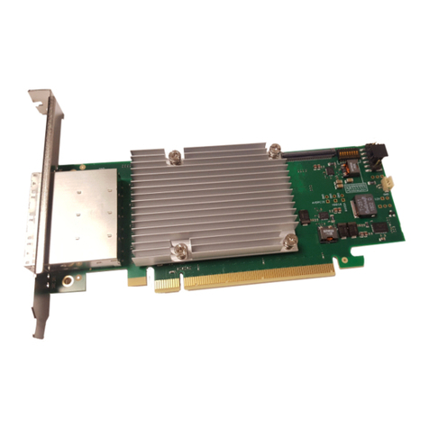
abaco systems PCI-5565PIORC Quick user guide

Hardware Reference Manual
PCI-5565PIORC* Ultrahigh Speed Fiber-
Optic Reflective Memory with Interrupts
THE PCI-5565PIORC IS DESIGNED TO MEET THE EUROPEAN UNION (EU)
RESTRICTIONS OF HAZARDOUS SUBSTANCE (RoHS) DIRECTIVE (2002/95/EC)
CURRENT REVISION.
Publication No. 500-9367855565-000 Rev. D.0

2 PCI-5565PIORC* Ultrahigh Speed Fiber-Optic Reflective Memory with Interrupts Publication No. 500-9367855565-000 Rev. D.0
Document History
Waste Electrical and Electronic Equipment (WEEE) Returns
Revision Date Description
C.0 March 2010 Hardware Reference Manual
D.0 October 2016 Reformatted
Abaco Systems is registered with an approved Producer Compliance Scheme (PCS) and, subject
to suitable contractual arrangements being in place, will ensure WEEE is processed in accordance
with the requirements of the WEEE Directive.
Abaco Systems will evaluate requests to take back products purchased by our customers before
August 13, 2005 on a case-by-case basis. A WEEE management fee may apply.

Publication No. 500-9367855565-000 Rev. D.0 About This Manual 3
About This Manual
Conventions
Notices
This manual may use the following types of notice:
WARNING
Warnings alert you to the risk of severe personal injury.
CAUTION
Cautions alert you to system danger or loss of data.
NOTE
Notes call attention to important features or instructions.
TIP
Tips give guidance on procedures that may be tackled in a number of ways.
LINK
Links take you to other documents or websites.
Numbers
All numbers are expressed in decimal, except addresses and memory or register
data, which are expressed in hexadecimal. Where confusion may occur, decimal
numbers have a “D” subscript and binary numbers have a “b” subscript. The
prefix “0x” shows a hexadecimal number, following the ‘C’ programming
language convention. Thus:
One dozen = 12D= 0x0C = 1100b
The multipliers “k”, “M” and “G” have their conventional scientific and
engineering meanings of x103, x106and x109respectively. The only exception to
this is in the description of the size of memory areas, when “k”, “M” and “G”
mean x210, x220 and x230 respectively.
NOTE
When describing transfer rates, “k”, “M” and “G” mean x103, x106and x109not x210, x220 and x230.
In PowerPC terminology, multiple bit fields are numbered from 0 to n where 0 is
the MSB and n is the LSB. PCI terminology follows the more familiar convention
that bit 0 is the LSB and n is the MSB.
Text
Signal names ending with a tilde (“~”) denote active low signals; all other signals
are active high. “N” and “P” denote the low and high components of a differential
signal respectively.

4 PCI-5565PIORC* Ultrahigh Speed Fiber-Optic Reflective Memory with Interrupts Publication No. 500-9367855565-000 Rev. D.0
Further Information
Abaco Website
You can find information regarding Abaco Systems products on the following
website:
LINK
www.abaco.com
Abaco Documents
This document is distributed via the Abaco website. You may register for access to
manuals via the website.
LINK
www.abaco.com/products/pci-5565piorc
Third-party Documents
Refer to PCI Local Bus Specification for a detailed explanation of the PCI Local bus from
the following source:
PCI Local Bus Specification, Rev. 2.2
PCI Special Interest Group
P.O. Box 14070
Portland, OR 97214
(800) 433-5177 (U.S.)
(503) 797-4207 (International)
(503) 234-6762 (FAX)
For information on PLD Applications’ PCI-X IP Core, contact them at:
United States
PLD Applications, Inc.
2570 North First St. 2nd floor
San Jose, CA 95131-1036
(408) 273 4530 or (866) 513 0362
Fax: (408) 273 4555
France (Corporate Headquarters)
PLD Applications
Europarc Pichaury A2 - 1330, rue Guillibert
13856 Aix-en-Provence Cedex 3 - France
Tel: +33 442 393 600
Fax: +33 442 394 902

Publication No. 500-9367855565-000 Rev. D.0 About This Manual 5
Technical Support Contact Information
You can find technical assistance contact details on the website Embedded
Support page.
LINK
www.abaco.com/embedded-support
Abaco will log your query in the Technical Support database and allocate it a
unique Case number for use in any future correspondence.
Alternatively, you may also contact Abaco’s Technical Support via:
LINK
Returns
If you need to return a product, there is a Return Materials Authorization (RMA)
form available via the website Embedded Support page.
LINK
www.abaco.com/embedded-support
Do not return products without first contacting the Abaco Repairs facility.
Additional Notes
The PCI-5565PIORC* is the PCI-based member of Abaco’s family of Reflective
Memory real-time fiber-optic network products. Two or more PCI-5565PIORCs,
along with other members of this family, can be integrated into a network using
standard fiber-optic cables. Each board in the network is referred to as a “node.”
Reflective Memory allows computers, workstations, PLCs and other embedded
controllers with different architectures and dissimilar operating systems to share
data in real-time. The 5565 family of Reflective Memory (referred to as RFM-5565
in this manual) is fast, flexible and easy to operate. Data is transferred by writing
to memory (SDRAM), which appears to reside globally in all boards on the
network. Onboard circuitry automatically performs the data transfer to all other
nodes with little or no involvement of any host processor. A block diagram of the
PCI-5565PIORC is shown in Figure 1.
Features
Features include:
• High speed, easy to use fiber-optic network (2.12 GBaud serially)
• 33MHz 64-bit/32-bit compatible PCI bus, 3.3 V or 5.0V logic level
• 66MHz 64-bit/32-bit compatible PCI bus, 3.3V logic level
• No host processor involvement in the operation of the network
• Selectable Redundant Mode of Operation

6 PCI-5565PIORC* Ultrahigh Speed Fiber-Optic Reflective Memory with Interrupts Publication No. 500-9367855565-000 Rev. D.0
• Up to 256 nodes
• Connectivity with multimode fiber up to 300 m, singlemode fiber up to
10 km
• Dynamic packet size, 4 to 64 bytes of data per packet
• Fiber network transfer rate 43 MByte/s to 170 MByte/s
• 128/256 MBytes SDRAM Reflective Memory with selectable parity
• Independent Direct Memory Access (DMA) channel
• Four general purpose network interrupts; each with 32 bits of data
• Configurable endian conversion for multiple CPU architectures on the same
network
• Selectable PCI PIO window size from 2 MBytes to 64 MBytes to full installed
memory size
• Operating System support: Windows®2000, Windows XP, Linux®and
VxWorks®
• RoHS Compliant
PCI Local Bus Compliance
The PCI-5565PIORC complies with requirements of the PCI Local Bus Specification,
version 2.2.
Vendor and Device Identification
The PCI Configuration register reserved for the vendor ID has the value of $114A,
which designates Abaco. The PCI Configuration register reserved for the device
ID has the value of $5565, which is Abaco’s board type.
Subsystem Vendor ID and Subsystem ID
The PCI Configuration register reserved for the subsystem vendor ID has the
value of $1556, which designates PLD applications. The PCI Configuration
register reserved for the subsystem ID has the value of $0080, which is the PLD
Applications PCI-X core identification number.
Comparison of the PCI-5565PIORC and the PCI-5565*
The classic PCI-5565* contains several components which have been combined
into a single FPGA (Field Programmable Gate Array) in the PCI-5565PIORC. The
components that were combined include a PCI interface device by PLX
Technologies, three separate smaller FPGAs, a transmit FIFO, and a receive FIFO.
The PCI-5565PIORC adds greater design flexibility and improved performance
over the classic PCI-5565 in at least three areas.
1. The PCI-5565PIORC’s DMA burst and PIO single read access rates have an
improvement over the classic PCI-5565.
2. The PCI-5565PIORC’s access bandwidth for the onboard SDRAM memory
has doubled, improving the overall throughput.
3. The PCI-5565PIORC is field upgradeable as new features are added.
The classic PCI-5565 contained a group of control registers within the PLX device
as well as a separate group of RFM specific control registers located in an FPGA.

Publication No. 500-9367855565-000 Rev. D.0 About This Manual 7
Because the two registers groups physically reside in separate devices, they are
accessed through different regions of memory. The PCI-5565PIORC, on the other
hand, contains both groups of registers within the same FPGA. The two groups
could have been combined. However to provide software continuity and
backward compatibility, the two register groups have been maintained separately
as in the classic VMIPCI-5565. Further, the individual bit functions within the
registers, where applicable, are still compatible.
The PCI-5565PIORC does not include a second DMA engine.

8 PCI-5565PIORC* Ultrahigh Speed Fiber-Optic Reflective Memory with Interrupts Publication No. 500-9367855565-000 Rev. D.0
Block Diagram
Figure 1 Block Diagram of PCI-5565PIORC
133 MHz
Memory
32-bit Data
SERDES
106.25 MHz16-bit
2.125 GHz
Optics
Fiber-Optic Network
4-bit Parity
PCI bus
Rx Tx
FIFO
FIFO
Main FPGA
PCI Core
32/64-bit at 33/66 MHz

Publication No. 500-9367855565-000 Rev. D.0 About This Manual 9
Figure 2Typical Reflective Memory Network
PCI WorkStation
with
PCI-5565PIORC
NODE 1
PCI-5565PIORC
VMEbus Chassis
with
PMC-5565PIORC
NODE 255
Up to 300m
between nodes
for multimode
VMEbus Chassis
with
VMIVME-5565
NODE 0
VMIVME
VMIVME
5565
5565
VMIVME
-5565
PMC-5565PIORC
Up to 10km
between nodes
for single mode

10 PCI-5565PIORC* Ultrahigh Speed Fiber-Optic Reflective Memory with Interrupts Publication No. 500-9367855565-000 Rev. D.0
Safety Summary
The following general safety precautions must be observed during all phases of
the operation, service and repair of this product. Failure to comply with these
precautions or with specific warnings elsewhere in this manual violates safety
standards of the design, manufacture, and intended use of this product.
Abaco assumes no liability for the customerʹs failure to comply with these
requirements.
Ground the System
To minimize shock hazard, the chassis and system cabinet must be connected to
an electrical ground. A three-conductor AC power cable should be used. The
power cable must either be plugged into an approved three-contact electrical
outlet or used with a three-contact to two-contact adapter with the grounding
wire (green) firmly connected to an electrical ground (safety ground) at the power
outlet.
Do Not Operate in an Explosive Atmosphere
Do not operate the system in the presence of flammable gases or fumes. Operation
of any electrical system in such an environment constitutes a definite safety
hazard.
Keep Away from Live Circuits
Operating personnel must not remove product covers. Component replacement
and internal adjustments must be made by qualified maintenance personnel. Do
not replace components with power cable connected. Under certain conditions,
dangerous voltages may exist even with the power cable removed. To avoid
injuries, always disconnect power and discharge circuits before touching them.
Do Not Service or Adjust Alone
Do not attempt internal service or adjustment unless another person capable of
rendering first aid and resuscitation is present.
Do Not Substitute Parts or Modify System
Because of the danger of introducing additional hazards, do not install substitute
parts or perform any unauthorized modification to the product. Return the
product to Abaco for service and repair to ensure that safety features are
maintained.

Publication No. 500-9367855565-000 Rev. D.0 About This Manual 11
Compliance Information
This chapter provides the applicable information regarding regulatory
compliance for the PCI-5565PIORC.
CE
Abaco has evaluated the PCI-5565PIORC has met the requirements for
compliance to the following standards:
• BS EN55024
• BS EN55022, Class A
• IEC61000-4-2
• IEC61000-4-3
International Compliance
It has also met the following international levels.
European Union
• BS EN55024 (1998 w A1:01 & A2: 03)
• CISPR22, EN55022 (Class A)
• CISPR11, EN55011(Class A, Group 1)
United States
• FCC Part 15, Subpart B, Section 109, Class A
• CISPR 22 (1997), Class A
• ANSI C63.4 (2003) method
Australia/New Zealand
• AS/NZS CISPR 22 (2002) Class A using:
• EN55022 (1998) Class A
Japan
• VCCI (April 2005) Class A using:
• CISPR 22 (1997) Class A
• ANSI C63.4 (2003) method
Canada
• ICES-003 Class A using:
• CISPR 22 (1997) Class A
• ANSI C63.4 (2003) Method

12 PCI-5565PIORC* Ultrahigh Speed Fiber-Optic Reflective Memory with Interrupts Publication No. 500-9367855565-000 Rev. D.0
FCC Part 15
This device complies with Part 15 of the FCC Rules. Operation is subject to the
following two conditions: (1) this device may not cause harmful interference, and
(2) this device must accept any interference received, including interference that
may cause undesired operation.
FCC Class A
NOTE
This equipment has been tested and found to comply with the limits for a Class A digital device,
pursuant to Part 15 of the FCC Rules. These limits are designed to provide reasonable protection against
harmful interference when the equipment is operated in a commercial environment. This equipment
generates, uses, and can radiate radio frequency energy and, if not installed and used in accordance with
the instruction manual, may cause harmful interference to radio communications. Operation of this
equipment in a residential area is likely to cause harmful interference in which case the user will be
required to correct the interference at his own expense.
CAUTION
Changes or modifications not expressly approved by the party responsible for compliance could void
the user’s authority to operate the equipment.
Canadian Regulations
The PCI-5565PIORC Class A digital apparatus complies with Canadian
ICES-003.
NOTE
Any equipment tested and found compliant with FCC Part 15 for unintentional radiators or EN55022
(previously CISPR 22) satisfy ICES-003.

Publication No. 500-9367855565-000 Rev. D.0 Table of Contents 13
Table of Contents
1 • Handling and Installation . . . . . . . . . . . . . . . . . . . . . . . . . . . . . . . . . . . . . . . . . . . . . . . . . . . . . 17
1.1 Unpacking Procedures. . . . . . . . . . . . . . . . . . . . . . . . . . . . . . . . . . . . . . . . . . . . . . . . . . . . . . . . . . . . . . . . . . . . 17
1.2 Handling Precaution. . . . . . . . . . . . . . . . . . . . . . . . . . . . . . . . . . . . . . . . . . . . . . . . . . . . . . . . . . . . . . . . . . . . . . 17
1.3 Switch S1 and S2 Configuration. . . . . . . . . . . . . . . . . . . . . . . . . . . . . . . . . . . . . . . . . . . . . . . . . . . . . . . . . . . . 18
1.3.1 Before Installation Switch S1 and S2 Configuration . . . . . . . . . . . . . . . . . . . . . . . . . . . . . . . . . . . . . . . . . . . . . . . . . 18
1.4 Physical Installation. . . . . . . . . . . . . . . . . . . . . . . . . . . . . . . . . . . . . . . . . . . . . . . . . . . . . . . . . . . . . . . . . . . . . . 21
1.5 Front Panel Description. . . . . . . . . . . . . . . . . . . . . . . . . . . . . . . . . . . . . . . . . . . . . . . . . . . . . . . . . . . . . . . . . . . 22
1.5.1 LED Description . . . . . . . . . . . . . . . . . . . . . . . . . . . . . . . . . . . . . . . . . . . . . . . . . . . . . . . . . . . . . . . . . . . . . . . . . . . . . . . 23
1.6 Cable Configuration. . . . . . . . . . . . . . . . . . . . . . . . . . . . . . . . . . . . . . . . . . . . . . . . . . . . . . . . . . . . . . . . . . . . . . . 23
1.6.1 Connector Specification (Singlemode and Multimode): . . . . . . . . . . . . . . . . . . . . . . . . . . . . . . . . . . . . . . . . . . . . . . 23
2 • Theory of Operation . . . . . . . . . . . . . . . . . . . . . . . . . . . . . . . . . . . . . . . . . . . . . . . . . . . . . . . . . . 25
2.1 Basic Operation. . . . . . . . . . . . . . . . . . . . . . . . . . . . . . . . . . . . . . . . . . . . . . . . . . . . . . . . . . . . . . . . . . . . . . . . . . 25
2.2 Front Bezel LED Indicators. . . . . . . . . . . . . . . . . . . . . . . . . . . . . . . . . . . . . . . . . . . . . . . . . . . . . . . . . . . . . . . . . 25
2.3 RFM-5565 Register Sets. . . . . . . . . . . . . . . . . . . . . . . . . . . . . . . . . . . . . . . . . . . . . . . . . . . . . . . . . . . . . . . . . . . 26
2.4 Reflective Memory RAM. . . . . . . . . . . . . . . . . . . . . . . . . . . . . . . . . . . . . . . . . . . . . . . . . . . . . . . . . . . . . . . . . . . 26
2.5 Interrupt Circuits. . . . . . . . . . . . . . . . . . . . . . . . . . . . . . . . . . . . . . . . . . . . . . . . . . . . . . . . . . . . . . . . . . . . . . . . . 27
2.6 Network Interrupts. . . . . . . . . . . . . . . . . . . . . . . . . . . . . . . . . . . . . . . . . . . . . . . . . . . . . . . . . . . . . . . . . . . . . . . . 29
2.7 Redundant Transfer Mode of Operation. . . . . . . . . . . . . . . . . . . . . . . . . . . . . . . . . . . . . . . . . . . . . . . . . . . . . . 29
2.8 Rogue Packet Removal Operation. . . . . . . . . . . . . . . . . . . . . . . . . . . . . . . . . . . . . . . . . . . . . . . . . . . . . . . . . . . 30
3 • Programming . . . . . . . . . . . . . . . . . . . . . . . . . . . . . . . . . . . . . . . . . . . . . . . . . . . . . . . . . . . . . . . 31
3.1 PCI Configuration Registers. . . . . . . . . . . . . . . . . . . . . . . . . . . . . . . . . . . . . . . . . . . . . . . . . . . . . . . . . . . . . . . . 32
3.2 Local Configuration Registers. . . . . . . . . . . . . . . . . . . . . . . . . . . . . . . . . . . . . . . . . . . . . . . . . . . . . . . . . . . . . . 41
3.3 RFM Control and Status Registers. . . . . . . . . . . . . . . . . . . . . . . . . . . . . . . . . . . . . . . . . . . . . . . . . . . . . . . . . . 48
3.3.1 Board Revision Register . . . . . . . . . . . . . . . . . . . . . . . . . . . . . . . . . . . . . . . . . . . . . . . . . . . . . . . . . . . . . . . . . . . . . . . . 49
3.3.2 Board ID Register . . . . . . . . . . . . . . . . . . . . . . . . . . . . . . . . . . . . . . . . . . . . . . . . . . . . . . . . . . . . . . . . . . . . . . . . . . . . . . 49
3.3.3 Board Revision Build Register . . . . . . . . . . . . . . . . . . . . . . . . . . . . . . . . . . . . . . . . . . . . . . . . . . . . . . . . . . . . . . . . . . . 49
3.3.4 Node ID Register . . . . . . . . . . . . . . . . . . . . . . . . . . . . . . . . . . . . . . . . . . . . . . . . . . . . . . . . . . . . . . . . . . . . . . . . . . . . . . 49
3.3.5 Local Control and Status Register 1 . . . . . . . . . . . . . . . . . . . . . . . . . . . . . . . . . . . . . . . . . . . . . . . . . . . . . . . . . . . . . . 49
3.3.6 Local Interrupt Control Registers . . . . . . . . . . . . . . . . . . . . . . . . . . . . . . . . . . . . . . . . . . . . . . . . . . . . . . . . . . . . . . . . . 53
3.3.7 Network Target Data Register . . . . . . . . . . . . . . . . . . . . . . . . . . . . . . . . . . . . . . . . . . . . . . . . . . . . . . . . . . . . . . . . . . . 56
3.3.8 Network Target Node Register . . . . . . . . . . . . . . . . . . . . . . . . . . . . . . . . . . . . . . . . . . . . . . . . . . . . . . . . . . . . . . . . . . . 56
3.3.9 Network Interrupt Command Register . . . . . . . . . . . . . . . . . . . . . . . . . . . . . . . . . . . . . . . . . . . . . . . . . . . . . . . . . . . . 56
3.3.10 Interrupt 1 Sender Data FIFO . . . . . . . . . . . . . . . . . . . . . . . . . . . . . . . . . . . . . . . . . . . . . . . . . . . . . . . . . . . . . . . . . . . 57
3.3.11 Interrupt 1 Sender ID FIFO . . . . . . . . . . . . . . . . . . . . . . . . . . . . . . . . . . . . . . . . . . . . . . . . . . . . . . . . . . . . . . . . . . . . . 57
3.3.12 Interrupt 2 Sender Data FIFO . . . . . . . . . . . . . . . . . . . . . . . . . . . . . . . . . . . . . . . . . . . . . . . . . . . . . . . . . . . . . . . . . . . 57
3.3.13 Interrupt 2 Sender ID FIFO . . . . . . . . . . . . . . . . . . . . . . . . . . . . . . . . . . . . . . . . . . . . . . . . . . . . . . . . . . . . . . . . . . . . . 58
3.3.14 Interrupt 3 Sender Data FIFO . . . . . . . . . . . . . . . . . . . . . . . . . . . . . . . . . . . . . . . . . . . . . . . . . . . . . . . . . . . . . . . . . . . 58
3.3.15 Interrupt 3 Sender ID FIFO . . . . . . . . . . . . . . . . . . . . . . . . . . . . . . . . . . . . . . . . . . . . . . . . . . . . . . . . . . . . . . . . . . . . . 58
3.3.16 Interrupt 4 Sender Data FIFO . . . . . . . . . . . . . . . . . . . . . . . . . . . . . . . . . . . . . . . . . . . . . . . . . . . . . . . . . . . . . . . . . . . 58
3.3.17 Interrupt 4 Sender ID FIFO . . . . . . . . . . . . . . . . . . . . . . . . . . . . . . . . . . . . . . . . . . . . . . . . . . . . . . . . . . . . . . . . . . . . . 58
3.4 Example of a Block DMA Operation for RFM-5565. . . . . . . . . . . . . . . . . . . . . . . . . . . . . . . . . . . . . . . . . . . . . 60
3.5 Example of a Scatter-Gather DMA Operation for RFM-5565. . . . . . . . . . . . . . . . . . . . . . . . . . . . . . . . . . . . . 61
3.6 Example of a PCI PIO Sliding Window Operation for RFM-5565. . . . . . . . . . . . . . . . . . . . . . . . . . . . . . . . . .63
3.7 Example of Network Interrupt Handling. . . . . . . . . . . . . . . . . . . . . . . . . . . . . . . . . . . . . . . . . . . . . . . . . . . . . . 65
3.7.1 Setup . . . . . . . . . . . . . . . . . . . . . . . . . . . . . . . . . . . . . . . . . . . . . . . . . . . . . . . . . . . . . . . . . . . . . . . . . . . . . . . . . . . . . . . . 65
3.7.2 Servicing Network Interrupts . . . . . . . . . . . . . . . . . . . . . . . . . . . . . . . . . . . . . . . . . . . . . . . . . . . . . . . . . . . . . . . . . . . . 65

14 PCI-5565PIORC* Ultrahigh Speed Fiber-Optic Reflective Memory with Interrupts Publication No. 500-9367855565-000 Rev. D.0
List of Figures
Figure 1 Block Diagram of PCI-5565PIORC. . . . . . . . . . . . . . . . . . . . . . . . . . . . . . . . . . . . . . . . . . . . . . . . . . . . . . . . . . . 8
Figure 2 Typical Reflective Memory Network . . . . . . . . . . . . . . . . . . . . . . . . . . . . . . . . . . . . . . . . . . . . . . . . . . . . . . . . . 9
Figure 1-1 S1 and S2 Location PCI-5565PIORC . . . . . . . . . . . . . . . . . . . . . . . . . . . . . . . . . . . . . . . . . . . . . . . . . . . . . . . 20
Figure 1-2 Installing the PCI-5565PIORC . . . . . . . . . . . . . . . . . . . . . . . . . . . . . . . . . . . . . . . . . . . . . . . . . . . . . . . . . . . . 21
Figure 1-3 Front Panel of PCI-5565PIORC . . . . . . . . . . . . . . . . . . . . . . . . . . . . . . . . . . . . . . . . . . . . . . . . . . . . . . . . . . . 22
Figure 1-4 LC Type Fiber-Optic Cable Connector . . . . . . . . . . . . . . . . . . . . . . . . . . . . . . . . . . . . . . . . . . . . . . . . . . . . . 24
Figure 1-5 Example: Six Node Ring Connectivity PCI-5565PIORC . . . . . . . . . . . . . . . . . . . . . . . . . . . . . . . . . . . . . . . 24
Figure 2-1 Interrupt Circuitry Block Diagram . . . . . . . . . . . . . . . . . . . . . . . . . . . . . . . . . . . . . . . . . . . . . . . . . . . . . . . . . 28
Figure 3-1 Block Diagram of the Network Interrupt Reception Circuitry . . . . . . . . . . . . . . . . . . . . . . . . . . . . . . . . . . 59

Publication No. 500-9367855565-000 Rev. D.0 List of Tables 15
List of Tables
Table 1-1 Example Node ID Switch S2 RFM-5565 . . . . . . . . . . . . . . . . . . . . . . . . . . . . . . . . . . . . . . . . . . . . . . . . . . . . . 19
Table 1-2 Switch S1 Configuration RFM-5565 . . . . . . . . . . . . . . . . . . . . . . . . . . . . . . . . . . . . . . . . . . . . . . . . . . . . . . . . 19
Table 1-3 S1 Memory Size . . . . . . . . . . . . . . . . . . . . . . . . . . . . . . . . . . . . . . . . . . . . . . . . . . . . . . . . . . . . . . . . . . . . . . . . 19
Table 1-4 LED Descriptions . . . . . . . . . . . . . . . . . . . . . . . . . . . . . . . . . . . . . . . . . . . . . . . . . . . . . . . . . . . . . . . . . . . . . . . 23
Table 1-5 Cable Specifications for Multimode and Singlemode . . . . . . . . . . . . . . . . . . . . . . . . . . . . . . . . . . . . . . . . . 23
Table 3-1 PCI Configuration Registers . . . . . . . . . . . . . . . . . . . . . . . . . . . . . . . . . . . . . . . . . . . . . . . . . . . . . . . . . . . . . . 32
Table 3-2 PCI Configuration ID Registers . . . . . . . . . . . . . . . . . . . . . . . . . . . . . . . . . . . . . . . . . . . . . . . . . . . . . . . . . . . . 32
Table 3-3 PCI Command Register . . . . . . . . . . . . . . . . . . . . . . . . . . . . . . . . . . . . . . . . . . . . . . . . . . . . . . . . . . . . . . . . . . 33
Table 3-4 PCI Status Register . . . . . . . . . . . . . . . . . . . . . . . . . . . . . . . . . . . . . . . . . . . . . . . . . . . . . . . . . . . . . . . . . . . . . 34
Table 3-5 PCI Revision ID Register . . . . . . . . . . . . . . . . . . . . . . . . . . . . . . . . . . . . . . . . . . . . . . . . . . . . . . . . . . . . . . . . . 35
Table 3-6 PCI Class Code Register . . . . . . . . . . . . . . . . . . . . . . . . . . . . . . . . . . . . . . . . . . . . . . . . . . . . . . . . . . . . . . . . . 35
Table 3-7 PCI Cache Line Size Register . . . . . . . . . . . . . . . . . . . . . . . . . . . . . . . . . . . . . . . . . . . . . . . . . . . . . . . . . . . . . 35
Table 3-8 PCI Latency Timer Register . . . . . . . . . . . . . . . . . . . . . . . . . . . . . . . . . . . . . . . . . . . . . . . . . . . . . . . . . . . . . . 35
Table 3-9 PCI Header Type Register . . . . . . . . . . . . . . . . . . . . . . . . . . . . . . . . . . . . . . . . . . . . . . . . . . . . . . . . . . . . . . . . 35
Table 3-10 PCI Built-in Self Test Register . . . . . . . . . . . . . . . . . . . . . . . . . . . . . . . . . . . . . . . . . . . . . . . . . . . . . . . . . . . 36
Table 3-11 PCI Base Address Register 0 for Access to Local Configuration Registers . . . . . . . . . . . . . . . . . . . . . . 36
Table 3-12 PCI Base Address Register 1 for Access to Local Configuration Registers . . . . . . . . . . . . . . . . . . . . . . 37
Table 3-13 PCI Base Address Register 2 for Access to RFM Control and Status Registers . . . . . . . . . . . . . . . . . . 37
Table 3-14 PCI Base Address Register 3 for Access to Reflective Memory . . . . . . . . . . . . . . . . . . . . . . . . . . . . . . . 38
Table 3-15 PCI Base Address Register 4 . . . . . . . . . . . . . . . . . . . . . . . . . . . . . . . . . . . . . . . . . . . . . . . . . . . . . . . . . . . . 38
Table 3-16 PCI Base Address Register 5 . . . . . . . . . . . . . . . . . . . . . . . . . . . . . . . . . . . . . . . . . . . . . . . . . . . . . . . . . . . . 39
Table 3-17 PCI Cardbus CIS Pointer Register . . . . . . . . . . . . . . . . . . . . . . . . . . . . . . . . . . . . . . . . . . . . . . . . . . . . . . . . 39
Table 3-18 PCI Subsystem Vendor ID Register . . . . . . . . . . . . . . . . . . . . . . . . . . . . . . . . . . . . . . . . . . . . . . . . . . . . . . . 39
Table 3-19 PCI Subsystem ID Register . . . . . . . . . . . . . . . . . . . . . . . . . . . . . . . . . . . . . . . . . . . . . . . . . . . . . . . . . . . . . . 39
Table 3-20 PCI Expansion ROM Base Register . . . . . . . . . . . . . . . . . . . . . . . . . . . . . . . . . . . . . . . . . . . . . . . . . . . . . . . 39
Table 3-21 PCI Capability Pointer Register . . . . . . . . . . . . . . . . . . . . . . . . . . . . . . . . . . . . . . . . . . . . . . . . . . . . . . . . . . 40
Table 3-22 PCI Interrupt Line . . . . . . . . . . . . . . . . . . . . . . . . . . . . . . . . . . . . . . . . . . . . . . . . . . . . . . . . . . . . . . . . . . . . . . 40
Table 3-23 PCI Interrupt Pin . . . . . . . . . . . . . . . . . . . . . . . . . . . . . . . . . . . . . . . . . . . . . . . . . . . . . . . . . . . . . . . . . . . . . . . 40
Table 3-24 PCI Min_Gnt . . . . . . . . . . . . . . . . . . . . . . . . . . . . . . . . . . . . . . . . . . . . . . . . . . . . . . . . . . . . . . . . . . . . . . . . . . 40
Table 3-25 PCI Max_Lat . . . . . . . . . . . . . . . . . . . . . . . . . . . . . . . . . . . . . . . . . . . . . . . . . . . . . . . . . . . . . . . . . . . . . . . . . . 40
Table 3-26 Local Configuration and DMA Control Registers . . . . . . . . . . . . . . . . . . . . . . . . . . . . . . . . . . . . . . . . . . . . 41
Table 3-27 Mode/DMA Arbitration Register . . . . . . . . . . . . . . . . . . . . . . . . . . . . . . . . . . . . . . . . . . . . . . . . . . . . . . . . . . 42
Table 3-28 Big/Little Endian Descriptor Register . . . . . . . . . . . . . . . . . . . . . . . . . . . . . . . . . . . . . . . . . . . . . . . . . . . . . 42
Table 3-29 Interrupt Control and Status Register . . . . . . . . . . . . . . . . . . . . . . . . . . . . . . . . . . . . . . . . . . . . . . . . . . . . . 43
Table 3-30 INTCSR Interrupt Enables . . . . . . . . . . . . . . . . . . . . . . . . . . . . . . . . . . . . . . . . . . . . . . . . . . . . . . . . . . . . . . . 43
Table 3-31 INTCSR Interrupt Status . . . . . . . . . . . . . . . . . . . . . . . . . . . . . . . . . . . . . . . . . . . . . . . . . . . . . . . . . . . . . . . . 44
Table 3-32 PCI Core/Features Revision ID . . . . . . . . . . . . . . . . . . . . . . . . . . . . . . . . . . . . . . . . . . . . . . . . . . . . . . . . . . . 44
Table 3-33 DMA Channel 0 Mode Register . . . . . . . . . . . . . . . . . . . . . . . . . . . . . . . . . . . . . . . . . . . . . . . . . . . . . . . . . . 44
Table 3-34 DMA Channel 0 PCI Address Register . . . . . . . . . . . . . . . . . . . . . . . . . . . . . . . . . . . . . . . . . . . . . . . . . . . . . 44
Table 3-35 DMA Channel 0 Local Address Register . . . . . . . . . . . . . . . . . . . . . . . . . . . . . . . . . . . . . . . . . . . . . . . . . . . 45
Table 3-36 DMA Channel 0 Transfer Size (Bytes) Register . . . . . . . . . . . . . . . . . . . . . . . . . . . . . . . . . . . . . . . . . . . . . 45
Table 3-37 DMA Channel 0 Descriptor Pointer Register . . . . . . . . . . . . . . . . . . . . . . . . . . . . . . . . . . . . . . . . . . . . . . . . 45
Table 3-38 DMA Channel 0 Command/Status Register . . . . . . . . . . . . . . . . . . . . . . . . . . . . . . . . . . . . . . . . . . . . . . . . 45
Table 3-39 DMA Channel 0 PCI Dual Address Cycles Upper Address . . . . . . . . . . . . . . . . . . . . . . . . . . . . . . . . . . . . . 46

16 PCI-5565PIORC* Ultrahigh Speed Fiber-Optic Reflective Memory with Interrupts Publication No. 500-9367855565-000 Rev. D.0
Table 3-40 PCI PIO Direct Slave Local Address Range . . . . . . . . . . . . . . . . . . . . . . . . . . . . . . . . . . . . . . . . . . . . . . . . . 46
Table 3-41 PCI PIO Direct Slave Local Base Address (Remap) . . . . . . . . . . . . . . . . . . . . . . . . . . . . . . . . . . . . . . . . . . 46
Table 3-42 Memory Map of the Local Control and Status Registers . . . . . . . . . . . . . . . . . . . . . . . . . . . . . . . . . . . . . 48
Table 3-43 Local Control and Status Register 1 . . . . . . . . . . . . . . . . . . . . . . . . . . . . . . . . . . . . . . . . . . . . . . . . . . . . . . 49
Table 3-44 PCI PIO Window Sizes . . . . . . . . . . . . . . . . . . . . . . . . . . . . . . . . . . . . . . . . . . . . . . . . . . . . . . . . . . . . . . . . . . 51
Table 3-45 Config 1 and Config 0 Memory Size . . . . . . . . . . . . . . . . . . . . . . . . . . . . . . . . . . . . . . . . . . . . . . . . . . . . . . 51
Table 3-46 Offset 1 and Offset 0 . . . . . . . . . . . . . . . . . . . . . . . . . . . . . . . . . . . . . . . . . . . . . . . . . . . . . . . . . . . . . . . . . . . 52
Table 3-47 Local Interrupt Status Register . . . . . . . . . . . . . . . . . . . . . . . . . . . . . . . . . . . . . . . . . . . . . . . . . . . . . . . . . . 53
Table 3-48 Local Interrupt Enable Register . . . . . . . . . . . . . . . . . . . . . . . . . . . . . . . . . . . . . . . . . . . . . . . . . . . . . . . . . . 56
Table 3-49 Network Interrupt Command Register . . . . . . . . . . . . . . . . . . . . . . . . . . . . . . . . . . . . . . . . . . . . . . . . . . . . . 57
Table 3-50 DMA Registers . . . . . . . . . . . . . . . . . . . . . . . . . . . . . . . . . . . . . . . . . . . . . . . . . . . . . . . . . . . . . . . . . . . . . . . . 60
Table 3-51 DMA Channel 0 Mode Settings . . . . . . . . . . . . . . . . . . . . . . . . . . . . . . . . . . . . . . . . . . . . . . . . . . . . . . . . . . 62
Table 3-52 PCI PIO Window Selections . . . . . . . . . . . . . . . . . . . . . . . . . . . . . . . . . . . . . . . . . . . . . . . . . . . . . . . . . . . . . 63

Publication No. 500-9367855565-000 Rev. D.0 Handling and Installation 17
1 • Handling and Installation
This chapter describes the installation and configuration of the board. Cable
configuration and board layout are illustrated in this chapter.
1.1 Unpacking Procedures
Any precautions found in the shipping container should be observed. All items
should be carefully unpacked and thoroughly inspected for damage that might
have occurred during shipment. The board(s) should be checked for broken
components, damaged printed circuit board(s), heat damage and other visible
contamination. All claims arising from shipping damage should be filed with the
carrier and a complete report sent to Abaco Systems Customer Care.
1.2 Handling Precaution
Some of the components assembled on Abaco’s products may be sensitive to
electrostatic discharge and damage may occur on boards that are subjected to a
high-energy electrostatic field. When the board is placed on a bench for
configuring, etc., it is suggested that conductive material should be placed under
the board to provide a conductive shunt. Unused boards should be stored in the
same protective boxes in which they were shipped.

18 PCI-5565PIORC* Ultrahigh Speed Fiber-Optic Reflective Memory with Interrupts Publication No. 500-9367855565-000 Rev. D.0
1.3 Switch S1 and S2 Configuration
Prior to installing the RFM-5565 in a host system, the desired node ID must be set
using switch S2. Each node in the network must have a unique node ID. See
Figure 1-1 for the location of switch S2.
Switch S2 corresponds to 8 node ID select signal lines. The 8 node ID select lines
permit any binary node ID from 0 to $FF (255 decimal). Switch S2 position 1
corresponds to the least significant node ID line and switch S2 position 8
corresponds to the most significant node ID line. Placing switch S2 in the OFF
position sets the binary node ID line low (0), while placing switch S2 in the ON
position sets the binary node ID line high (1). Table 1-1 provides examples of
possible node IDs.
1.3.1 Before Installation Switch S1 and S2 Configuration
NOTE
ALL nodes on the ring MUST be configured for the SAME transfer mode: either redundant or non-
redundant transfer mode. A mismatch of this setting will result in certain packets being removed from
the ring, and that data will be lost.
NOTE
No more than one node on the ring should be configured with Rogue Master 0 enabled. Certain packets
will be removed from the ring when two or more nodes are configured with Rogue
Master 0 enabled, and that data will be lost.
NOTE
No more than one node on the ring should be configured with Rogue Master 1 enabled. Certain packets
will be removed from the ring when two or more nodes are configured with Rogue
Master 1 enabled, and that data will be lost.
Prior to installing the RFM-5565 in the host system, switch S1 must be configured
for the appropriate mode of operation. Switch S1 controls six functions on the
board. Settings on Switch S1 should only be changed while power is off.
1. S1 position 1 selects the non-redundant (OFF position) or redundant
network transfer modes.
2. S1 position 2 selects between the low network usage (ON position) of the
classic 5565 boards or the higher performance achievable on this board (OFF
position).
3. S1 positions 3 and 4 select the PCI window size for PIO memory accesses.
The default (when both switch positions 3 and 4 are OFF) is to use the full
installed memory size. The reduced memory window size choices are
64 MBytes, 16 MBytes or 2 MBytes.
4. S1 position 5 enables (ON position) or disables the Rogue Master 0 function.
5. S1 position 6 enables (ON position) or disables the Rogue Master 1 function.
6. S1 position 8 selects between the factory default control logic (ON position)
or the most recent control logic flashed to the board (OFF position).
S1 position 7 is currently reserved and should not be used (left in the OFF
position).

Publication No. 500-9367855565-000 Rev. D.0 Handling and Installation 19
NOTE
S1 position 8 should be set in the ON position only when a flash update of the control logic has failed.
After a successful flash update of the control logic, S1 position 8 should be set in the OFF position.
Table 1-1 Example Node ID Switch S2 RFM-5565
S2
Position
8
S2
Position
7
S2
Position
6
S2
Position
5
S2
Position
4
S2
Position
3
S2
Position
2
S2
Position
1
Node ID
Hex
(Dec.)
ON ON ON ON ON ON ON ON $FF
(255)
ON OFF OFF OFF OFF OFF OFF OFF $80
(128)
OFF ON OFF OFF OFF OFF OFF OFF $40 (64)
OFF OFF ON OFF OFF OFF OFF OFF $20 (32)
OFFOFFOFFON OFFOFFOFFOFF$10(16)
OFF OFF OFF OFF ON OFF OFF OFF $8 (8)
OFFOFFOFFOFFOFFON OFFOFF$4(4)
OFF OFF OFF OFF OFF OFF ON OFF $2 (2)
OFF OFF OFF OFF OFF OFF OFF ON $1 (1)
OFF OFF OFF OFF OFF OFF OFF OFF $0 (0)
Factory Default: S2 positions 1 through 8 OFF
Table 1-2 Switch S1 Configuration RFM-5565
Position 1 OFF (non-redundant mode)
Position 1 ON (redundant mode)
Position 2 OFF (higher performance achievable)
Position 2 ON (low network usage)
Position 5 OFF (disables Rogue Master 0)
Position 5 ON (enables Rogue Master 0)
Position 6 OFF (disables Rogue Master 1)
Position 6 ON (enables Rogue Master 1)
Position 8 OFF (most recent control logic)
Position 8 ON (original factory control logic)
Factory Defaults
Positions 1-8 OFF
Table 1-3 S1 Memory Size
PCI Window Size S1 Position 3 S1 Position 4
Default Off Off
64 MBytes On Off
16 MBytes Off On
2 MBytes On On

20 PCI-5565PIORC* Ultrahigh Speed Fiber-Optic Reflective Memory with Interrupts Publication No. 500-9367855565-000 Rev. D.0
Figure 1-1 S1 and S2 Location PCI-5565PIORC
Table of contents
Popular PCI Card manuals by other brands

SIIG
SIIG SC2475 Quick installation guide

TRENDnet
TRENDnet TEW-703PI Quick installation guide

ADLINK Technology
ADLINK Technology cPCI-3548 user manual

ICM Controls
ICM Controls ICM2915 Installation, operation & application guide

Advantech
Advantech PCI-1625U user manual

Delta Electronics
Delta Electronics PCI-DMC-A01 Programming user manual