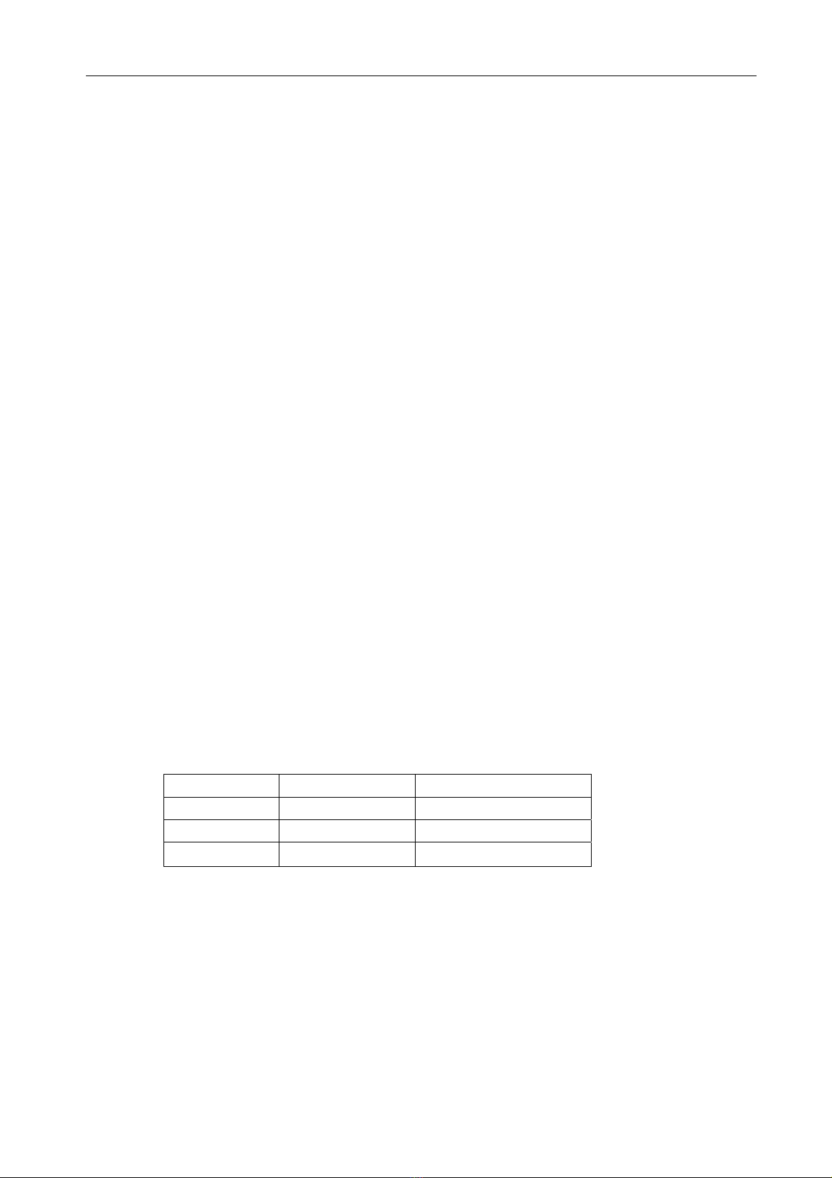
A-80 VHF SERVICE MANUAL
--9--
The first IF signal is amplified by Q302, and then enters IC300 (FM processing IC). The
signal is heterodyned again with a second local oscillator signal within IC300 to create a
455 KHz second IF signal. The second IF signal is then fed through a 455 KHz ceramic
filter (CF300) to further eliminate unwanted signals before it is amplified and FM detected
in IC300.
4)AF amplifier
The recovered AF signal obtained from IC300 is amplified by IC500D, filtered by the
high-pass filter IC500A to eliminate signals under 300Hz. And de-emphasized by R518
and C510. The processed AF signal passes through anAF volume control and is amplified
to a sufficient level to drive a loud speaker by anAF power amplifier (IC2).
5)Squelch
Part of the AF signal from IC300 enters IC300 again, and the noise component is
amplified and rectified by a filter and an amplifier to produce a DC voltage corresponding
to the noise level.
The DC signal from the FM IC goes to the analog port of the microprocessor(IC1).IC1
determines whether to output sounds from the speaker by checking whether the input
voltage is higher or lower than the preset value.
To output sounds from the speaker, IC1 sends a high signal to the AFCO lines and turns
IC2 on through Q501, Q5, Q4, Q7 and Q6.
6)Receive signaling
QT/DQT
300Hz and higher audio frequencies of the output signal from IF IC are cut by a
low-pass filter (IC500 B/C). The resulting signal enters the microprocessor (IC1). IC1
determines whether the QT or DQT matches the preset value, and controls the MUTE and
AFCO and the speaker output sounds according to the squelch results.
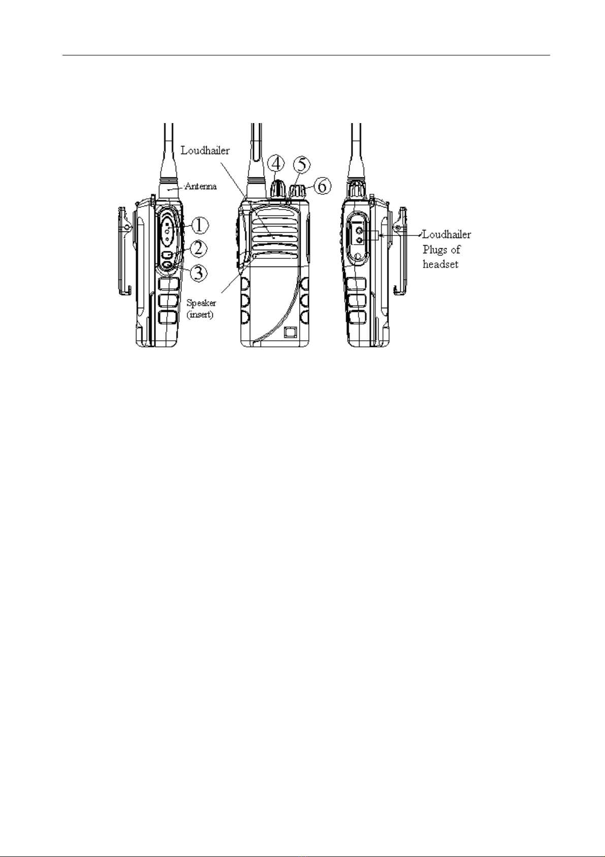
3. PLL frequency synthesizer
The PLL circuit generates the first local oscillator signal for reception and the RF signal
for transmission.
1)PLL
The frequency step of the PLL circuit is 2.5 or 3.125 kHz. A 12.8 MHz reference
oscillator signal is divided at IC6 by a fixed counter to produce the 2.5 or 3.125 kHz
reference frequency. The voltage controlled oscillator (VCO) output signal is buffer
amplified by Q102, then divided in IC6 by a dual-module programmable counter. The
divided signal is compared in phase with the 2.5 or 3.125 kHz reference signal in the
phase comparator in IC6. The output signal from the phase comparator is filtered through
a low-pass filter and passed to the varactor diodes D102, D103 (RX), D100 and D101 (TX)