Active-semi ACT88325EVK1-101 User manual

UG125
Rev 1.0, 20-Jun-2018
Innovative Power
TM
ActiveSwitcher
TM
is a trademark of Active-Semi.
1
ACT88325EVK1-101 User’s Guide
Description
This document describes the characteristic and operation of the Active Semi ACT88325EVK1-101 evaluation
kit (EVK).It provides setup and operation instructions, schematic, layout, BOM, and test data. This EVK
demonstrates the ACT88325VA101ActivePMU power management IC. Other ACT88325VAxxx options can be
evaluated on this EVK by replacing the IC and any other necessary components.
Features
The EVK can be used as a standalone board if desired. However, to access the internal registers and to take
full advantage of the IC’s capability, the user must connect the EVK kit to a PC with Active Semi’s USB-TO-I2C
interface dongle and use the GUI software. The EVK provides full access to the each converter’s input and
output voltage, as well as all the digital control signals. This gives the user the flexibility to configure the EVK
to match their real world system.
Note that the ACT88325EVK1-101 is specifically configured for the ACT88325VA101. This CMI option is
configured to power the Silicon Motion 2263 and SM2263XT processors with a 3.3V input.
Figure 1 – EVK Picture
UG125
Rev 1.0, 20-Jun-2018
Innovative Power
TM
ActiveSwitcher
TM
is a trademark of Active-Semi.
2
EVK Contents
The ACT88325EVK1-101 evaluation kit comes with the following items?
1. EVK Assembly
2. USB-TO-I2C dongle
a. Dongle
b. Custom 4-pin connector that connects the USB-TO-I2C dongle to the EVK assembly.
Required Equipment
ACT88325EVK1-101
USB-TO-I2C Dongle
Power supply – 3.5V @ 4A for full power operation
Oscilloscope – >100MHz, >2 channels
Loads – Electronic or resistive. 3A minimum current capability.
Digital Multi-meters (DMM)
Windows compatible computer with spare USB port.
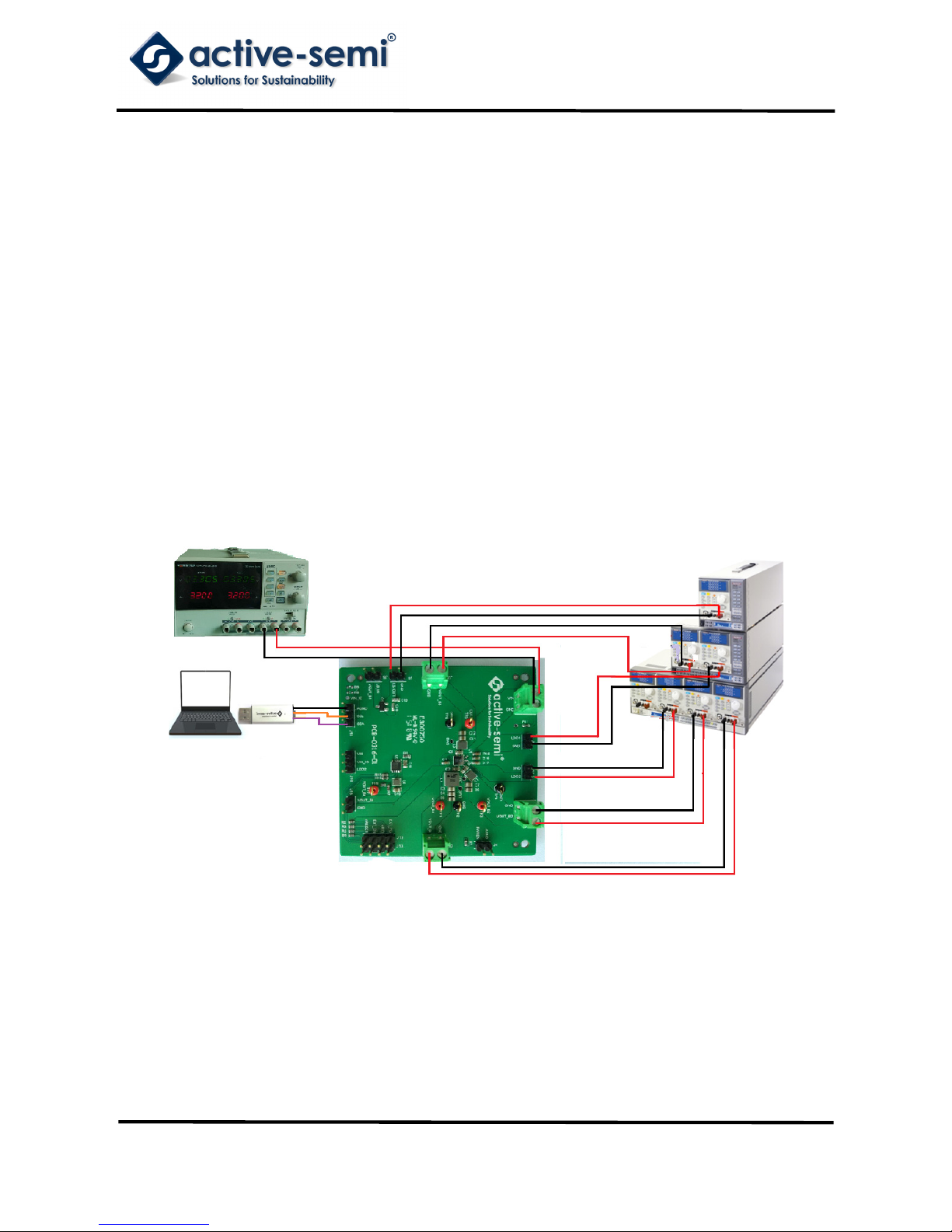
Hardware Setup
Figure 2 – EVK Setup

UG125
Rev 1.0, 20-Jun-2018
Innovative Power
TM
ActiveSwitcher
TM
is a trademark of Active-Semi.
3
Quick Start
Hardware Connections
Refer to Figure 2 for hardware connections.
1. Decide which voltage will power VIN_IO. Active Semi recommends powering VIN_IO from the VIN input
voltage. Connect a shorting jumper between J10-2 and J10-3 header to power VIN_IO from the VIN
input voltage.
Figure 3 – Shorting Jumper Settings
2. Connect a lab supply betweenJ1-1 and J1-2 to power VIN for the buck power supplies. Note that this is
the same input voltage to the LDOs. Separating the buck and LDO input voltage sources requires
careful consideration of startup sequencing.
3. Be careful to keep the input voltage within the specifications.
4. Connect an appropriate load to each power supply output.
5. Optional - Connect the EVK to the PC with the USB dongle.
6. Connect Digital Multi-Meters to the voltages of interest.
7. Apply 3.3V input power.
GUI Setup (optional)
1. Refer to the end of this document for detailed instructions to install the ACT88325 GUI.
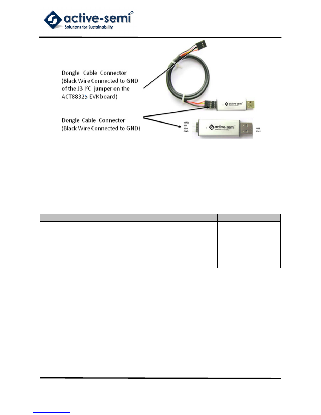
2. Connect the USB-TO-I2C dongle to the computer.
3. Connect the USB-TO-I2C dongle to the EVK J14 connector. Refer to Figure 4 to ensure the correct
polarity of the connection. As a guide, use the “Active-Semi” logo on the top of the dongle so the black
wire is connected to the Dongle GND pin.
UG125
Rev 1.0, 20-Jun-2018
Innovative Power
TM
ActiveSwitcher
TM
is a trademark of Active-Semi.
4
Figure 4 – USB-TO-I2C Dongle Connection
Recommended Operating Conditions
The ACT88325EVK1-101 is designed for a 3.3V input voltage. The maximum operating voltage is determined
by the IC’s maximum input voltage rating. The minimum operating voltages are determined by the buck
converters’ minimum input voltage and by the LDOs’ dropout voltages. Maximum currents are determined by
the IC’s CMI settings, which can be changed via I
2
C after startup.
Table1. Recommended Operating Conditions
Parameter Description Min Typ Max Unit
VIN All buck input voltages 2.7 5.5 V
I
B1_max
Maximum Buck 1 load current 4.0 A
I
B2_max
Maximum Buck 2 load current 3.0 A
I
B3_max
Maximum Buck 3 load current 2.0 A
I
LDO1_max
Maximum LDO 1 load current 0.3 A
I
LDO2_max
Maximum LDO 2 load current 0.3 A
Hardware Configuration
Input Voltage: Note that the ACT88325EVK1-101 uses the ACT88325VA101 IC. This IC can accept up to a
5.5V input voltage. However, the ACT88325VA101 IC is designed for a 3.3V input and shuts off if VIN goes
higher than 3.7V. Use the GUI to increase the SYSMON voltage to evaluate input voltages higher than 3.7V.
BUCK1: The ACT88325 BUCK1 output can be operated as a buck converter or in bypass mode. The CMI 101
is configured for bypass mode and passes the input voltage straight through to the output. Even though
BUCK1 is in bypass mode, the EVK still populates the BUCK1 inductor, L1, so other CMI options can be eas-
ily evaluated on the PCB.
ACT8310 External Supply:The EVK includes an external power supply, ACT8310, to demonstrate the ICs
sequencing capability. The ACT88325 EXT_EN output enables the ACT8310 at the proper time in the turn-on
sequencing. This external supply can be used to evaluate the flexible sequencing options in other CMI op-
tions.
DPSLP Function: The PWREN pinis configured to put the IC into DPSLP Mode to provide the SM2263 pro-
UG125
Rev 1.0, 20-Jun-2018
Innovative Power
TM
ActiveSwitcher
TM
is a trademark of Active-Semi.
5
cessor the PS4 power mode. Pull PWREN to ground by placing a shorting jumper on J4 to enter DPSLP-
mode. This turns off outputs BUCK1, BUCK3, and EXT_EN.
BUCK3 Output Voltage Select: Select BUCK3=1.2V by leaving nIRQ, GPIO3, high. Select BUCK3=1.8V by
shorting nIRQ to ground.
DVS: BUCK2 is 0.9V in normal operation and 0.75V in DVS mode. Pull EXT_PG, GPIO4 to ground to enable
DVS mode.
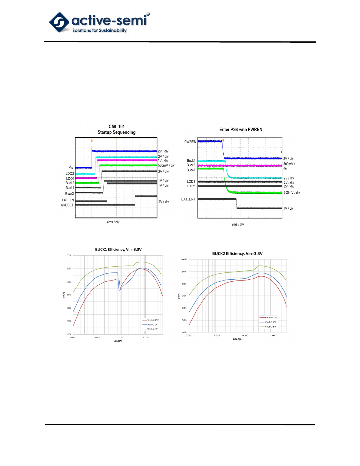
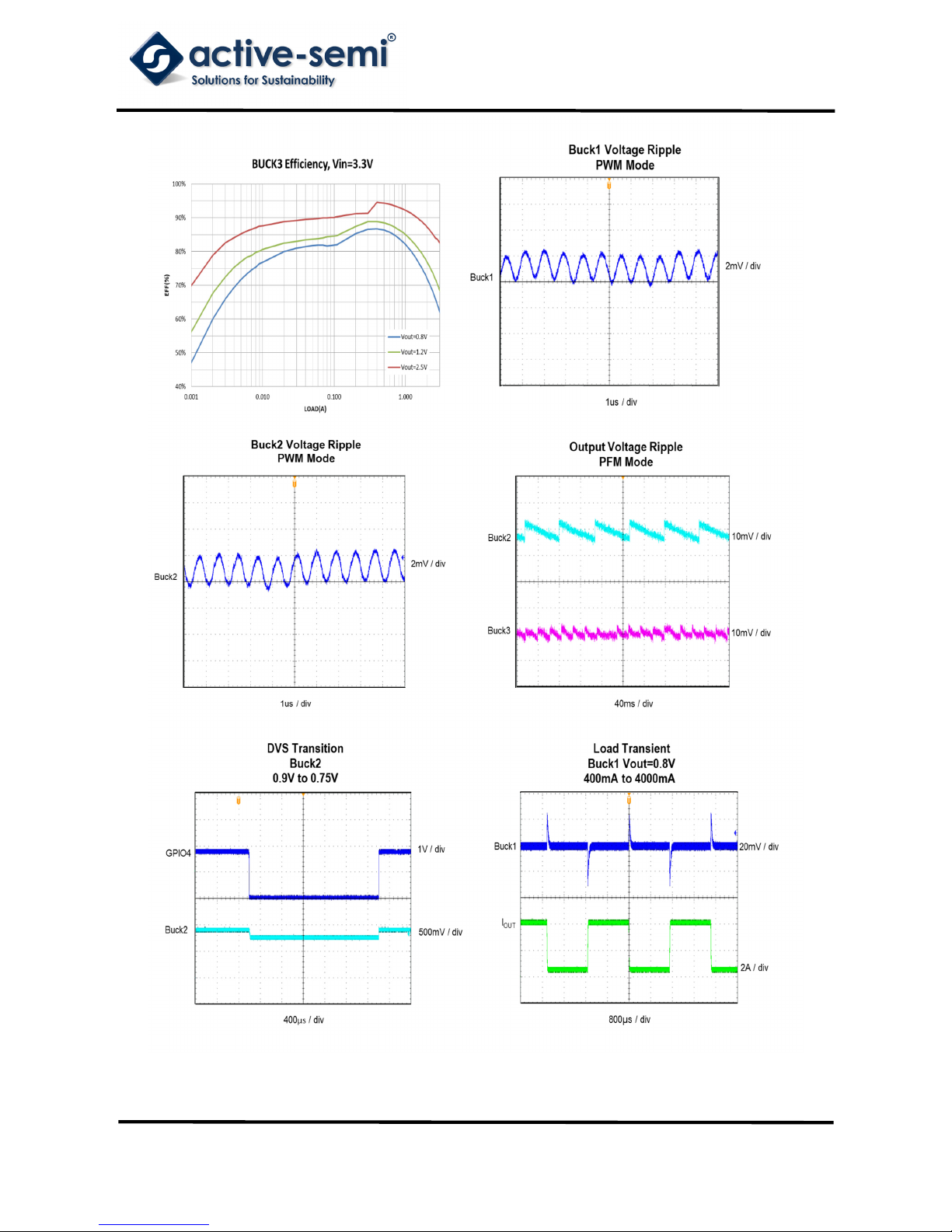
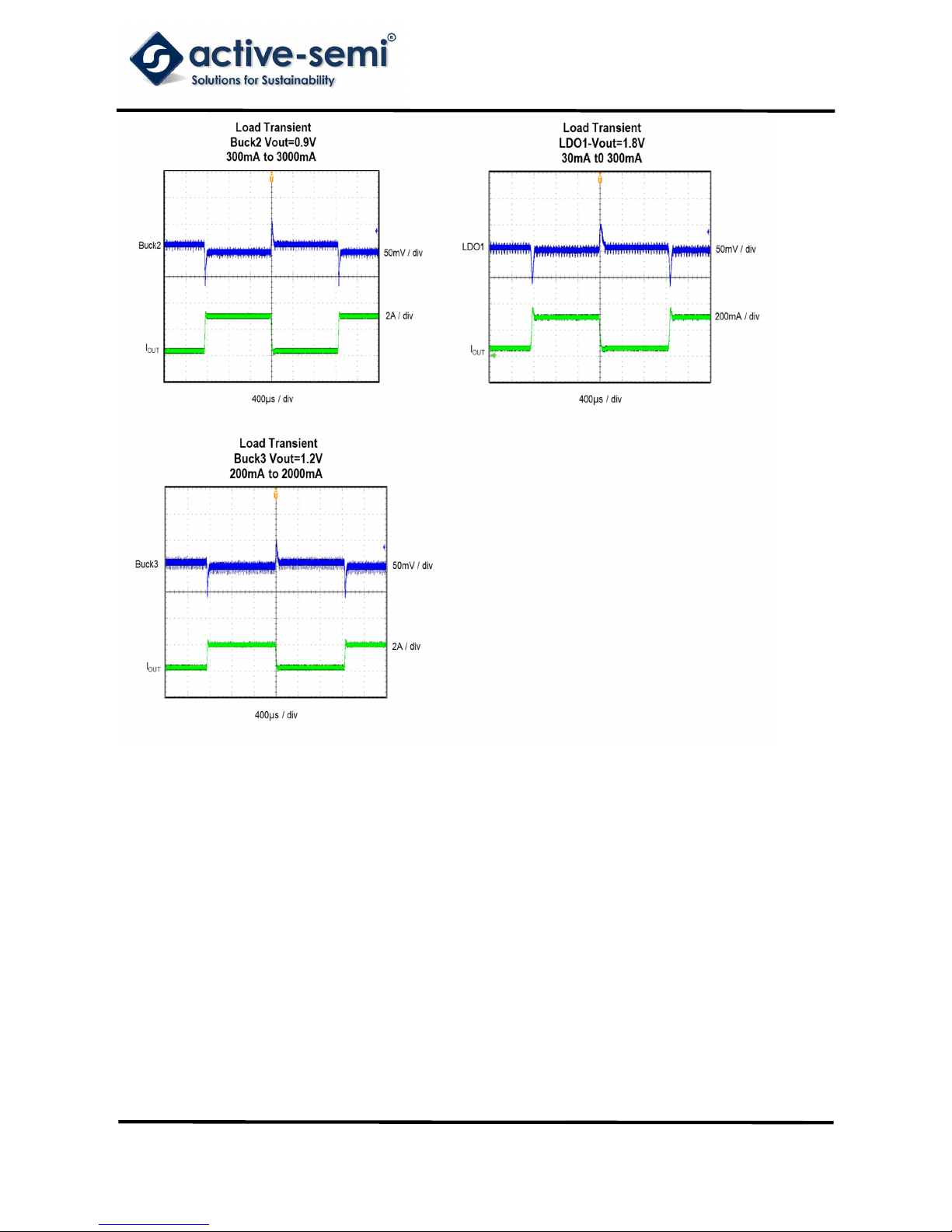
Test Results
UG125
Rev 1.0, 20-Jun-2018
Innovative Power
TM
ActiveSwitcher
TM
is a trademark of Active-Semi.
6
UG125
Rev 1.0, 20-Jun-2018
Innovative Power
TM
ActiveSwitcher
TM
is a trademark of Active-Semi.
7

UG125
Rev 1.0, 20-Jun-2018
Innovative Power
TM
ActiveSwitcher
TM
is a trademark of Active-Semi.
8
Schematic
Figure 5 – ACT88325EVK1-101 Schematic
VIN
SDA
SCL
DNP
R8
1
2
3
J14
2.54
VIN_IO
AGND
PWREN
VIN
VIN
LDO1
LDO2
S D
G
Q1
GND
GND
1
2
J6
2.54
GND
1nF
C13
1nF
C10
100k
R4
100k
R3
100k
R5
GND
100k
R2
VIN_IO
LDO2
FB_B3 A1
LDO1 B1
AV I N
C1
LDO2 D1
PWREN
E1
FB_B2 F1
VIN_B3 A2
VIN_B3 B2
LSG
C2
VIN_B2 D2
VIN_B2 E2
VIN_B2 F2
SW_B3 A3
SW_B3 A4
SW_B2 D3
SW_B2 E3
SW_B2 F3
PGND D4
PGND E4
PGND F4
PGND A5
SW_B1 D5
SW_B1 E5
SW_B1 F5
AGND A6
GPIO3
B6
GPIO2
C6
VIN_B1 D6
VIN_B1 E6
VIN_B1 F6
SDA
A7
SCL
B7
GPIO1
C7
GPIO4
D7
VIN_IO
E7
FB_B1 F7
U1
ACT88325
SCL
SDA
PWREN
VIN_IO
nRESET
nIRQ
EXT_EN
EXT_PG
LSG
AV I N
AGND
GND
GND
VIN
VIN
VIN
GND
GND
GND
1
2
J2
3.5mm
1uF
C17
1uF
C16
1uF
C1
SW1
SW2
SW3
TP1
TP3
TP5
SW2
SW3
nRESET
nIRQ
EXT_EN
EXT_PG
GND
GND
TP2
TP6
1
2
J5
3.5mm
1
2
J7
3.5mm
1
2
J1
3.5mm
DNP
R9
GND
GND
GND
GND
GND
GND
TP4
FID1
MAN,Fiducial
FID2
MAN,Fiducial
FID3
MAN,Fiducial
1
2
3
J10
2.54
1
2
J4
2.54
AGND
100k
R1
1
2
J9
2.54
1
2
J11
2.54
10uF
C18
22uF
C19
GND
0Ohm
R6
VIN
174k
R7
200k
R14
AGND
1
2
J8
2.54
TP7
1
2
J15
2.54
AGND VOUT B1
VOUT B2
VOUT B3
LDO1
LDO2
GND
GND
GND
GND
GND
GND
VIN
LS IN
VOUT B1
LS OUT
GND
VOUT B4
GND
SW1 VOUT_B1
VOUT_B2
VOUT_B3
VOUT_B1
IN
1
GP
2
IN
3
GND
4
FB 5
POK
6
EN
7
SW 8
EP
9
U2 ACT8311
GND
0Ohm
R10
0Ohm
R15
EXT_EN
EXT_PG
GND
1uHL3
1uHL2
1uHL1
1uHL4
22uF
C3
22uF
C4
22uF
C5
2.2uF
C15
10uF
C6
10uF
C2
0Ohm
R11
VIN
22uF
C7
22uF
C8
10uF
C9
22uF
C11
22uF
C12
1
2
3
4
J12
2.54
1
2
3
4
J13
2.54
Active-Semi
UG125
Rev 1.0, 20-Jun-2018
Innovative Power
TM
ActiveSwitcher
TM
is a trademark of Active-Semi.
9
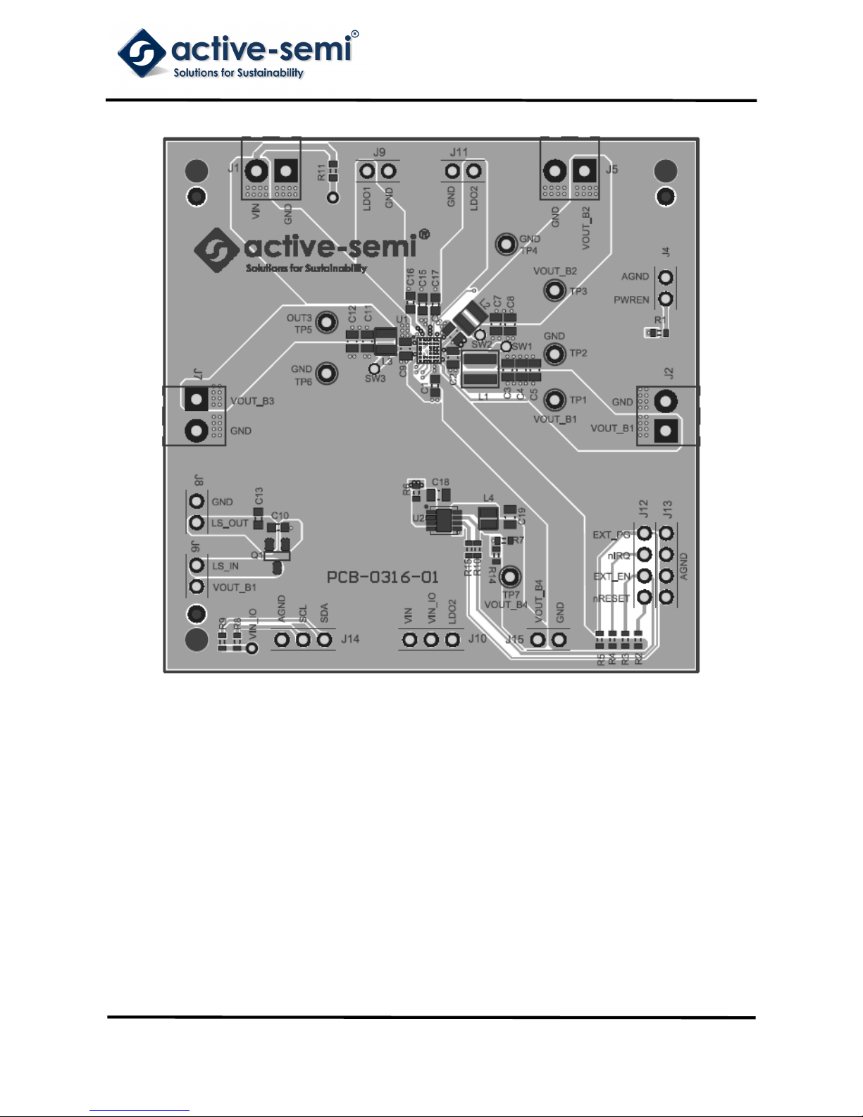
Layout
Figure 6 – Layout Top Assembly
UG125
Rev 1.0, 20-Jun-2018
Innovative Power
TM
ActiveSwitcher
TM
is a trademark of Active-Semi.
10
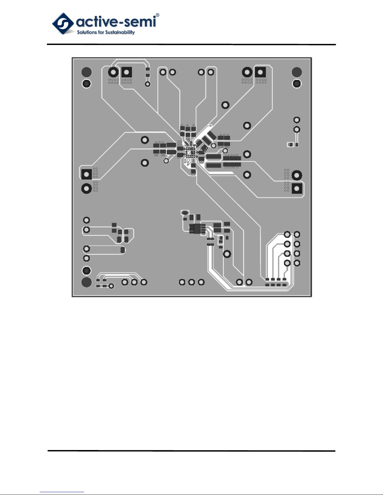
Figure 7 – Layout Top Layer
UG125
Rev 1.0, 20-Jun-2018
Innovative Power
TM
ActiveSwitcher
TM
is a trademark of Active-Semi.
11
Figure 8 – Layout Layer 2

UG125
Rev 1.0, 20-Jun-2018
Innovative Power
TM
ActiveSwitcher
TM
is a trademark of Active-Semi.
12
Figure 9 – Layout Layer 3

UG125
Rev 1.0, 20-Jun-2018
Innovative Power
TM
ActiveSwitcher
TM
is a trademark of Active-Semi.
13
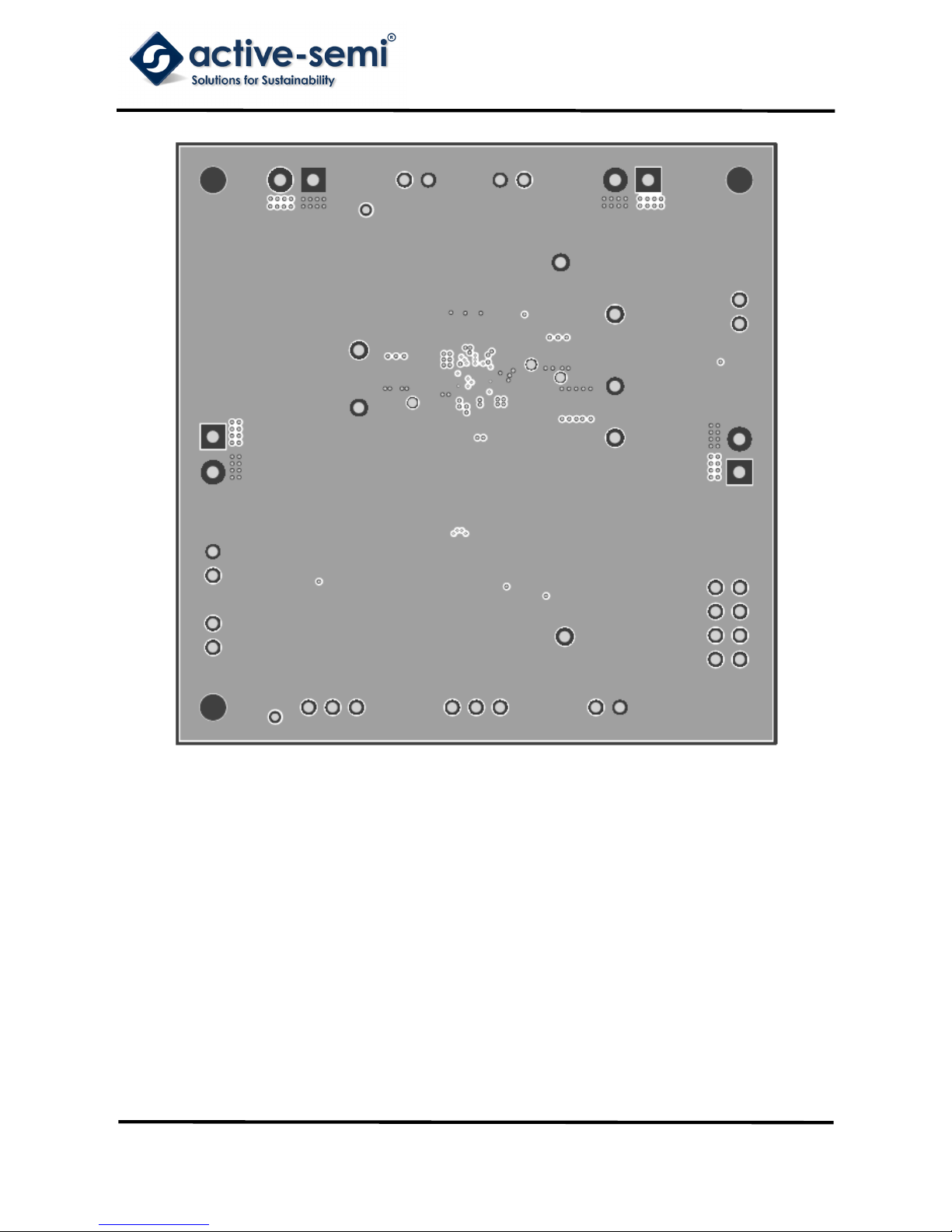
Figure 10 – Layout Bottom Layer

UG125
Rev 1.0, 20-Jun-2018
Innovative Power
TM
ActiveSwitcher
TM
is a trademark of Active-Semi.
14
Bill of Materials
Table 2 - BOM
Item Ref Des QTY Description Package MFR Part Number
1 C1 1 Cap, Ceramic, 1uF, 6.3V, 20%, X5R 0603 Yageo std
2 C2, C6, C9, C18 3 Cap, Ceramic, 10uF, 6.3V, 10%, X7R 0805 Yageo std
3 C3, C4, C5, C7, C8,
C11, C12, C19 8 Cap, Ceramic, 22uF, 10V, 100%, X7R 0805 Yageo std
4 C10, C13 2 Cap, Ceramic,1nF, 10V, 10%, X5R 0603 Yageo std
5 C15 1 Cap, Ceramic, 2.2uF, 10V, 10%, X5R 0603 Yageo std
6 C16, C17 2 Cap, Ceramic, 1uF, 10V, 20%, X5R 0603 Yageo std
7 C24 1 Cap, Ceramic,10uF, 10V, 20%, X5R 0805 Yageo std
8 J1, J2, J5, J7 4 Entry modular, 2 Pins, 3. 5mm Wurth Elektronik 691214110002
9 J4, J6, J8, J9, J11,
J15 6 Header, 2 pin CON2 Wurth Elektronik 61300211121
10 J10, J14 2 Header, 3 pin CON3 Wurth Elektronik 61300311121
11 J12, J13 2 Header, 4 pin CON4 Wurth Elektronik 61300411121
12 L1 1 Inductor, 1uH, 7.2A, 12mohm Wurth 4020 Wurth Elektronik 74438356010
13 L2, L3, L4 3 Inductor, 1uH, 2.5A, 63mohm Wurth 2510 Wurth Elektronik 74438323010
14 Q1 2 N-MOSFET, 30V/5.7A SOT23 AOS AO3404A
15 R1, R2, R3, R4, R5 5 Res, 100k, 1% 0603 Yageo std
16 R6, R10, R11, R15 4 Res, 0Ω, 1% 0603 Yageo std
17 R7 1 Res, 174kΩ, 1% 0603 Yageo std
18 R8, R9 0 Res, 10kΩ, 1% 0603 Yageo std
19 R13 1 Res, 174kΩ, 1% 0603 Yageo std
20 R14 1 Res, 200kΩ, 1% 0603 Yageo std
21 TP1, TP3, TP5, TP7 4 Test Point, Red 0.063" Keystone 5000
22 TP2, TP4, TP6 3 Test Point, Black 0.063" Keystone 5001
23 U1 1 IC, ACT88325 SCP-36 Active-semi ACT88325VA101-T
24 U2 1 IC, ACT8311, Buck converter TDFN33-8 Active-semi ACT8311NHADJ-T

UG125
Rev 1.0, 20-Jun-2018
Innovative Power
TM
ActiveSwitcher
TM
is a trademark of Active-Semi.
15
GUI Installation
1. Get GUI files from the Active Semi website
2. Plug the USB-TO-I2C dongle into a free USB port.
3. Follow the instructions in the “How to install driver for dongle” folder.
4. Double click on the ACT88325 GUI.exe to start the ACT88325 GUI.
Figure 11 – Dongle Driver
GUI Overview
The GUI has 2 basic function buttons allocated in top-left of the Tool Bar which are Read and Write I2C. The
GUI contains 2 setting modes: Basic Mode and Advanced Mode. In Basic Mode screen it displays basic user
programmable configuration options are programmed using the drop-down boxes or check boxes. Advanced
Mode contains the button text for changing setting for every single bit.
Basic Mode
The following figure shows the GUI in basic mode. This mode allows the user to easily change one or more IC
settings.
Figure 12 – GUI Basic Mode
d
i

UG125
Rev 1.0, 20-Jun-2018
Innovative Power
TM
ActiveSwitcher
TM
is a trademark of Active-Semi.
16
Advanced Mode
Click the “Advanced Mode” button in the left of the GUI screen to see all available user programmable options.
With Advanced Mode, additional user programmable features can be selected using the button text. In the left
side of the Advanced Mode Screen, click on the Tiles Selector to display the register to view or change. Then
change a register one bit at a time by clicking on the desired bit. The value of the bit is display right next to the
bit-name button.
Note that the far right side of the screen contains a scroll down button to scroll down to additional registers since
the Tile Screen can only display up to 8 bytes at once.
Figure 13 – GUI Advanced Mode
Button Descriptions
Read: Clicking on this button reads the ACT88325 registers and displays them in the GUI. Note that this reads
all registers. Active-Semi recommendspreading registers each time the ACT88325 powers-up to acquire the
initial register settings.Active-semi also recommends reading registers after making changes to them.
Immediately reading the registers after a write confirms the changes were properly stored.
Figure 14 – Read Button
UG125
Rev 1.0, 20-Jun-2018
Innovative Power
TM
ActiveSwitcher
TM
is a trademark of Active-Semi.
17
Write:Clicking on this button writes the GUI settings to the ACT88325’s registers. All registers are written,
regardless of whether or not they were changed.
Figure 15 – Write Button
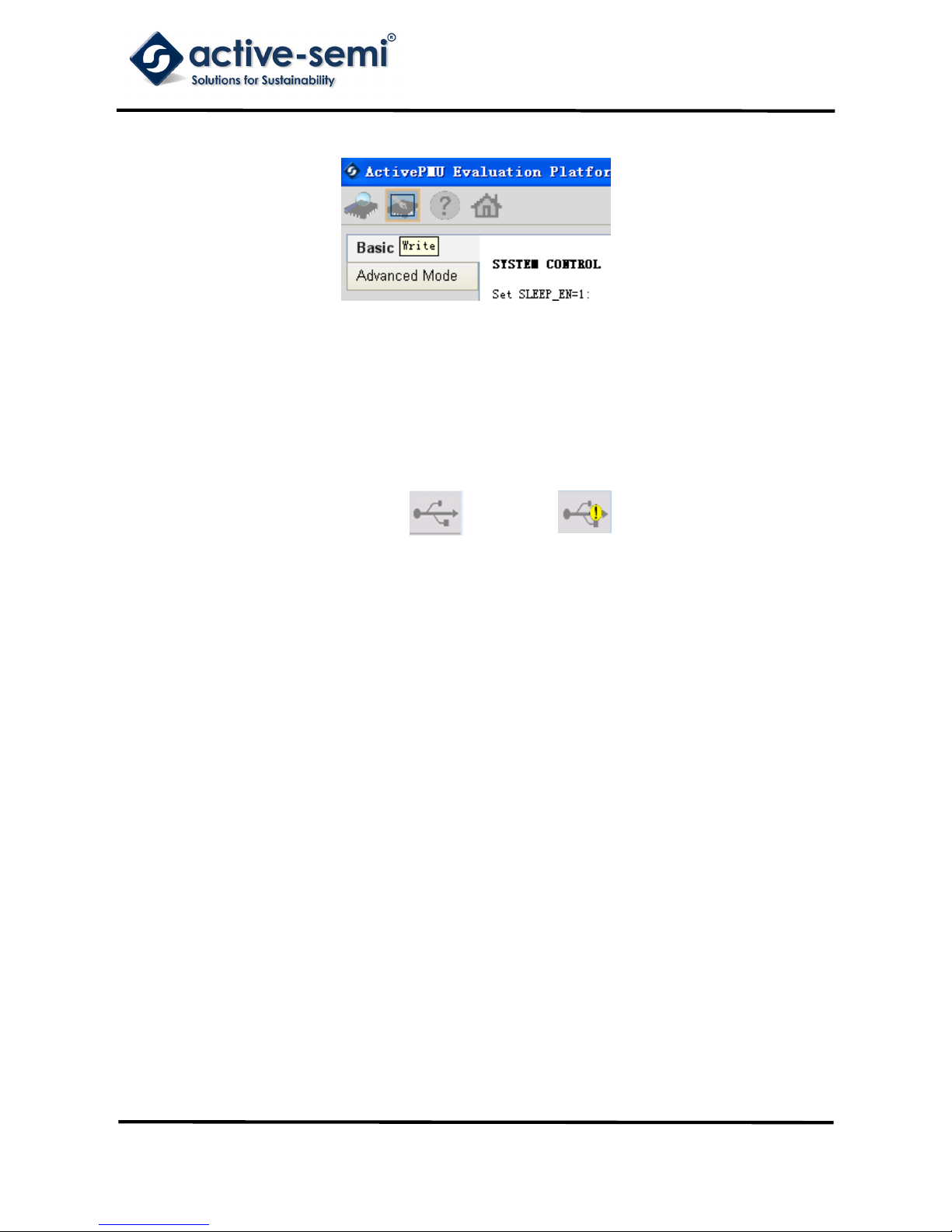
Dongle Connection Status: The GUI also contains a dongle is connected status which indicates that Active-
Semi’s USB-TO-I2C dongle is connected to the USB port of the driver installed. The figure below shows the two
possible indication status graphics.
Figure 16 – Dongle Connection Status
Dongle Dongle
Connected Disconnected
Table of contents
Other Active-semi Motherboard manuals


