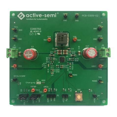
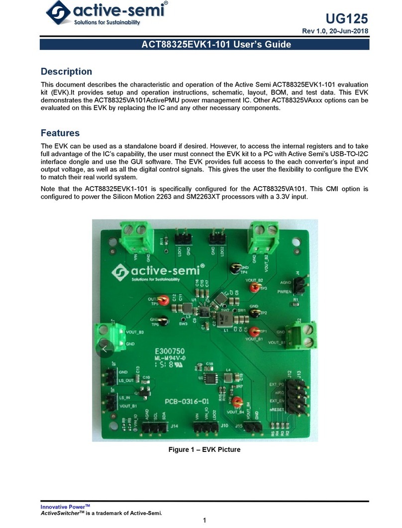
Active-semi ACT8865EVK1-305 User manual

UG109
Rev 3.0, 25-Sep-2018
Innovative Power
TM
ActiveSwitcher
TM
is a trademark of Active-Semi.
1
ACT8865EVK1-305 User’s Guide
Description
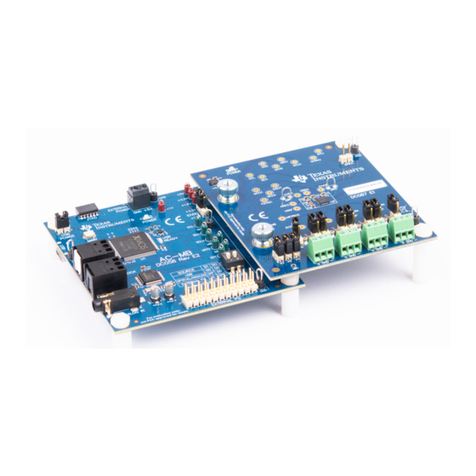
This document describes the characteristic and operation of the Active Semi ACT8865EVK1-305 evaluation kit
(EVK). It provides setup and operation instructions, schematic, layout, BOM, and test data. This EVK
demonstrates the ACT8865QI305 ActivePMU power management IC. Other ACT8865QIxxx options can be
evaluated on this EVK by replacing the IC and any other necessary components.
Features
The EVK can be used as a standalone board if desired. However, to access the internal registers and to take
full advantage of the IC’s capability, the user must connect the EVK kit to a PC with Active Semi’s USB-TO-I2C
interface dongle and use the GUI software. The EVK provides full access to the each converter’s input and
output voltage, as well as all the digital control signals. This gives the user the flexibility to configure the EVK
to match their real world system. The EVK features three step-down DC/DC converters and four low-noise, low-
dropout linear regulators. The three DC/DC converters utilize a high-efficiency, fixed-frequency (2MHz), current-
mode PWM control architecture that requires a minimum number of external components. Two DC/DCs are
capable of supplying up to 1150mA of output current, while the third supports up to 1300mA. All four low-dropout
linear regulators are high-performance, low-noise, regulators that supply up to320mA.Note that the
ACT8865AEVK1-305is specifically configured for the ACT8865QI305.
Figure 1 – EVK Picture

UG109
Rev 3.0, 25-Sep-2018
Innovative Power
TM
ActiveSwitcher
TM
is a trademark of Active-Semi.
2
Quick Start
Required Equipment
ACT8865EVK1-305
USB-TO-I2C Dongle
Power supply – 5V @ 3A for full power operation
Oscilloscope – >100MHz, 4 channels
Loads – Electronic or resistive. 2A minimum current capability.
Digital Multimeters (DMM)
Windows compatible computer with spare USB port.
E load
E load
PC
DC Power
E load
E load
USB dongle
Figure 2 – EVK Setup

UG109
Rev 3.0, 25-Sep-2018
Innovative Power
TM
ActiveSwitcher
TM
is a trademark of Active-Semi.
3
Hardware Setup
1. Connect a lab supply between Vin (J9) and GND (J10) to power all the regulators and LDOs.
2. Install shorting jumper on J1 to power REG4 and REG5.
3. Install shorting jumper on J2 to power REG6 and REG7.
4. Connect an appropriate load to each power supply output.
5. Note that the typical setup is to apply the same 5V input voltage to all inputs.
GUI Setup (optional)
1. Refer to the end of this document for detailed instructions to install the ACT8865 GUI.
2. Connect the USB-TO-I2C dongle to the computer via a USB cable.
3. Connect the USB-TO-I2C dongle to the EVK J13 connector. Refer to Figure 3 to ensure the correct
polarity of the connection. As a guide, use the “Active-Semi” logo on the top of the dongle so the black
wire is connected toward the lower left corner of the Dongle.
ACT8865
Figure 3 – USB-TO-I2C Dongle Connection
Turn On the Evaluation board
Before applying the input voltage, please make sure the jumper (J11) is installed.
When the power source and load are connected to the evaluation board, it can be powered for operation.
Perform the following steps to turn on the board.
1. Ensure that the power source voltage is >4.2V and <5.5V.
2. Ensure that nPBIN is not always low and monitor the output voltage from OUT1 to OUT7.
3. Turn on the load, check that it is drawing the proper load current, and verify that the output voltage maintains
its regulation.

UG109
Rev 3.0, 25-Sep-2018
Innovative Power
TM
ActiveSwitcher
TM
is a trademark of Active-Semi.
4
Recommended Operating Conditions
The ACT8865EVK1-305 is designed for a 5V input voltage. The maximum operating voltage is determined by
the IC’s maximum input voltage rating. The minimum operating voltages are determined by the buck converters’
minimum input voltage and by the LDOs’ dropout voltages. Maximum currents are determined by the IC’s CMI
settings, which can be changed via I2C after startup.
Table 1. Recommended Operating Conditions
Parameter Description Min Typ Max Unit
Vin All buck and LDO input voltages 2.7 5 5.5 V
I
out1_max
Maximum Buck REG1 load current 1.15 A
I
out2_max
Maximum Buck REG2 load current 1.15 A
I
out3_max
Maximum Buck REG3 load current 1.3 A
I
out4_max
Maximum LDO REG4 load current 0.32 A
I
out5_max
Maximum LDO REG5 load current 0.32 A
I
out6_max
Maximum LDO REG6 load current OFF A
I
out7_max
Maximum LDO REG7 load current OFF A
EVK Operation
Measuring Output Voltage Ripple
To observe the output voltage ripple, place the oscilloscope probe across the output capacitor with the probe
ground lead connected to the negative (-) capacitor terminal and the probe tip placed at the positive (+) capacitor
terminal. Set the oscilloscope to ac,5mV/division, 1us/division time base, and 20MHz bandwidth.
A standard oscilloscope probe has a long wire ground clip. For high frequency measurements, this ground clip
picks up high frequency noise and injects it into the measured output ripple. Figure 4 shows an easy way to
measure the output ripple properly. It requires removing the oscilloscope probe sheath and wrapping an
unshielded wire around the oscilloscope probe as short as possible, the true ripple can be measured.
Figure 4–Measuring output voltage ripple

UG109
Rev 3.0, 25-Sep-2018
Innovative Power
TM
ActiveSwitcher
TM
is a trademark of Active-Semi.
5
Test Load Transient Response
To test the load transient response, generate a load current transient at the output and observe the output
voltage response using an oscilloscope. Attach the current probe to the wire between the output and the load
to capture the current transient waveform. The method of testing the output voltage load transient response is
the same as that of testing output voltage ripple.
Measuring Efficiency
The Efficiency is measured by comparing the input power with the output power. Measure the input and output
voltage as close as possible to the input and output capacitor to reduce the effect of voltage drops in the PCB
and connectors.
Test Results
OUT5
OUT4
OUT3
OUT2
OUT1
CMI305 PWRHLDstartupsequence
2V/div
1V /d iv
2V /d iv
2V /d iv
5V/div
2ms/div
OUT6
OUT7
PWREN
20ms/div
5V/ d iv
0.5V/div
0.5V/div
PWRStartupSequence
0%
20%
40%
60%
80%
100%
0 200 400 600 800 1000 1200
Efficiency
OutputCurrentt(mA)
Efficiency@Vin=5V
OUT1
OUT2
OUT3

UG109
Rev 3.0, 25-Sep-2018
Innovative Power
TM
ActiveSwitcher
TM
is a trademark of Active-Semi.
6
OUT1
OUT2
OUT3
5mV/div
5mV/div
5mV/div
1us/div
OutputVoltageRipple
OUT1
IOUT1
20mV/div
1A/div
400 us/div
Load
Transient
OUT1=1.8V ,Iout=0A‐1.15A
LoadTransient
OUT2=1 .2V,Iout=0A‐1.15A
OUT2
IOUT2
20m V/div
1A/div
400us/div
OUT3
IOUT3
400us/div
50mV/div
1A/ div
LoadTransient
OUT3=3.3V,Iout=0A‐1.3A
OUT4
IOUT4
400 us/ div
50mV/div
200mA/div
LoadTransient
OUT4=2.5V,Iout=0A‐0.32A
OUT5
IOUT5
400 u s/ div
50mV/div
200 mA/ div
LoadTransient
OUT5=3.3V,Iout=0A‐0.32A

UG109
Rev 3.0, 25-Sep-2018
Innovative Power
TM
ActiveSwitcher
TM
is a trademark of Active-Semi.
7
40ms/div
OUT1
OUT2
nPBIN
nRSTO
2V/div
1V/div
5V/ div
5V/div
PressS1forlessthan130ms
OUT1
OUT2
nPBIN
nRSTO
100ms/div
2V/ div
1V/ div
5V/div
5V/div
PressS1formorethan130ms
PWRENisalwaysHigh
OUT1
100 ms/ d iv
2V/div
1V/div
5V/div
5V/div
PressS 1formorethan130ms
PWRENisalwaysLow
OUT2
nPBIN
nRSTO
nRSTO
nPBSTAT
nPBIN
5V/div
5V/div
5V/div
40m s/div
PressS2nPBINResistor=51kOhm

UG109
Rev 3.0, 25-Sep-2018
Innovative Power
TM
ActiveSwitcher
TM
is a trademark of Active-Semi.
8
Schematic
GND
1.5uHL3
GND
GND
GND
GND
GND
GND
GND
VIN
6.3V
4.7μF
C1
GND
GND
GND
OUT1
OUT2
OUT3
OUT4
OUT5
OUT6
OUT7
SW1
SW2
SW3
VDDREF
nPBIN
INL45
INL67
VIN
GND
TP16
VIN
REFBP
GND
GND
nRSTO
nIRQ
nPBSTAT
SCL
SDA
PWRHL D
PW RE N
VSE L
GND
GND
GND
GND
6.3V
4.7μF
C2
6.3V
4.7μF
C3
0R
R9
6.3V
100nF
C14
10K
R5
10K
R4
10K
R8
10K
R7
10K
R6
10K
R3
10K
R2
10K
R1
51K
R10
6.3V
47nF
C9
6.3V
2.2μF
C4
6.3V
2.2μF
C5
6.3V
22μF
C6
6.3V
22μF
C7
6.3V
22μF
C8
6. 3V
3.3μF
C10
6. 3V
3.3μF
C11
6. 3V
3.3μF
C12
6. 3V
3.3μF
C13
1.5uHL2
1.5uHL1
TP15
TP1
TP2
TP3
TP4
TP5
TP6
TP7
TP8
TP9
TP10
TP11
TP12
TP13
TP14
1
2
J9
1
2
J10
1
2
J11
1
2
J14
1
2
J15
1
2
J16
1
2
J17
2. 54
1
2
J3
1
2
J4
1
2J5
1
2J6
1
2J7
1
2
J8
1
2
J1
1
2
J2
1
2
3
J12
1
2
3
J13
GND
S1 S2 OUT1 1
AGND
2
OUT4 3
OUT5 4
INL45
5
INL67
6
OUT6 7
OUT7 8
nPBIN
9
PWRHL D
10
nRSTO
11
nIRQ
12
nPBSTAT
13
GP3 14
SW3 15
VP3
16
PW RE N
17
NC1
18
OUT3 19
VSE L
20
SCL
21
SDA
22
OUT2 24
VDDR E F
23
NC2
25
VP2
26
SW2 27
GP2 28
GP1 29
SW1 30
VP1
31
REFBP
32
EP 33
U1 ACT 8865
GND
GND
GND
GNDGND
VIN

UG109
Rev 3.0, 25-Sep-2018
Innovative Power
TM
ActiveSwitcher
TM
is a trademark of Active-Semi.
9
Layout
Figure 5 –Layout Assembly Layer

UG109
Rev 3.0, 25-Sep-2018
Innovative Power
TM
ActiveSwitcher
TM
is a trademark of Active-Semi.
10
Figure 6 –Layout Top Layer

UG109
Rev 3.0, 25-Sep-2018
Innovative Power
TM
ActiveSwitcher
TM
is a trademark of Active-Semi.
11
Figure 7 – Layout Layer 2

UG109
Rev 3.0, 25-Sep-2018
Innovative Power
TM
ActiveSwitcher
TM
is a trademark of Active-Semi.
12
Figure 7 – Layout Layer 3

UG109
Rev 3.0, 25-Sep-2018
Innovative Power
TM
ActiveSwitcher
TM
is a trademark of Active-Semi.
13
Figure 8 –Layout Bottom Layer

UG109
Rev 3.0, 25-Sep-2018
Innovative Power
TM
ActiveSwitcher
TM
is a trademark of Active-Semi.
14
Bill of Materials
Table 2. BOM list of EVK board
Item Ref Des QTY Description Package MFR Part Number
1 C1,C2,C3 3
Cap, Ceramic, 4.7uF,
6.3V, 10%, X7R 0805 std std
2 C4,C5 2
Cap, Ceramic, 2.2uF,
6.3V, 10%, X7R 0805 std std
3 C6,C7,C8 3
Cap, Ceramic,22uF,
6.3V, 10%, X7R 0805 std std
4 C9 1
Cap, Ceramic, 47nF,
6.3V, 10%, X7R 0603 std std
5 C10,C11,C12,C13 4
Cap, Ceramic, 3.3uF,
6.3V, 10%, X7R 0603 std std
6 C14 1
Cap, Ceramic, 100nF,
16V, 10%, X7R 0603 std std
7
J1,J2,J3,J4,J5,J6,J7,J
8,J9,J10,J11,J14,J15,
J16,J17 15 Header, 2 pin, 100mil
Wurth El-
ektronik 61300211119
8 J12,J13 2 Header, 3 pin, 100mil
Wurth El-
ektronik 61300211120
9 L1,L2,L3 3 Wurth inductor 1.5uH
4mmx4mmx
3.8mm
Wurth El-
ektronik 74438336015
10
R1,R2,R3,R4,R5,R6,R
7,R8 8 Res, 10kΩ, 1% 0603 std std
11 R9 1 Res, 0Ω, 1% 0603 std std
12 R10 1 Res, 51kΩ, 1% 0603 std std
13 S1,S2 2
SMT Tact switch
4mmx4mmx1.5mm 4x4x1.5 C&K
PTS525SK15SM
TR2LFS
14
TP1,TP3,TP5,TP7,TP
9,TP11,TP13,TP15 8
Test Point, Red,
Through Hole, 1mm 0.040" Keystone 5000
15
TP2,TP4,TP6,TP8,TP
10,TP12,TP14,TP16 8
Test Point, Black,
Through Hole, 1mm 0.040" Keystone 5001
16 U1 1 ACT8865QI305-T
4×4mm
TQFN44-32 std std
17 -- 1
PCB, ACT8865EVK1-
305 Rev A n/a n/a PCB-0308-00
18 -- 3 Jumper, 100mil, Black n/a
Wurth El-
ektronik 60900213421

UG109
Rev 3.0, 25-Sep-2018
Innovative Power
TM
ActiveSwitcher
TM
is a trademark of Active-Semi.
15
GUI Installation
1. Contact Active Semi for the GUI files and save them on your computer.
2. Plug the USB-TO-I2C dongle into a free USB port.
3. Follow the instructions in the “How to install driver for dongle” folder.
4. Double click on the ACT8865 GUI.exe to start the ACT8865 GUI.
GUI Overview
The GUI has 2 basic function buttons allocated in top-left of the Tool Bar which are Read and Write I2C. The
GUI contains 2 setting modes: Basic Mode and Advanced Mode. In Basic Mode screen it displays basic user
programmable configuration options are programmed using the drop-down boxes or check boxes. Advanced
Mode contain the button text for changing setting for every single bit.
Basic Mode
The following figure show the GUI in basic mode. This mode allows the user to easily change one or more IC
settings.

UG109
Rev 3.0, 25-Sep-2018
Innovative Power
TM
ActiveSwitcher
TM
is a trademark of Active-Semi.
16
Advanced Mode
Click the “Advanced Mode” button in the left of the GUI screen to see all available user programmable options.
With Advanced Mode, additional user programmable features can be selected using the button text. In the left
side of the Advanced Mode Screen, click on the Tiles Selector to display the register to view or change. Then
change a register one bit at a time by clicking on the desired bit. The value of the bit is display right next to the
bit-name button.
Note that the far right side of the screen contains a scroll down button to scroll down to additional registers since
the Tile Screen can only display up to 8 bytes at once.

UG109
Rev 3.0, 25-Sep-2018
Innovative Power
TM
ActiveSwitcher
TM
is a trademark of Active-Semi.
17
Button Descriptions
Read: Clicking on this button reads the ACT8865 registers and displays them in the GUI. Note that this reads
all registers. Active-Semi recommendsreading registers each time the ACT8865 powers-up to acquire the initial
register settings.Active-semi also recommends reading registers after making changes to them. Immediately
reading the registers after a write confirms the changes were properly stored.
Read Button
Write:Clicking on this button writes the GUI settings to the ACT8865’s registers. All registers are written,
regardless of whether or not they were changed.
Write Button
Dongle Connection Status: The GUI also contains a dongle is connected status which indicates that Active-
Semi’s USB-TO-I2C dongle is connected to the USB port of the driver installed. The figure below shows the two
possible indication status graphics.
Dongle connected
Dongle Disconnected
Table of contents
Other Active-semi Motherboard manuals
Popular Motherboard manuals by other brands
Texas Instruments
Texas Instruments TPS26620-23 user guide

Phytec
Phytec phyCORE-OMAP44 Series Quick start instructions
Linear Technology
Linear Technology DC2024A Demo Manual
Linear Technology
Linear Technology DC2125 Demo Manual

Analog Devices
Analog Devices EVAL-LT8641A-AZ Demo Manual
Analog Devices
Analog Devices DC2468A Demo Manual
