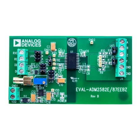
EVAL-LT8641A-AZ Demo Manual
65V, 3.5A/5A Peak Synchronous
Step-Down Silent Switcher
© 2023 Analog Devices, Inc. All rights reserved. Trademarks and registered trademarks are the property of their respective owners.
General Description
Evaluation circuit EVAL-LT8641A-AZ is a 65V, 3.5A/5A
peak synchronous step-down Silent Switcher®with
spread spectrum frequency modulation featuring the
LT®8641A. The demo board is designed for 5V output
from a 5.5V to 65V input. The wide input range allows a
variety of input sources, such as automotive batteries and
industrial supplies. The LT8641A is a compact, ultralow
emission, high efficiency, high speed synchronous
monolithic step-down switching regulator. Top and
bottom power switches, compensation components, and
other necessary circuits inside the LT8641A minimize
external components and simplify design. The special
Silent Switcher architecture minimizes EMI emissions.
The selectable spread spectrum mode can further
improve EMI performance. Ultralow 2.5μA quiescent
current in Burst Mode®operation achieves high efficiency
at very light loads. Fast minimum on-time of 35ns enables
high VIN to low VOUT conversion at high frequency.
The LT8641A switching frequency can be programmed
either through oscillator resistor or external clock over a
200kHz to 3MHz range. The default frequency of the
evaluation board is 2MHz. The SYNC pin on the
evaluation board is grounded by JP1 for low ripple burst
mode operation. Move JP1 to PULSE SKIPPING position
to change the operation mode to pulse-skipping
operation. Once JP1 is on SPREAD SPECTRUM
position, VCC is applied to the SYNC pin for low EMI
spread spectrum operation. To synchronize to an external
clock, move JP1 to SYNC and apply the external clock to
the SYNC turret. Figure 1 shows the efficiency of the
circuit at 12V and 24V input in Burst Mode operation.
Figure 2 shows EMI performances of the board (with EMI
filter). The red lines in Figure 2 are CISPR25 Class5 peak
limit. The figure shows that the circuit passes the test with
a wide margin. To achieve EMI/EMC performance, as
shown in Figure 2, the input EMI filter is required, and the
input voltage should be applied at the VEMI turret.
The LT8641A data sheet gives a complete description of
the part, operation, and application information. Read the
data sheet in conjunction with this user guide for EVAL-
LT8641A-AZ. The LT8641A is assembled in a 3mm × 4mm
plastic QFN package with exposed pad for low thermal
resistance. The layout recommendations for low EMI
operation and maximum thermal performance are
available in the “Low EMI PCB Layout and Thermal
Considerations” and “Peak Output Current” sections of the
data sheet.
Performance Summary Specifications are at TA= 25°C
VIN = 12V, IOUT = 0A to 3.5A
Maximum Continuous
Output Current
VIN = 12V, fSW = 2MHz,
VOUT = 5V, IOUT = 1A
