adesto SM2400 EVK User manual

UG-SM2400–-156B–-10/2018
SM2400 Evaluation Kit
User’s Guide
Communication Technology by:
Semitech Semiconductor

2SM2400 EVK User’s Guide
UG-SM2400–-156B–-10/2018
This publication contains proprietary information which is subject to change without notice and is supplied ‘as
is’, without any warranty of any kind.
Revision History
Revision Number Date Tasks
A 7/2016 SM2400 Evalua ion Ki User’s Guide ini ial release.
B 10/2018 Thorough echnical edi of exis ing ma erial, Added new ma erial or clarified
exis ing ma erial where necessary.
Change documen number from UG-SM2400EVK1A-PWRLN o
UG-SM2400-156

3SM2400 EVK User’s Guide
UG-SM2400–-156B–-10/2018
Table of Contents
1. In roduc ion .....................................................................................................................................4
2. EVK Fac ory Configura ion Op ions ................................................................................................4
3. Package Con en s ..........................................................................................................................4
4. SM2400 EVK Sys em Overview .....................................................................................................5
4.1 SM2400 EVK Hardware Configura ion ....................................................................................5
4.2 SM2400 Firmware ...................................................................................................................6
5. SM2400 EVK Hardware Componen s ............................................................................................7
5.1 IEC Connec or .........................................................................................................................7
5.2 Mini-USB Connec or ................................................................................................................7
5.3 Rese Bu on ............................................................................................................................8
5.4 Ex ernal DC Power Supply ......................................................................................................8
5.5 Combining an MCU and SM2400 ............................................................................................9
5.5.1 UART In erface on H11 .................................................................................................10
5.5.2 SPI In erface on Connec or H11 ...................................................................................11
5.5.3 RS232 In erface on H13 ...............................................................................................12
6. Evalua ion and Se up ....................................................................................................................17
6.1 General Se up and Connec ion .............................................................................................17
6.2 Evalua ion wi h PRIME ..........................................................................................................18
6.2.1 Program PRIME PHY ...................................................................................................18
6.2.2 Evalua e PRIME PHY ...................................................................................................19
6.2.3 Evalua e PRIME Ne work .............................................................................................22
6.3 Evalua e G3-PLC ..................................................................................................................38
6.3.1 Program G#_PLC PHY .................................................................................................38
6.3.2 Evalua e G3-PLC PHY ..................................................................................................38
6.3.3 Evalua e G3-PLC MAC .................................................................................................41
6.4 Evalua e IEEE FCC PHY ......................................................................................................47
6.4.1 Program IEEE FCC PHY ..............................................................................................47
6.4.2 Tes IEEE FCC PHY .....................................................................................................47
6.4.3 Tes IEEE FCC MAC ....................................................................................................49
6.5 Evalua ion wi h XR (NOFDM) Mode ......................................................................................49
6.5.1 Program XR PHY ..........................................................................................................49
6.5.2 Tes XR PHY .................................................................................................................49
6.5.3 Evalua e XR wi h SMesh MAC .....................................................................................51
6.6 Evalua ion wi h XXR Mode ....................................................................................................51
6.6.1 Program XXR Mode Firmware ......................................................................................51
6.6.2 Tes XXR PHY ..............................................................................................................51
6.6.3 Evalua e XXR wi h SMesh MAC ...................................................................................53
6.7 Evalua e CEN-B/C .................................................................................................................56
6.7.1 Evalua e CEN-B/C PHY ................................................................................................56
6.7.2 Evalua e CEN-BC MAC ................................................................................................56
6.8 Troubleshoo ing .....................................................................................................................56
6.8.1 Problem — Canno Connec o he Serial Por of he PC .............................................56
6.8.2 Problem — Can' Receive Any Packe s ........................................................................56
6.8.3 Analyzing he Power Line Condi ion using Channel Moni or ........................................57
6.8.4 Check he Raw Packe Da a from he Command Log ..................................................60

4SM2400 EVK User’s Guide
UG-SM2400–-156B–-10/2018
1. Introduction
The SM2400 Evalua ion Ki (EVK) is an evalua ion ki for he SM2400 universal Narrowband Power Line Communica ion (N-
PLC) modem. The SM2400 EVK is designed o evalua e and develop various SM2400-based N-PLC solu ions, including all
major OFDM based N-PLC s andards, such as PRIME, G3-PLC and IEEE 1901.2, as well as proprie ary modes by loading
differen firmware versions.
The SM2400 EVK includes a PC-based GUI applica ion (SM2400Control.exe) ha enables comprehensive configura ion
and con rol of he SM2400 modem and moni oring/ es ing of he communica ion performance.
Fea ures of he SM2400 EVK include:
• A comple e N-PLC node solu ion wi h no ex ernal componen s needed
• Mini USB connec ion for bo h UART and SPI in erface o he SM2400 PLC ransceiver as well as direc UART
connec ion
• IEC C7 power connec ion
• Buil -in power line coupling circui
• Abili y o bypass on-board swi ched-mode power supply and use ex ernal DC supply o implemen PLC
connec ion on cold wires
• LED indica ors for ransmi and receive
• Programmable PRIME/G3-PLC/IEEE 1901.2/XR/XXR firmware
• JTAG debugging
2. VK Factory Configuration Options
The EVK can be fac ory-configured wi h he numerous line driver and frequency band op ions. For each Ades o par number,
he las wo charac ers indica e he line driver and frequency band used. For example, SM2400-EVK1M1-A. In his case, he
number 1 and he le er A will change based on he line driver and frequency band used. The SM2400 EVK suppor s all
combina ions shown in Figure 1.
Figure 1. VK Factory Configuration Options
3. Package Contents
Each SM2400 EVK con ains:
• 1 x SM2400-EVK1 base board
• 1 x SM2400-EV1Mn-A or 1 x SM2400-EV1Mn-B or 1 x SM2400-EV1Mn-C module board — The ‘n’ in he par
number refers o he line driver and can be a value of 1, 2, or 3. Refer o Figure 1 for more informa ion.
• SM2400 N-PLC ransceiver (loca ed on he module board)
• 1 x mini USB cable
No e: A leas wo SM2400 EVK’s are needed for power line communica ion evalua ion.
SM2400-EVK1Mn-x
1 = Texas Ins rumen s Line Driver
2 = In ersil Line Driver
3 = Discre e Line Driver
A = CEN-A Frequency Band
B = CEN-B/BC Frequency Band
C = FCC Frequency Band

5SM2400 EVK User’s Guide
UG-SM2400–-156B–-10/2018
4. SM2400 VK System Overview
The SM2400 N-PLC ransceiver is loca ed on he SM2400-EV1Mn-x module board as shown in Figure 2. The SM2400-
EV1Mn board con aining he SM2400 N-PLC device is connec ed o he SM2400-EVK1 base board o comprise he SM2400
Evalua ion Ki (EVK).
Figure 2. SM2400 VK Components (Top View)
From ime o ime new firmware packages are released ha demons ra e new fea ures and applica ions, such as Serial- o-
PLC adap er. The SM2400 EVK includes a PC-based GUI applica ion (SM2400Control.exe) ha enables comprehensive
configura ion and con rol of he SM2400 modem and moni oring/ es ing of he communica ion performance.
This documen describes he SM2400 EVK and he SM2400Control GUI sof ware.
4.1 SM2400 VK Hardware Configuration
The SM2400 EVK consis s of wo boards:
1. The SM2400 EVK1 base board con ains a swi ched-mode power supply module, PLC module connec or,
communica ion in erface (USB), and a rese bu on.
2. The SM2400-EV1 PLC module includes he SM2400 device, as well as SPI Flash memory, an Analog Fron -End (AFE)
circui , and a coupling circui . The module comes wi h one he following op ions depending on he desired opera ional
band:
• The SM2400-EV1Mn-A includes an in egra ed power amplifier and a coupling circui for he CENELEC A band.
The ‘n’ in he par number refers o he line driver. Refer o Figure 1 for more informa ion.
• The SM2400-EV1Mn-B includes an in egra ed power amplifier and a coupling circui for he CENELEC B and C
bands.
• The SM2400-EV1Mn-C includes an in egra ed power amplifier and coupling circui for he FCC band.
SM2400-EVK1
SM2400-EV1Mn-x

6SM2400 EVK User’s Guide
UG-SM2400–-156B–-10/2018
The above modules are used as an example hroughou his documen . From ime o ime Ades o releases addi ional
varian s of he module wi h differen par numbers ha use al erna ive power amplifiers (Line Drivers), which can also be
used in conjunc ion wi h he SM2400-EVK1Mn base board wi hou any o her changes o he se up.
The PC in erface o he SM2400 EVK is hrough a s andard mini-USB connec or. A s andard IEC C7 plug is used as he
main power connec or o accommoda e differen ypes of main ou le s.
Typically, in order o demons ra e communica ion over a power line, wo SM2400 EVK’s are required. The wo EVK’s can
communica e wi h each o her by bo h connec ing o he same power line, as illus ra ed in Figure 3. Each EVK is connec ed
via a USB por o a PC running he SM2400Control applica ion. The applica ion is used o con rol and moni or he
communica ion. To communica e properly, bo h EVK’s mus be running he same firmware load (PHY and pro ocol). Refer
o he following sec ion for a lis of firmware loads.
No e ha he SM2400 EVK can also be used o es in eroperabili y wi h o her devices. In such cases, one EVK is sufficien .
I mus be connec ed o he same power line as he o her devices and run he same pro ocol (e.g. PRIME or G3-PLC).
Figure 3. Multiple SM2400 VK Connections
4.2 SM2400 Firmware
Since he SM2400 N-PLC ransceiver suppor s many communica ion schemes, he SM2400 EVK is offered wi h differen
firmware loads ha suppor various communica ion schemes and pro ocols. Each offering is a separa e firmware version
ha can be downloaded o he SPI Flash available on he EVK via he USB cable using he SM2400Control GUI sof ware.
The SM2400Control GUI can also be used as he con roller o allow evalua ion and debugging as well as early sys em
in egra ion. The firmware loads are independen of any EVK specifics and are even ually used in he final produc s wi hou
any changes.
The SM2400 EVK firmware offerings include PRIME PHY, PRIME MAC, G3 PHY, G3 MAC, and XXR modes, and IEEE
1901.2 high-band (FCC) PHY and MAC. From ime o ime new firmware packages are added ha implemen new schemes
or applica ions.
The SM2400 EVK firmware versions suppor all major OFDM s andards including PRIME, G3-PLC and IEEE 1901.2 high-
band as well as he robus proprie ary XR and XXR modes. Each s andard and proprie ary mode is ypically available in he
following configura ions o allow differen levels of es ing:
• PHY only for easies se ing and performance evalua ion
• PHY+ MAC ha enables es ablishing and evalua ing ne work performance
• PHY+ ADP ha also includes Adap a ion Layer for a comple e applica ion
Las ly, each communica ion scheme is ypically available for differen opera ional bands, such as, CEN-A or FCC.
Below is a comple e lis of he firmware versions available for he SM2400 EVK. From ime o ime Ades o releases addi ional
firmware versions for new s andards and communica ion modes.
SM2400 VK #1
SM2400 VK #2

7SM2400 EVK User’s Guide
UG-SM2400–-156B–-10/2018
5. SM2400 VK Hardware Components
There are a few ex ernal connec ors ha can be used o in erface o he SM2400 EVK.
5.1 I C Connector
The IEC C7 plug is used o connec he SM2400 EVK o he power line. This plug is connec ed o bo h he on-board swi ch
mode AC-DC power supply and he coupling circui . Looking in o he connec or, he righ pin is neu ral and lef pin is line/
ac ive as shown in Figure 4.
Figure 4. SM2400 VK I C Connector
5.2 Mini-USB Connector
The mini-USB connec or is used o connec a hos (i.e. PC) o he SM2400 EVK. The PC connec s o he mini-USB connec or
o access he SM2400EVK via an on-board USB- o-serial conver er. The mini-USB connec or (UART) is shown in he
Figure 5.
Table 1. SM2400 VK Firmware Versions
PRIME PHY (CEN A) IEEE 1901.2 PHY + MAC (CEN-B)
PRIME PHY + MAC (CEN A) IPv4 IEEE 1901.2 PHY + ADP (CEN-B)
PRIME PHY + MAC (CEN A) IPv6 IEEE 1901.2 PHY (CEN-C)
G3-PLC PHY (CEN A) IEEE 1901.2 PHY + MAC (CEN-C)
G3-PLC PHY + MAC (CEN A) IEEE 1901.2 PHY + ADP (CEN-C)
G3-PLC PHY + ADP (CEN A) IEEE 1901.2 PHY (CEN-BC)
G3-PLC PHY (FCC) IEEE 1901.2 PHY + MAC (CEN-BC)
G3-PLC PHY (FCC) IEEE 1901.2 PHY + ADP (CEN-BC)
G3-PLC PHY + MAC (FCC) IEEE 1901.2 PHY (FCC)
G3-PLC PHY + ADP (FCC) IEEE 1901.2 PHY + MAC (FCC)
IEEE 1901.2 PHY (CEN-A) IEEE 1901.2 PHY + ADP (FCC)
IEEE 1901.2 PHY + MAC (CEN-A) XXR PHY
IEEE 1901.2 PHY + ADP (CEN-A) XXR PHY + SMESH
IEEE 1901.2 PHY (CEN-B)
Line Neu ral

8SM2400 EVK User’s Guide
UG-SM2400–-156B–-10/2018
5.3 Reset Button
The rese bu on is loca ed beside he mini-USB connec or as shown in Figure 5.
Figure 5. SM2400 VK Reset Button and UART Connector
5.4 xternal DC Power Supply
The SM2400 EVK can be powered by ei her he on-board swi ch mode AC power supply or by an ex ernal 15V/1A plug pack
o 2.1mm DC plug H1. Swi ch S2 shown in Figure 6 is used o choose which supply source (AC or DC) will be used by he
SM2400 EVK.
The DC-DC conver er circui s consis of a swi ching (U6) and a linear regula or (U14) o provide he required 3.3V power
supply up o 1A for all digi al and analog par s. The firs s age of cascaded regula ors is he 5V swi ching regula or ha has
been used for high efficiency, wide inpu range and also accura e ou pu vol age regula ion o drop mos of he vol age (15V
o 5V) and hen U14 as he 3.3V linear regula or provides low ripple, low noise on he DC power rails o keep signals from
being so noisy.
Rese mini-USB (UART)

9SM2400 EVK User’s Guide
UG-SM2400–-156B–-10/2018
Figure 6. SM2400 VK AC/DC Power Supply Switch
The in erface header H7 on he base board and he PLC module as can bee seen in Figure 7 suppor s he AFE_VCC as he
line driver power supply (15V@1A) and 3.3V (3.3V@1A) for he SM2400.
Figure 7. DC Power Supplies on H7 Connector
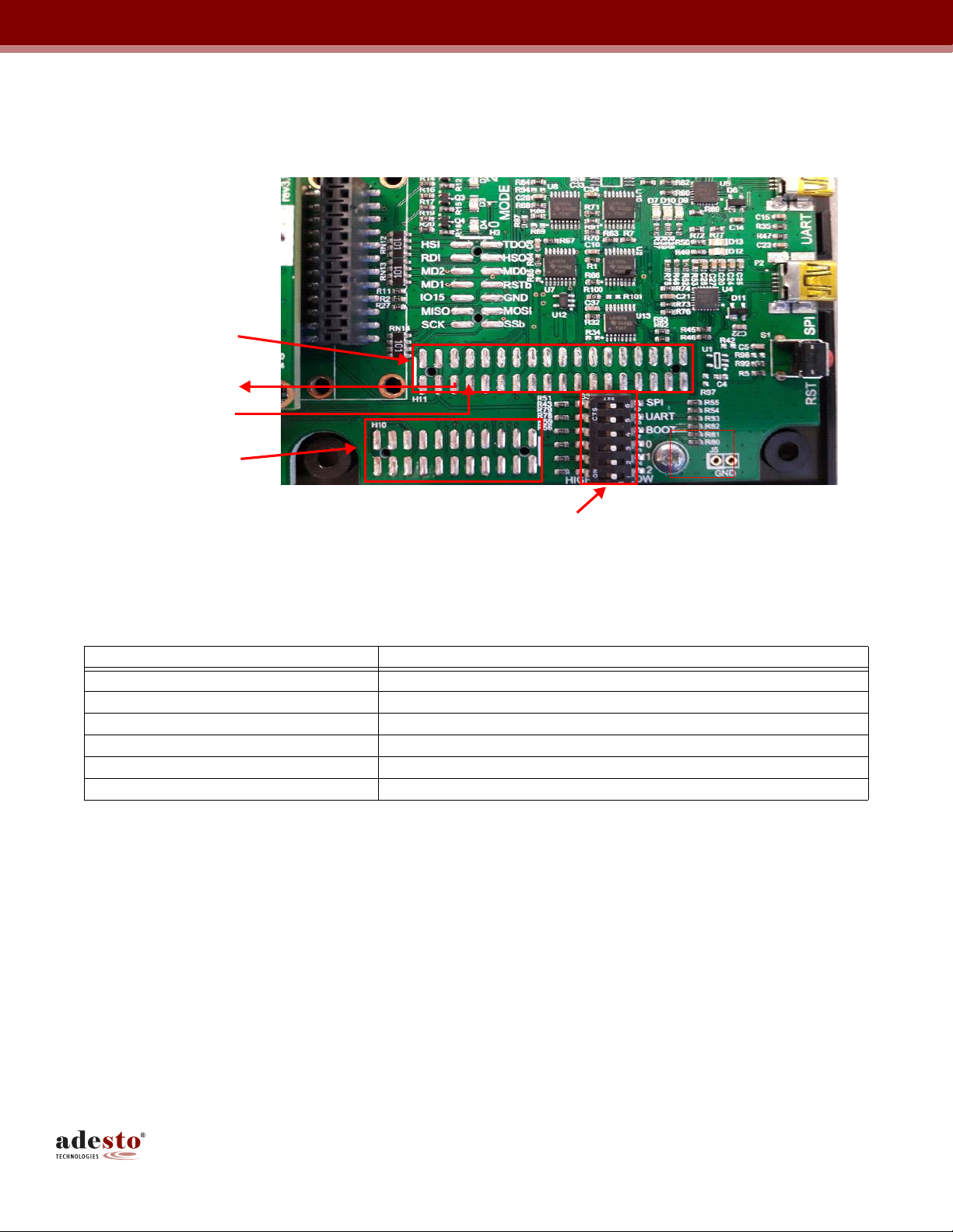
5.5 Combining an MCU and SM2400
The SM2400 EVK has been designed o be easily managed by an ex ernal microcon roller hrough differen ype of
in erfaces, including SPI, UART and RS232. Selec ing he in erface ype can be con rolled ei her via he S3 manually or via
he con rol pins on he H11 connec or. The following sec ion explains how o configure he SM2400 EVK for an ex ernal MCU
connec ion manually, however embedded developers can follow he same ins ruc ions o configure he same con rol pins as
on he H11 in heir codes.
S2: AC/DC Power Supply Swi ch
10SM2400 EVK User’s Guide
UG-SM2400–-156B–-10/2018
5.5.1 UART Interface on H11
An MCU can be connec ed o he SM2400-EVK1 baseboard via he hos in erface H11 connec or o provide con rol hrough
he UART_TDO (H11 pin 5) and he UART_RDI (H11 pin 7) as shown in Figure 9.
Figure 8. UART Connection to a Host MCU
The UART mode is configured using he DIP swi ch S3 se ings in Table 2.
Refer o Figure 9 below for he comple e pin lis of he H11 connec or pins.
Table 2. S3 Switch Select for the UART Interface on H11
S3 Switch Number Value
6 (SPI_SEL) Low.
5 (UART_SEL) High.
4 (BOOT_SEL) High.
3 (MODE2) As described in Table 8 for differen boo modes.
2 (MODE1) As described in Table 8 for differen boo modes.
1 (MODE0) As described in Table 8 for differen boo modes.
SM2400_TDO
SM2400_RDI
1
2
H11 Connec or
H10 Connec or
DIP Swi ch S3

11SM2400 EVK User’s Guide
UG-SM2400–-156B–-10/2018
Figure 9. H11 Pin List
5.5.2 SPI Interface on Connector H11
The da a exchange be ween he MCU and SM2400 EVK can be done hrough he SPI in erface on he H11 if he S3 DIP
swi ches are configured as shown in Table 3. The chosen MCU mus have an SPI in erface and a sufficien amoun of in ernal
RAM (>= 4KB). The SPI in erface signals on H11 are as follows:
• SPIS_OUT: H11 (pin 27)
• SPIS_SCK: H11 (pin 29)
• SPIS_SSb: H11 (pin 31)
• SPIS_IN: H11 (pin 27)
• COREIO15: H11 (pin 35). This pin can be used as an in errup signal ha is riggered when he SM2400 is sending or
receiving da a.
Table 3. S3 Switch Select for the SPI Interface on H11
S3 Switch Number High/Low
6 (SPI_SEL) High.
5 (UART_SEL) Low.
4 (BOOT_SEL) High.
3 (MODE2) As described in Table 8 for differen boo modes.
2 (MODE1) As described in Table 8 for differen boo modes.
1 (MODE0) As described in Table 8 for differen boo modes.

12SM2400 EVK User’s Guide
UG-SM2400–-156B–-10/2018
Figure 10. SPI Interface Timing Diagram
5.5.3 RS232 Interface on H13
An user MCU can also be connec ed o he SM2400-EVK1 baseboard via he RS232 in erface H13 o con rol he SM2400
EVK when he S3 DIP swi ches are configured as shown in Table 4. Refer o Table 5 for he comple e pin lis of H13 and
Figure 11 for he foo prin of H13.
No e ha in some boards he H13 header and associa ed componen s U9, C29, C30, C31, C32, and C33 are no popula ed.
These are readily available and can be moun ed if needed (H13: TSM-105-01-L-DV-A, U9: SP3232EBEY-L, C29-C33: 1uF).
Table 4. S3 Switches Select for the UART Interface on H11
S3 Switch Number High/Low
6 (SPI_SEL) Low.
5 (UART_SEL) Low.
4 (BOOT_SEL) Low.
3 (MODE2) As described in Table 8 for differen boo modes.
2 (MODE1) As described in Table 8 for differen boo modes.
1 (MODE0) As described in Table 8 for differen boo modes.
Table 5. H13 Pin List
Pin Number Name
1, 2 N/C
3 RS232_TXDO
4 RS232_HSI
5 RS232_RXDI
6 RS232_HSO
7, 8 N/C
9 GND
10 N/C

13SM2400 EVK User’s Guide
UG-SM2400–-156B–-10/2018
Figure 11. RS232 Connection
Multiplexing of the SM2400- VK1 Baseboard
The S3 swi ches enable boo ing up from a hos MCU or from a Flash residing on he module and i also enable
communica ing SM2400 EVK via USB UART/SPI or hos UART/SPI. For normal opera ion (boo from SPI Flash), ensure
ha all he swi ches of S3 are swi ched o LOW posi ion as shown in Figure 12.
Figure 12. SM2400- VK1 S3 Switch Selection
Refer o Table 6 for he comple e lis of S3 mul iplexed signals. The HIGH/LOW s a e for each swi ch is no ed on he silk
screen as shown in he figure above.
RS232_TXDO
RS232_RXDI
U9
S3
14SM2400 EVK User’s Guide
UG-SM2400–-156B–-10/2018
The whole mul iplexing of he SM2400-EVK1 Baseboard is illus ra ed in Figure 13.
Figure 13. Multiplexing of the SM2400- VK1 Baseboard
For example, when using SM2400Control GUI o con rol he SM2400 EVK via he defaul USB UART in erface and boo
from he SPI Flash on he SM2400-EV1Mn module, se all six S3 swi ches o low. In he case of using an ex ernal Hos UART
(via H11) o con rol SM2400-EV1Mn and boo from he Hos UART, se S3 (5), S3 (4) and S3 (2) o high and res o low. In
he case of using an ex ernal RS232 Hos UART (via H13) o con rol he SM2400 N-PLC ransceiver and boo from he SPI
Flash, se S3 (2) o high and res o low and unplug he mini-USB cable from he USB UART (P1) por .
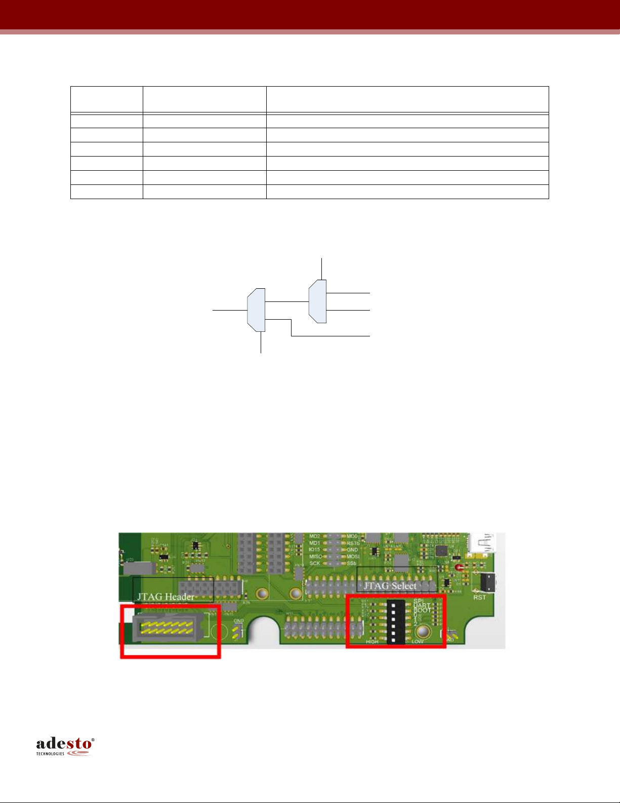
JTAG Debug Operation
The SM2400-EVK1 base board suppor s JTAG debugging. The area of he board ha is rela ed o JTAG con rol is
highligh ed in Figure 14.
Figure 14. JTAG Control Regions of the SM2400- VK1 Board
Table 6. S3 Select Switches
S3 Switch
Number
Name Description
6 HOST_SPI CP2130_SPI
5 HOST_UART (H11) CP2110_UART/ RS232_UART (H13)
4 HOST_BOOT CP2110_BOOT
3 '1” HOST_MODE0
2 '1” HOST_MODE1
1 '1” HOST_MODE2
00
11
SM2400_UART
RS232_UART (H13)
USE_UART (P1)
HOSTUART (H11)
S3_5
MiniUSB_cable

15SM2400 EVK User’s Guide
UG-SM2400–-156B–-10/2018
JTAG Header
A 14 pin connec or is provided o connec a JTAG probe. The key signals are shown in Figure 15 and de ailed in Table 7. A
compa ible probe needs o be used.
Figure 15. JTAG Header Pin Out
JTAG Select
To opera e in JTAG debug mode, he mul iplexor mus be pu in he respec ive mode. The bes way is o opera e
in manual boo ing mode. This is done by se ing S3 (6) LOW, S3 (5) LOW and S3 (4) HIGH, as shown in
Figure 16.
No e ha he manual boo ing mode, as sugges ed above, assures ha he MODE[2:0] pins canno be changed
in run ime by he GUI hrough he USB o UART/SPI in erface. The la er capabili ies is used during
programming, bu is no desired during normal opera ion.
Table 7. JTAG Header Signals
Pin Description
1 JTDI
2 GND
3 JTDO
4 GND
5 JTCK
6 GND
7 N/A
8 N/A
9 RESETb
10 JTMS
11 JTAG_TVcc
12 GND
13 N/A
14 JTRSTb

16SM2400 EVK User’s Guide
UG-SM2400–-156B–-10/2018
Figure 16. Multiplexer Settings for Host Interface, Boot Mode Selection and JTAG Operation
Once in manual mode, he boo selec or swi ches can be se o he desired mode. For DLL JTAG debugging, his
would have all 3 swi ches se HIGH. All modes are lis ed in Table 8.
(*) “Boo from ex ernal memory” is no relevan for SM2400 based (SM2400-EV1Mn-x1) modules.
Table 8. ncoding of S3 Switches 1 - 3 to Select Different Boot Modes
S3 (1) S3 (2) S3 (3) Mode
0 0 0 Boo from SPI FLASH
0 0 1 Boo from Hos SPI
0 1 0 Boo from Hos UART
0 1 1 Boo from ex ernal memory *
1 0 0 Reserved
1 0 1 Reserved
1 1 0 DLL and PHY JTAG Debug mode
1 1 1 DLL JTAG Debug mode
1. Mn-x — Refer o Figure 1 for he defini ion of ‘n’ and ‘x’.
Boot selectors
Manual Mode
Settings

17SM2400 EVK User’s Guide
UG-SM2400–-156B–-10/2018
6. valuation and Setup
6.1 General Setup and Connection
The ins ruc ions below describe he general se up for a SM2400-EVK1M1 applica ion.
The SM2400 EVK was designed o help es ing and evalua ing he fea ures and capabili ies of he SM2400 N-
PLC modem using he SM2400Control GUI.
For PRIME or G3-PLC CENELEC-A band, evalua ion ensures ha he SM2400-EV1Mn-A modules for
CENELEC-A band are used.
For G3-PLC CENELEC-B band or IEEE 1901.2 CENELEC-B band evalua ion ensure ha he
SM2400-EV1Mn-B modules for CENELEC-B band are used.
For G3-PLC FCC or IEEE 1901.2 FCC evalua ion ensure ha he SM2400-EV1Mn-C modules for FCC band are
used. XR and XXR modes can be configured o opera e in any of he bands.
Plug bo h EVK’s o he same power-line and connec wo SM2400 EVK boards o wo PC’s hrough USB cables
as shown in Figure 3.
S ar he SM2400Control GUI applica ion by double clicking he execu able file. Upon running he program, he
following window is displayed:
Figure 17. SM2400Control Main Display Window
The SM2400 EVK can be au oma ically connec ed o he serial por hrough he on-board CP2110 HID USB TO
UART BRIDGE. Once i is connec ed, he serial number of he CP2110 on he EVK is shown on he op of GUI
menu bar and under he Dev Board ab.

18SM2400 EVK User’s Guide
UG-SM2400–-156B–-10/2018
Figure 18. Locating the Serial Number (Red Box in Figure)
If he EVK is no au oma ically connec ed, click Scan o find he CP2110 serial number, and hen click Connec .
6.2 valuation with PRIM
6.2.1 Program PRIM PHY
Before evalua ing he SM2400 PRIME PHY, make sure ha he la es version is presen on he EVK. To
download/upgrade he PRIME PHY firmware of SM2400 EVK using he SM2400Control GUI via he USB cable
follow he following s eps:

19SM2400 EVK User’s Guide
UG-SM2400–-156B–-10/2018
1. Click he Flash ab. The following screen sho is displayed.
2. Browse o find he firmware (i.e. img-pass hru-prime-evk2_opa564-vxxx.bundle) provided.
3. Click Program Flash.
4. Wai un il he Programming Completed Successfully message is displayed.
6.2.2 valuate PRIM PHY
Af er downloading he PRIME pass- hrough firmware o bo h EVK’s, under he Configuration ab, click he Reset
bu on o ge he Mode o PRIME, if i is no au oma ically se .
One node should be configured as he ransmi er (Tx) and he o her as he receiver (Rx).
1. Click x est o se he firs GUI/EVK as Tx node. The SM2400Control GUI allows for a number of op ions o be
configured for he Tx node as follows:
• Se Transmi Level (from highes level 0dB o lowes level -21dB).
• Se Modula ion (BPSK/QPSK/8PSK).

20SM2400 EVK User’s Guide
UG-SM2400–-156B–-10/2018
• Enable FEC (Forward Error Correc ion) — Should always be enabled.
• Wri e he number of packe s o be sen from Tx Tes ab (0 means con inuously sending packe s wi hou s op).
• Change he packe size if needed.
• Se Da a pa ern.
Click he Start est bu on on he Tx Tes ab from he Tx window and moni or he resul s from he Rx Tes ab
from he Rx window as shown in he following screen sho .
2. Se he second GUI/EVK as Rx node.
• Check if he 2nd EVK is connec ed o he GUI.
• Download he PRIME firmware o he 2nd EVK.
• Click he Rx est ab as shown in Figure 19.
• When he Tx node is ransmi ing packe s, he resul s (e.g. received packe s) should be au oma ically displayed
on he GUI of he Rx EVK.
• Click Plo Resul s bu on as shown in Figure 20 o ge a bar char of he received packe s, SNR and RSSI
values.
• Click Clear Resul s if needed.
Table of contents
Other adesto Motherboard manuals


