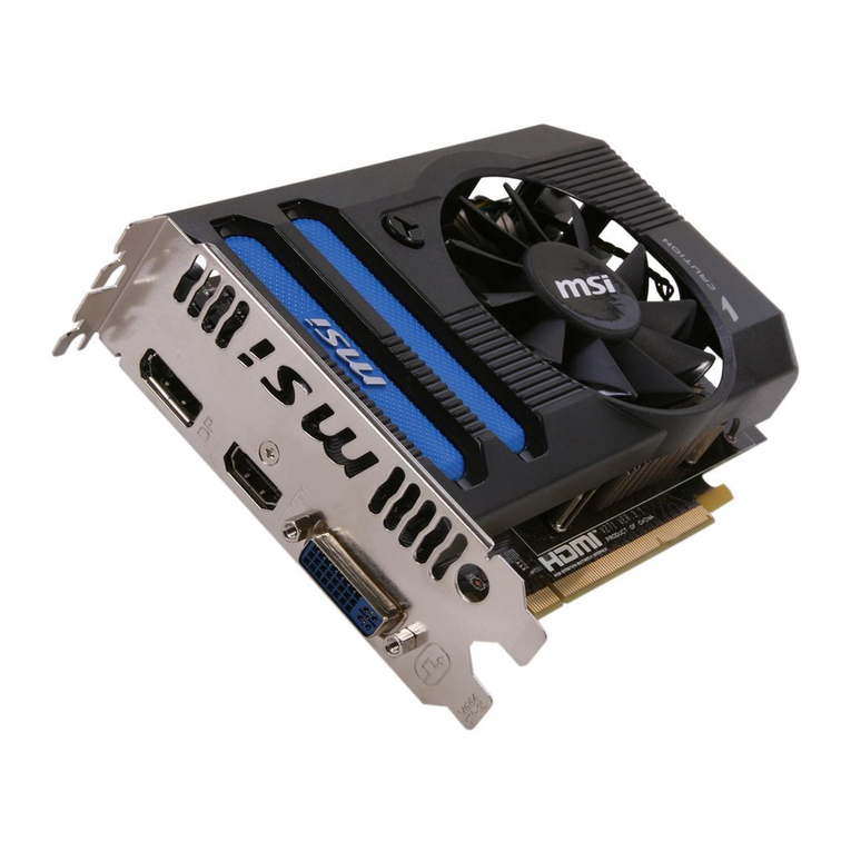
ADLINK Technology EGX-MXM-A4500 User manual

EGX-MXM-A4500
NVIDIA Ampere™ GA104 RTX A4500
Embedded Graphics Module
User’s Manual
Manual Rev.: 1.0
Revision Date: Oct. 16, 2022
Part No: 50M-00094-1000

ii Revision History
Leading EDGE COMPUTING
Revision History
Revision Release Date Description of Change(s)
1.0 2022-10-16 Initial release

Preface iii
EGX-MXM-A4500
Preface
Copyright © 2022 ADLINK Technology Inc.
This document contains proprietary information protected by copy-
right. All rights are reserved. No part of this manual may be repro-
duced by any mechanical, electronic, or other means in any form
without prior written permission of the manufacturer.
Disclaimer
The information in this document is subject to change without prior
notice in order to improve reliability, design, and function and does
not represent a commitment on the part of the manufacturer.
In no event will the manufacturer be liable for direct, indirect, spe-
cial, incidental, or consequential damages arising out of the use or
inability to use the product or documentation, even if advised of
the possibility of such damages.
Environmental Responsibility
ADLINK is committed to fulfill its social responsi-
bility to global environmental preservation
through compliance with the European Union's
Restriction of Hazardous Substances (RoHS)
directive and Waste Electrical and Electronic
Equipment (WEEE) directive. Environmental pro-
tection is a top priority for ADLINK. We have
enforced measures to ensure that our products,
manufacturing processes, components, and raw
materials have as little impact on the environment as possible.
When products are at their end of life, our customers are encour-
aged to dispose of them in accordance with the product disposal
and/or recovery programs prescribed by their nation or company.
Battery Labels (for products with battery)
ᘄ㟁ụㄳᅇᨲ

iv Preface
California Proposition 65 Warning
WARNING: This product can expose you to chemicals
including acrylamide, arsenic, benzene, cadmium,
Tris(1,3-dichloro-2-propyl) phosphate (TDCPP), 1,4-
Dioxane, formaldehyde, lead, DEHP, styrene, DINP,
BBP, PVC, and vinyl materials, which are known to the State of
California to cause cancer, and acrylamide, benzene, cadmium,
lead, mercury, phthalates, toluene, DEHP, DIDP, DnHP, DBP,
BBP, PVC, and vinyl materials, which are known to the State of
California to cause birth defects or other reproductive harm. For
more information go to www.P65Warnings.ca.gov.
Trademarks
Product names mentioned herein are used for identification pur-
poses only and may be trademarks and/or registered trademarks
of their respective companies.
Conventions
Take note of the following conventions used throughout this
manual to make sure that users perform certain tasks and
instructions properly.
NOTE:
NOTE:
Additional information, aids, and tips that help users perform
tasks.
CAUTION:
Information to prevent minor physical injury, component dam-
age, data loss, and/or program corruption when trying to com-
plete a task.
WARNING:
Information to prevent serious physical injury, component
damage, data loss, and/or program corruption when trying to
complete a specific task.

Table of Contents v
EGX-MXM-A4500
Table of Contents
Revision History...................................................................... ii
Preface.................................................................................... iii
List of Tables......................................................................... vii
List of Figures........................................................................ ix
1 Introduction ........................................................................ 1
1.1 Overview.............................................................................. 1
1.2 Features............................................................................... 2
1.3 Specifications....................................................................... 3
1.3.1 Graphics Module ........................................................ 3
1.3.2 Display Support and Options...................................... 4
1.3.3 Software Support........................................................ 4
1.3.4 Graphics Options........................................................ 4
1.4 Functional Block Diagram.................................................... 5
1.5 Mechanical Layout............................................................... 6
1.6 MXM Connector Pin Definitions........................................... 9
1.7 Thermal Policy ................................................................... 14
1.8 Unpacking Checklist .......................................................... 15
2 System Requirements...................................................... 17
2.1 Power Sequencing............................................................. 17
2.2 Module Power Up and Down ............................................. 18
2.3 Reset Requirements .......................................................... 18
2.4 System BIOS Settings ....................................................... 19
2.5 Dual Mode DisplayPort Implementation ............................ 20
2.6 DVI/HDMI on DisplayPort Interface ................................... 21
2.7 Driver Installation ............................................................... 22
2.8 Certifications & Agencies................................................... 22

List of Tables vii
EGX-MXM-A4500
List of Tables
Table 1-1: Graphics Module Display Options .............................. 4
Table 1-2: NVIDIA Link Display Types ........................................ 4
Table 1-3: MXM Connector Pin Definitions.................................. 9
Table 1-4: Thermal Policy.......................................................... 14

viii List of Tables
This page intentionally left blank.

List of Figures ix
EGX-MXM-A4500
List of Figures
Figure 1-1: EGX-MXM-A4500 Functional Block Diagram............. 5
Figure 1-2: EGX-MXM-A4500 Dimensions ................................... 6
Figure 1-3: EGX-MXM-A4500 Top and Side Views...................... 7
Figure 1-4: EGX-MXM-A4500 Bottom View.................................. 8
Figure 1-5: MXM Connector.......................................................... 9
Figure 2-1: Power Sequencing ................................................... 17
Figure 2-2: Module Power Down ................................................ 18
Figure 2-3: Reset Sequencing .................................................... 18
Figure 2-4: Sample BIOS Menu Settings.................................... 19
Figure 2-5: Dual Mode DisplayPort Implementation ................... 20
Figure 2-6: DVI/HDMI on DisplayPort Interface .......................... 21
Figure 2-7: Active IC for HDMI Dongle ....................................... 22

xListofFigures
This page intentionally left blank.

Introduction 1
EGX-MXM-A4500
1 Introduction
1.1 Overview
The EGX-MXM-A4500 embedded graphics module features the
NVIDIA RTX A4500 embedded GPU based on the advanced
NVIDIA Ampere GA104 architecture in MXM 3.1 Type B form fac-
tor. The EGX-MXM-A4500 brings a new level of performance to
visual graphics and computing applications, fully integrating hard-
ware acceleration for both graphics and computing code, enabling
hardware acceleration for a wider class of software applications
than ever before.
The EGX-MXM-A4500 is equipped with the latest Ampere GPU
architecture using the 7 nanometer (nm) chip process, third gener-
ation Tensor Cores with structural sparsity to improve AI perfor-
mance. It is suitable for embedded, ruggedized, or mobile system
designs. With its 5888 CUDA core Ampere GPU and additional
184 Tensors Cores and PCIe Gen4 x16 throughput, the EGX-
MXM-A4500 supports 4 FHD displays, delivering the latest lead-
ing-edge GPU performance for your embedded system with AI
capabilities enabled. Its superior graphics performance, GPU
computing and video capabilities are the ideal solution for systems
such as digital signage, medical imaging, defense and aerospace
applications.

2 Introduction
1.2 Features
XMXM 3.1 Type B FF (82 x 105 mm)
X5888 CUDA cores
X17.66 TFLOPS SP peak performance
X8/16 GB GDDR6 memory
X512 GB/s maximum memory bandwidth
XSupport for up to 4 DisplayPort 1.4b displays, 80/115W TGP
X5 year performance warranty
XNVIDIA RTX A4500 GPU
ZPackage 40 x 40 mm
ZBase Clock @930 MHz with 115W TGP
ZBoost Clock @1500 MHz with 115W TGP

Introduction 3
EGX-MXM-A4500
1.3 Specifications
1.3.1 Graphics Module
Graphics Core
Architecture NVIDIA® Ampere GA104
GPU RTX A4500
Display Outputs
4x DisplayPort 1.4.
Max. simultaneous display resolution:
2x 7680 x 4320 @60Hz
4x 5120 x 2880 @ 60Hz
4x 4096 x 2160 @ 120Hz
Signal Interface MXM 3.1, PCI Express Gen4 x16 support
GPGPU Computing
CUDA Support
5888 CUDA cores, 17.66 TFLOPS SP Peak
CUDA Toolkit 8.0, CUDA Compute version 6.1
OpenCL™ 1.2, DirectX® 12.1, OpenGL 4.6,
Vulcan 1.0 and above
Memory
GDDR6 Memory up to 8GB @12Gbs (6GHz), 16GB @16Gbps (8GHz)
Configuration 256Mb x32
Bandwidth
256-bit
512 GB/s data rate
x32 GDDR6 DRAM device data width
Status LED
Color Green: Normal
Red: Abnormal
Physical
Dimensions 82 (W) x 105 (D) x 4.8 (H) mm
Locking Mechanism Standard MXM 3.1 Type B
Environmental
Operating Temp. Standard: 0 to 55˚C
Extended: -20˚C to 70˚C with 80W TGP
Storage Temp. -40˚C to 85˚C
Operating Systems
Supported OS Windows 10, Windows 11 & Linux Drivers, 64-bit

4 Introduction
1.3.2 Display Support and Options
1.3.3 Software Support
XCUDA Toolkit 8.0 and higher
XCUDA Compute version 6.1 and higher
XOpenCL™ 1.2
XDirectX® 12
XOpenGL 4.6
XVulcan 1.0
1.3.4 Graphics Options
The EGX-MXM-A4500 supports a 4x DisplayPort by default, with
five display output options as shown below.
Table 1-1: Graphics Module Display Options
Table 1-2: NVIDIA Link Display Types
DisplayPort
X1.2/1.3/1.4
XMax. pixel clock: 1050 MP/s
XMax. bandwidth: 25.9 GB/s/connector
HDMI 2.0 Max. resolution: 4096 x 2160 at 60 Hz
HDCP Support 1.3 (DP), 2.2 (DP, HDMI)
MXM port DP_A DP_B DP_C DP_D LVDS_L
NVIDIA Link Link C Link A Link E Link F Link B
Link Display Type
Link A DisplayPort, DVI (Single Link or Dual Link with Link B)
Link B DisplayPort, DVI (Dual Link with A)
Link C DisplayPort, HDMI
Link D Not supported
Link E DisplayPort, HDMI
Link F DisplayPort

Introduction 5
EGX-MXM-A4500
1.4 Functional Block Diagram
Figure 1-1: EGX-MXM-A4500 Functional Block Diagram
gg
(1(B:DQG:
MxM 3.1 Connector
IFPA
IFPC
PCIE x16 Gen4
DP1.4
(*;
0;0
$
%ORFN'LDJU
D
)RUPIDFWRU
0 0
PCIE
IFPB
IFPE
DP1.4
DP1.4
DP1.4
Power Management (PWR_EN
ˣ
ˣˣ
ˣ
PWR_GOOD
ˣ
ˣˣ
ˣ
WAKE#) PM
I2CS
JTAG
SPI
SPI
SPI - VBIOS
8GB/16GB GDDR6
GDDR6
256b, 256Mx16
Power Supply
Power Supply
NVVDD-PH2
NVVDD-PH3
NV3V3
NVVDD-PH1
Power Supply
FBVDD-PH1~3
Power Supply
PEX_VDD
Power Supply
VDD_1V8A
IFPF
DP1.4
NVVDD-PH5
NVVDD-PH6
NVVDD-PH7
DP_B
LVDS_L
DP_A
DP_C
DP_D
NVVDD-PH4 NVVDD-PH8

6 Introduction
1.5 Mechanical Layout
Figure 1-2: EGX-MXM-A4500 Dimensions
NOTE:
NOTE:
All dimensions shown are in mm
82
10
5

Introduction 7
EGX-MXM-A4500
Figure 1-3: EGX-MXM-A4500 Top and Side Views
0.50
0.85
3.10
135x0.35
2x4.82
1.45MIN
2xR0.50
39
0
0
34.49
39.5137.50
11.85
57.85
75
8.25
54.25
31.25
34.85
4.30
21.34
34.93
0
17.79
31.26
44.71
17.20
30.63
44.12
B
C
D
B
C
C
C
1.20
2.90
0.85
A
45°
0.18
A-Section
Scale 2 : 1
6
3.20
B-Section
Scale 2 : 1
PTH HOLE
2PCS
3.20
6
C-Section
Scale 2 : 1
PTH HOLE
4PCS
TOP SIDE: OD=6.0mm; ID=3.2mm
BOTTOM SIDE: OD=7.0mm; ID=3.2mm
3.75MIN
1±0.05
1.25
0.50
0.50
1.25
D-Section
Scale 2 : 1
1
0.50
0.50
1
E-Section
Scale 2 : 1

8 Introduction
Figure 1-4: EGX-MXM-A4500 Bottom View
3.10
2x4.82
2.35
1.85
129x0.35
0
0
28.75
31
34.74
39.76
E
B B
C C
C C

Introduction 9
EGX-MXM-A4500
1.6 MXM Connector Pin Definitions
Figure 1-5: MXM Connector
Primary Side (bottom side) Secondary Side (top side)
Pin Signal PU/PD Pin Signal PU/PD
E1 PWR_SRC E2 PWR_SRC
E3 GND E4 GND
1 5V 2 PRSNT_R# 0ohm PD
3 5V 4 RSVD
5 5V 6 PWR_GOOD
7 5V 8 PWR_EN
9 5V 10 27MHZ_REF
11 GND 12 GND
13 GND 14 RSVD
15 GND 16 RSVD
17 GND 18 PWR_LEVEL 100K PU to
3.3V
19 RSVD 20 TH_OVERT# 100K PU to
3.3V
21 RSVD 22 TH_ALERT# 100K PU to
3.3V
23 RSVD 24 RSVD
25 RSVD 26 RSVD
27 RSVD 28 RSVD
29 RSVD 30 RSVD
Table 1-3: MXM Connector Pin Definitions
Pin 281
(R G5 X G6)
Pin 133
Pin 125
Pin 134 Pin 124
Pin E3
Pin E1
Pin E4
Pin E2

10 Introduction
31 RSVD 32 SMB_DAT 100K PU to
3.3V
33 RSVD 34 SMB_CLK 100K PU to
3.3V
35 RSVD 36 GND
37 GND 38 RSVD
39 RSVD 40 RSVD
41 RSVD 42 RSVD
43 RSVD 44 RSVD
45 RSVD 46 GND
47 GND 48 PEX_TX15#
49 PEX_RX15# 50 PEX_TX15
51 PEX_RX15 52 GND
53 GND 54 PEX_TX14#
55 PEX_RX14# 56 PEX_TX14
57 PEX_RX14 58 GND
59 GND 60 PEX_TX13#
61 PEX_RX13# 62 PEX_TX13
63 PEX_RX13 64 GND
65 GND 66 PEX_TX12#
67 PEX_RX12# 68 PEX_TX12
69 PEX_RX12 70 GND
71 GND 72 PEX_TX11#
73 PEX_RX11# 74 PEX_TX11
75 PEX_RX11 76 GND
77 GND 78 PEX_TX10#
79 PEX_RX10# 80 PEX_TX10
81 PEX_RX10 82 GND
83 GND 84 PEX_TX9#
85 PEX_RX9# 86 PEX_TX9
87 PEX_RX9 88 GND
Primary Side (bottom side) Secondary Side (top side)
Pin Signal PU/PD Pin Signal PU/PD
Table 1-3: MXM Connector Pin Definitions
Table of contents
Other ADLINK Technology Video Card manuals