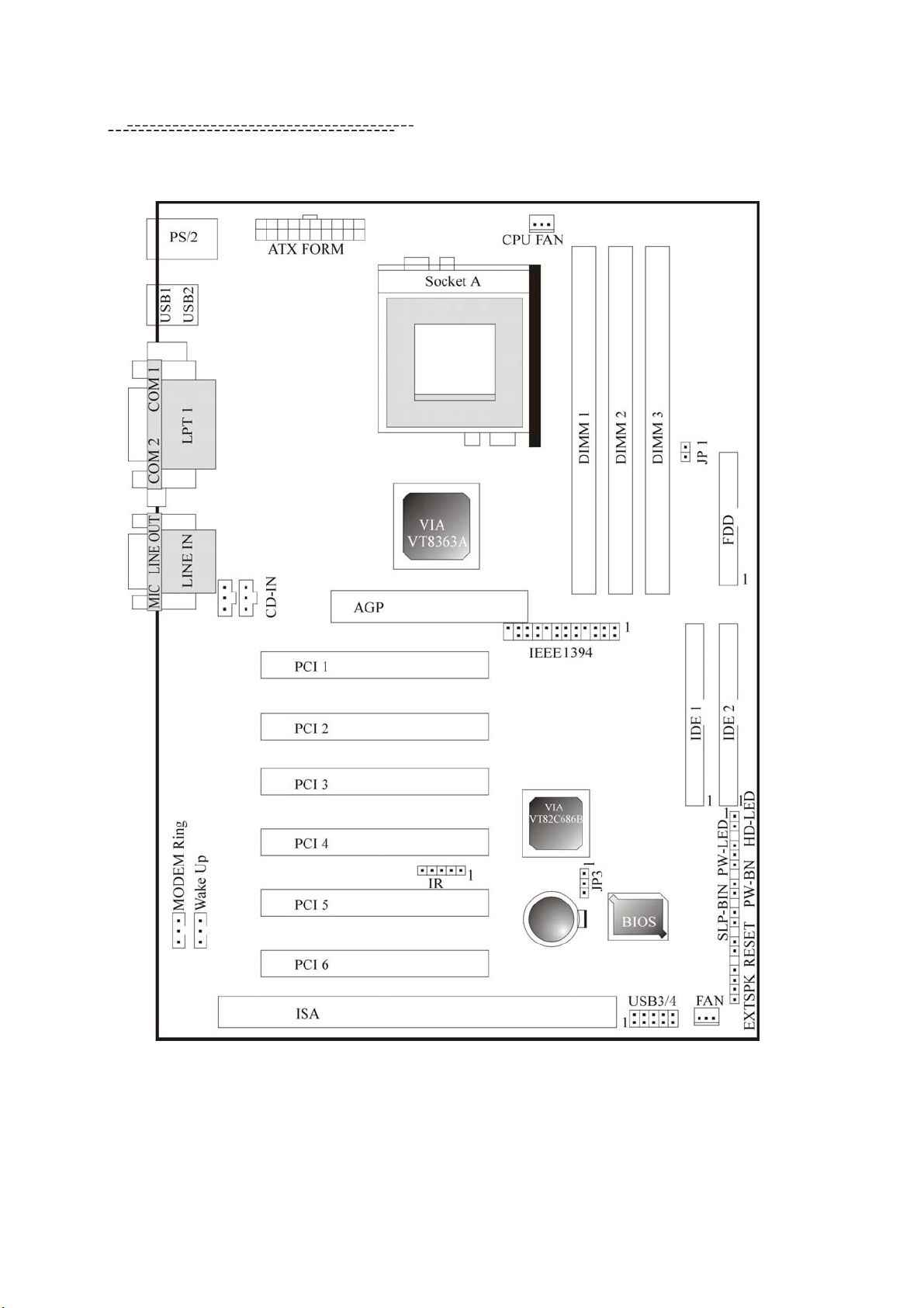
AGP PM-V06 User manual


V06
Copyright
Copyright2000 by this company. All rights reserved.
No part of this publication may be reproduced, transmitted, transcribed, stored in a retrieval
system, or translated into any language in any form or by any means, electronic, mechanical,
magnetic, optical, manual or otherwise, without the prior written consent of the copyright holders.
User’s Notice
The contents of this publication are subject to change. This company reserves the right to
alter the contents of this publication at any time and without notice. The contents of this
publication may contain inaccuracies or typographical errors and are supply for informational
use only.
Trademarks
All trademarks used in this manual are the property of their respective owners.
Intel and Pentium are registered trademarks of Intel Corporation.
PS/2 and OS/2 are registered trademarks of IBM Corporation.
Windows 95 / 98 and Windows NT are registered trademarks of Microsoft Corporation.
Netware is a registered trademark of Novell.
AWARD is a registered trademark of Award Software Inc.
AMD is a registered trademark of AMD.
Cyrix is a registered trademark of Cyrix.

V06
FCC Compliance
Federal Communications Commission Statement
This device complies with FCC Rules Part 15. Operation is subject to the following two
conditions:
• This device may not cause harmful interference, and
• This device must accept any interference received, including interference that may cause
undesired operation.
This equipment has been tested and found to comply with the limits for a Class B digital
device, pursuant to Part 15 of the FCC Rules. These limits are designed to provide reasonable
protection against harmful interference in a residential installation. This equipment generates,
uses and can radiate radio frequency energy and, if not installed and used in accordance with the
manufacturer’s instructions, may cause harmful interference to radio communication. However,
there is no guarantee that interference will not occur in a particular installation. If this equipment
does cause harmful interference to radio or television reception, which can be determined by
turning the equipment off and on, the user is encouraged to try to correct the interference by one
or more of the following measures:
• Re-orient or relocate the receiving antenna.
• Increase the separation between the equipment and the receiver.
• Connect the equipment to an outlet on a circuit different from that to which the receiver is
connected.
• Consult the dealer or an experienced radio/TV technician for help.
Warning!
The use of shielded cables for the connection of the monitor to the graphics card
is required to assure compliance with FCC regulations Changes or modifications
to this authority to operate this equipment.

V06
Table of Contents
Chapter 1 Introduction
1-1 Summary P1
1-2 Packing Check List P1
1-3 Mainboard Specification P 2
1-4 Mainboard Layout P4
Chapter 2 Hardware Installation
2-1 CPU P7
2-2 Panel Connector P11
2-3 Power Supply Connector P14
2-4 Hard Disk and Floppy Drive Connector: IDE 1 IDE 2 and FDD P15
2-5 IrDA Infrared Module Connector P16
2-6 Serial devices (COM1/COM2) , Parellel devices (LPT1) P17
2-7 PS / Keyboard , Mouse Connector P18
2-8 USB devices connector P19
2-9 IEEE1394 Connector P20
2-10 Audio / Game Connector P21
2-11 LAN Wake up / Modem Wake up P22
Chapter 3 BIOS Setup
3-1 Entering BIOS Setup P24
3-2 Getting Help P25
3-3 Main Menu P26
3-4 Setup Items P26

V06
3-5 Standard COMS Setup P28
3-6 Main Menu Selections P28
3-7 Advanced BIOS Features P29
3-8 Advanced Chipset Features P34
3-9 DRAM Settings P35
3-10 Integrated Peripherals P38
3-11 Power Management P42
3-12 PnP / PCI Configuration Setup P44
3-13 PC Health Status P46
3-14 Frequency / Voltage Control P46
3-15 Defaults Menu P47
3-16 Supervisor / User Password Setting P48
3-17 Exiting Selecting P49
Chapter 4 Driver Installation
4-1 Driver Installation for Windows95 / 98 P50
4-2 Driver Installation for Windows2000 P53

Chapter 1
Introduction
1-1 Summary
Thanks for purchasing this PM-V06 series mainboard, which is a high-performance computer
mainboard based on the VIA KT133(E) /KT 133A chipset. There are two designs of this series: PM-V06A
and PM-V06G.
KT133/KT133(E) is adopted in PM-V06G to support 200MHz system front side bus, while KT133A
chipset is used in PM-V06A, which support 266Mhz and PowerNow. PM-V06 series mainboard is designed
for new Althon and Dulon processor. The VIA VT82C686B south bridge chipset also provides full support of
Ultra DMA 33/66/100, delivering quick & reliable data transmission and conversion.
1-2 Packing Check List
This mainboard package contains the following items:
A VIA KT133(E)/KT133A series chipset ATX Mainboard
A UDMA 100 Data Cable
A Floppy Interface Cable
A piece of Driver CD
A USB connector cable
A COM2 (serial port) connector cable
An IEEE1394 connector cable
A User’s Manual

V06
1-3 Mainboard Specification
Form Factor ATX
Board Size 30.5 cm x 21.3cm
C P U
KT133 E/KT133A
PM-V06A KT133A
VIA VT8363A+VT82C696B
PM-V06G KT133/E
VIA VT8363 E+VT82C686B
Support AMD Duron series Athlon series and Socket A
processor
Support CPU host clock 550MHz-1GHz or higher
Support CPU Clock Ratio 3.5- 9 times or higher limited
by CPU
Support CPU clock frequency PM-V06A 200-
266Mhz(over clock to 332 Mhz)
PM-V06G -----200MHz over clock to 266MHz
Jumperless Overclock
Support CPU type/clock by BIOS setup
Support linear adjustment of CPU Clock Frequency:
Frequency over clock (non-recommended)
System Memory
DIMM 168pin x 3, maximum capability 1.5GB
Support 16M bit/64M bit/128M bit/256M bit /512M SDRAM
Refresh Mechanism:CBR supported only
Enhance Open page Arbitration SDRAM paging scheme
Audio
AC’97 ALC200 audio chipset
Provides LINE –OUT, LINE-IN and Microphone connector
Provides CD-IN connector
Expansion Slots
1 x AGP bus slot (AGP 4X)
6 x PCI slot
1 x ISA slot

V06
Serial Port
Two serial ports UART 16C550 Compatible
Sets serial port 2 to operate in normal mode, IrDA
Parallel Port
A parallel port support:
SPP-Standard parallel port
EPP-enhanced parallel port
ECP-extended capabilities port
Floppy Interface
Support drivers inches/ format with
3.5 inches -720KB/1.44MB/2.88MB
5.25 inches -360KB/1.2MB
I D E Interface
Dual PCI IDE interface support up to 4 x EIDE/ IDE devices
Support PIO mode4, DIMA mode 2 and Ultra DMA33/66/100
mode
U S B Interface
Two USB ports supported
Two additional USB ports, connected to the ports by cable
(optional)
USB legacy keyboard/mouse function supported
Support up to 127 USB devices
P S / 2 mouse PS/2 mouse port supported by connector onboard
Keyboard PS/2 keyboard supported by connector onboard
Battery Lithium (CR-2032) battery
Wake up Function
Modem ring wake up
LAN wake up
Keyboard wake up
Supports Wake –up from Sleeping State S1-S4
Synchronous
Switching
Register
High efficient synchronous switching regulator to CPU core
voltage from 1.3V to 2.05V
Supports over-voltage /over current protection function
Hardware Monitor
3 fans (CPU fan, Housing fan, Auxiliary fan) monitoring
Monitor 9 kinds of system voltage (5V_Dual, 12V, 5V, 1.5V,
3.3V, VCORE, -12V, -5V, battery), Detects VCORE from
VID0-4
Power Connector Supports ATX (20-pin) power connector
B I O S
2M bit Award BIOS
SM BIOS 2.3
Year 2000Compliance

V06
PCI 2.2 Compliance
PnP BIOS V1.0
APM V1.2 Compliance
DMI 2.0 Compliance
Flash Upgrade BIOS write protection
Support ACPI(Advance Configuration and Power Interface)
and OS direct Power Management
Support SOFT power off
Floppy drive detection function supported
Bus speed selected by BIOS
Integrated hardware Random Number Generator(RNG)
Register based locking
Hardware-based locking
L E D Indicator
System power LED
HDD activity LED
System Suspend LED (programming LED blinking to S1-S4
mode)
1-4 Mainboard Layout

V06
V06A Mainboard Layout

V06
V06G Mainboard Layout

V06
Chapter 2
Hardware Installation
This section gives you a step-by-step procedure on how to install your
system. Follow each section accordingly.
2-1 CPU
2-1.1 CPU Installation Procedures
The mainboard uses a CPU socket called Socket 370 for easy installation, please
follow the below figure to install the CPU.
2-1.2 CPU Clock Ratio Setting
System Frequency= CPU Clock Ratio CPU Clock Frequency
The mainboard support jumperless CPU type setting, no jumper or switch is needed.
This mainboard also support CPU over-clock by adjusting the CPU Clock Frequency and
CPU Clock Ratio under BIOS Setup.
The available settings are:
-CPU Clock Frequency
66 –166 linear step1MHz over clock
-CPU Clock Ratio
For AMD series CPU, due to the clock ratio is locked at present, the clock ratio is
Control Lever
Pin-1Cut ed
g
e
Pin-1Cut edge

V06
auto-detected and cognized by the mainboard.
Clock Frequency:
The mainboard supports CPU Host Clock over speed. Disable JP1 , the jumper will run CPU
at standard 1 clock frequency 200 / 266MHz( Default)
When JP1 enabled, CPU will be forced to run at clock frequency 266 / 332 MHz.
Warning:
At this moment, AMD Dulon and Authlon series CPU
normally support 200 / 266MHz Clock Frequency Besides
normal CPU clock frequency recommended the other
CPU clock frequency such as 266-330MHz are available
only for internal test or end-user over-clocking testing
which may cause your system unstable or error damage.
JP 1

V06
2-1.3 Memory Installation
System Memory Installation Procedures
1The DIMM slot has 2 notch keys, so the DIMM memory module can only fit in one
direction.
2Insert the DIMM memory bank vertically into DIMM slot, then press it down placidly and
uniformly.
3The plastic clip at the side of the DIMM will automatically close.
There are 2 pcs 168 pin DIMM sockets on the mainboard which support Synchronous
DRAM and Registered SDRAM, and it allows you to install system maximum up to 1024MB.
2-1.4 Type
The mainbaord supports 168PIN Synchronous DRAM and Registered SRAM. However,
mixing DRAM and Registered SDRAM is not allowed. Install one type only in your system for
better compatibility.
2-1.5 Speed
This motherboard supports PC-66 PC-100 or PC-133 memory only for high speed operation.
2-1.6 Buffered and non-buffered
Only the non-buffered DIMM can be used in this mainboard. The difference between
buffered and non-buffered DIMM can be identified by the notch position shown above.

V06
2-1.7 2-clock and 4-clock signal
2- clock and 4 -clock SDRAM DIMM is supported by this mainboard.
2-1.8 Parity and Non-parity
This mainboard supports standard 64 bit(Non-parity) and 72 bit (parity) DIMM modules.
2-1.9 Memory Auto-detected by BIOS
This mainboard BIOS can automatically detect the DIMM memory size and type, so you do
not need to adjust any hardware or software settings. The maximum memory size supported up to
512MB 2.
2-1.10 Recommended SDRAM combination
The mainboard support maximum up to 1.5GB 512M 3, it has three 168-pin
non-buffered DIMM (Double In-Line Memory Module) socket. The mainboard support the
following SDRAM combination.
DIMM Location DIMM Size Max. Memory Size
DIMM 1 SDRAM 8, 16, 32, 64 128, 256MB 512MB
DIMM 2 SDRAM 8, 16, 32, 64 128, 256MB 512MB
DIMM 3 SDRAM 8. 16, 32, 64, 128, 256MB 512MB
TotalSystemMemory 1.5GB
Warning
There are two kinds of DIMM specification supported by this
mainboard PC133 and PC100 . If you use 200MHz CPU,
PC100 & PC133 DIMM spec. is supported. If you use 266
MHz CPU, only PC133 DIMM spec. is supported.

V06
The memory speed normally pitch
-15 -12 -10 -7 -8 PC-100 PC-133
The meaning is:
-15=15ns, and the maximum clock is 66MHz
-12=12ns, and the maximum clock is 83MHz
-10=10ns, and the maximum clock is 100MHz
-8=7ns, and the maximum clock is 125MHz
-7=7ns, and the maximum clock is 142MHz
PC-100/PC133 = New Intel specification for high memory speed with
100/133MHz or above CPU Bus Clock.
This motherboard supports all the above memory speeds. For better system performance and
reliability issue, we suggest that you use PC-100 SDRAM or above CPU Bus Clock is used in
your system.
2-2 Panel Connector
EXTSPK RESET SLP-BIN PW-BN PW-LED HD-LED

V06
Speaker EXTSPK
Speaker from the system case is connected to this pin.
Pin Description
1 Data out
2 N.C.
3 Ground
4 +5V
RESET Switch: RESET
RESET switch is used to reboot the system rather than turning the power On/Off. Do not
reboot the system when the HDD LED is flickering, you can connect the RESET switch from the
system case on this pin.
Setting Description
Open Normal Mode
Close Reset system
Sleeping Switch: SLP-BIN
When you short this switch, the system will be in sleep.
ATX Soft-power Switch Connector: PW-BIN
Connect to a 2-pin push power button switch from Computer case, .it provides instant On/Off
function
Keylock and Power LED Connector: PW-LED
Keylock allows you to disable the keyboard for security purpose. You can connect the
keyboard to this pin, or you can connect the PW-LED cable to the 1-3 pin.
Pin Description
1 LED output
2 N.C.
3 Ground
4 Keylock
5 Ground

V06
HDD LED Connector: HD-LED
HDD LED shows the activity of a hard disk drive. Avoid turning the power off while the
HDD led is twinkling. You can connect HDD LED from the system case to this pin.
2-2.1 CMOS Clear Setting
CMOS Jumper
Please refer the following figures for the locations of the jumper on the mainboard.
JP3
To clear CMOS, please follow the steps below:
1. Power off the system and unplug the chassis AC power cord.
2. Short JP7 at pin2-3 for 10-15 seconds.
3. Set JP7 back to its Normal position at pin1-2.
4. Plug the AC power cord to the chassis.
5. Power on the system and load the BIOS setup defaults.
Pin Description
1 Active Signal
2 Ground
3 Ground
4 Active Signal
1
CLEAR COMS KEEP DATA

V06
Note:
You can clear CMOS by shorting 2-3 pin for 10-15 seconds,
while the system is off. Then, return to 1-2 in position, Avoid
clearing the CMOS while the system is on, it will damage the
mainboard.
2-3 Power Supply Connector
Connect the power supply cable to the power connector. Using the ATX power supply
functions such as wake-Up Modem is supported by this mainboard.
ATXFORM
Warning:
Since the mainboard has the instant power on function, make
sure that all components are installed properly before
inserting the power connector to ensure that no damage will
be done.

V06
The ATX power supply provides a single 20-pin connector.
Pin Description Pin Description
1
2
3
4
5
6
7
8
9
10
3.3V
3.3V
Ground
+5V
Ground
+5V
Ground
Power OK
5VSB
+12V
11
12
13
14
15
16
17
18
19
20
3.3V
-12V
Ground
PS-ON
Ground
Ground
Ground
-5V
+5V
+5V
Note:
Some ATX–power does not have –5V voltage output, it will
effect some function of ADD-ON card devices.
2-4 Hard Disk and Floppy Drive Connector: IDE1 IDE2 and FDD
The mainboard has a 32-bit Enhanced IDE controller that provides PIO mode 0-4, Bus
Master, and Ultra DMA33/66 function. It has two HDD connectors IDE1 (primary) and IDE2
(secondary). You can connect up to four hard disk drives, CD-ROM and other devices to IDE1
and IDE2.
Moreover, to each group of IDE connector, IDE can connect a Master and a Slave driver.
IDE1 Primary IDE Connector marked with blue
The first hard drive should always be connected to IDE1. IDE1 can connected a Master and a
slave drive. You must configure second hard drive to slave mode by setting the jumper
accordingly.
IDE2 Secondary IDE Connector
IDE2 can also connect a Master and a Slave drive.
Table of contents
Other AGP Motherboard manuals