Alpha Data ADM-PCIE-9V3 User manual

ADM-PCIE-9V3
User Manual
Document Revision: 2.7
4th December 20 8

ADM-PCIE-9V3 User Manual
© 20 8 Copyright Alpha Data Parallel Systems Ltd.
All rights reserved.
This publication is protected by Copyright Law, with all rights reserved. No part of this
publication may be reproduced, in any shape or form, without prior written consent from Alpha
Data Parallel Systems Ltd.
Head Office
Address: 4 West Silvermills Lane
Edinburgh, EH3 5B , UK
Telephone: +44 131 558 2600
Fax: +44 131 558 2700
email: [email protected]
website: http://www.alpha-data.com
US Office
611 Corporate Circle, Suite H
Golden, CO 80401
(303) 954 8768
(866) 820 9956 - toll free
http://www.alpha-data.com
All trademarks are the property of their respective owners.

ADM-PCIE-9V3 User Manual
Table Of Contents
Introduction ......................................................................................................................................
1.1 Key Features ................................................................................................................................. 1
1.2 Order Code .................................................................................................................................... 1
2 PCB Information .............................................................................................................................. 2
2.1 Physical Specifications .................................................................................................................. 2
2.2 Chassis Requirements ................................................................................................................... 2
2.2.1 PCI E press ............................................................................................................................... 2
2.2.2 Mechanical Requirements ......................................................................................................... 2
2.2.3 Power Requirements ................................................................................................................. 2
2.3 Thermal Performance .................................................................................................................... 3
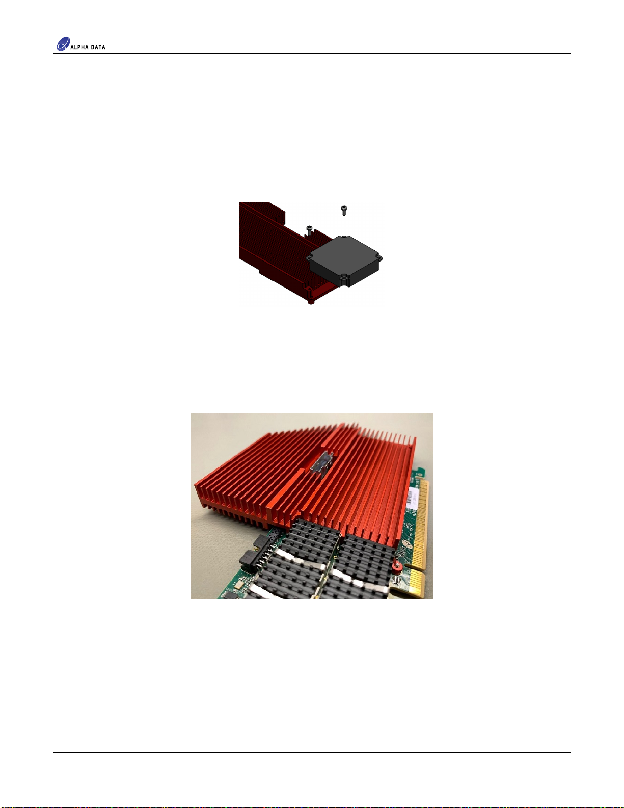
2.4 Optional Blower ............................................................................................................................. 4
2.5 Full Height Heat Sink ..................................................................................................................... 4
3 Functional Description .................................................................................................................... 5
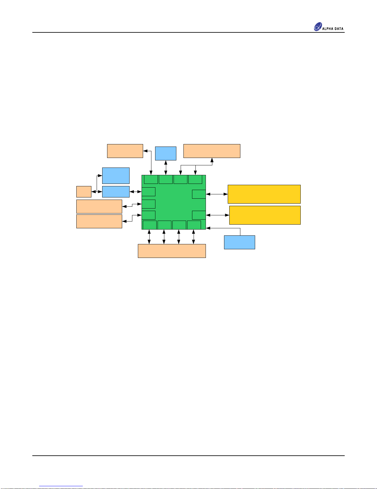
3.1 Overview ........................................................................................................................................ 5
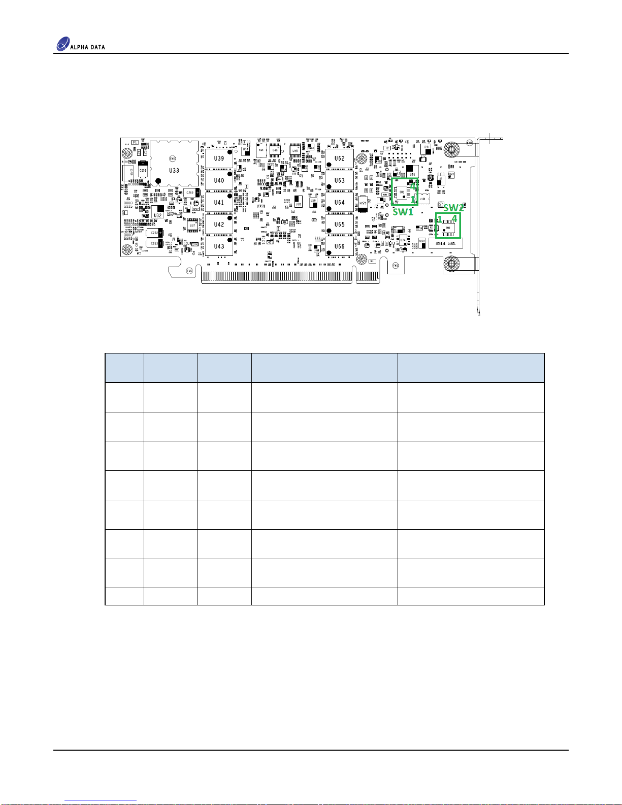
3.1.1 Switches .................................................................................................................................... 6
3.1.2 LEDs .......................................................................................................................................... 7
3.2 Clocking ......................................................................................................................................... 8
3.2.1 PCIe Reference Clocks ............................................................................................................. 8
3.2.2 Fabric Clock ............................................................................................................................... 8
3.2.3 Programming Clock (EMCCLK) ................................................................................................. 9
3.2.4 QSFP28 ..................................................................................................................................... 9
3.2.5 Ultraport SlimSAS .................................................................................................................... 10
3.2.6 DDR4 SDRAM Reference Clocks ............................................................................................ 10
3.3 PCI E press ................................................................................................................................. 11
3.4 DDR4 SDRAM ............................................................................................................................. 11
3.5 QSFP28 ....................................................................................................................................... 12
3.6 OpenCAPI Ultraport SlimSAS ...................................................................................................... 13
3.7 System Monitor ............................................................................................................................ 14
3.7.1 System Monitor Status LEDs ................................................................................................... 15
3.8 USB Interface .............................................................................................................................. 16
3.9 Configuration ............................................................................................................................... 16
3.9.1 Configuration From Flash Memory .......................................................................................... 16
3.9.1.1 Building and Programming Configuration Images ............................................................... 17
3.9.2 Configuration via JTAG ............................................................................................................ 17
3.10 GPIO Connector .......................................................................................................................... 18
3.10.1 Direct Connect FPGA Signals .................................................................................................. 18
3.10.2 Timing Input ............................................................................................................................. 18
3.11 User EEPROM ............................................................................................................................. 19
Appendix A Complete Pinout Table .................................................................................................................. 2
List of Tables
Table 1 Mechanical imensions ..................................................................................................................... 2
Table 2 Available Power By Rail ..................................................................................................................... 2
Table 3 Switch Functions ................................................................................................................................ 6
Table 4 LE etails ........................................................................................................................................ 7
Table 5 PCIe Reference Clocks ..................................................................................................................... 8
Table 6 Fabric Clock ....................................................................................................................................... 9
Table 7 EMCCLK ............................................................................................................................................ 9

ADM-PCIE-9V3 User Manual
Table 8 QSFP28 Reference Clocks ................................................................................................................ 9
Table 9 QSFP28 Jitter Attenuated Reference Clocks ..................................................................................... 9
Table 10 SlimSAS Reference Clocks (OpenCAPI) ......................................................................................... 10
Table 11 Memory Reference Clocks .............................................................................................................. 10
Table 12 QSFP28 Part Numbers .................................................................................................................... 12
Table 13 Voltage, Current, and Temperature Monitors ................................................................................... 14
Table 14 Status LE efinitions ..................................................................................................................... 15
Table 15 Complete Pinout Table ..................................................................................................................... 21
List of Figures
Figure 1 A M-PCIE-9V3 Product Photo .......................................................................................................... 1
Figure 2 Thermal Performance ........................................................................................................................ 3
Figure 3 Optional Blower ................................................................................................................................. 4
Figure 4 Full Height Heat Sink ......................................................................................................................... 4
Figure 5 A M-PCIE-9V3 Block iagram ......................................................................................................... 5
Figure 6 Switches ............................................................................................................................................ 6
Figure 7 Backside LE s .................................................................................................................................. 7
Figure 8 Front Panel LE s .............................................................................................................................. 7
Figure 9 Clock Topology .................................................................................................................................. 8
Figure 10 Si5328 Block iagram ..................................................................................................................... 10
Figure 11 QSFP Locations ............................................................................................................................... 12
Figure 12 OpenCAPI Location ......................................................................................................................... 13
Figure 13 Flash Address Map .......................................................................................................................... 16
Figure 14 GPIO Connector Schematic ............................................................................................................ 18
Figure 15 GPIO Connector Location ................................................................................................................ 18

ADM-PCIE-9V3 User Manual
Introduction
The A M-PCIE-9V3 is a high-performance reconfigurable computing card intended for ata Center applications,
featuring a Xilinx Virtex UltraScale Plus FPGA.
Figure : ADM-PCIE-9V3 Product Photo
. Key Features
Key Features
• PCIe Gen1/2/3 x1/2/4/8/16 capable
• Half-length, low-profile x16 PCIe form factor
• Two banks of R4 S RAM 72 bit wide memory (ECC), 16GB (8GB per bank) default rated at 2400MT/s,
32GB option rated at 1866MT/s.
• Two QSFP28/zQSFP+ sites capable of data rates up to 28 Gbps per channel (112 Gbps per cage)
• One 8 lane Ultraport SlimSAS connector that is compliant with OpenCAPI
• Optional timing input
• Front panel and rear edge JTAG access via USB port
• FPGA configurable over USB/JTAG and SPI configuration flash
• XCVU3P-2FFVC1517I FPGA
• Voltage, current, and temperature monitoring
.2 Order Code
A M-PCIE-9V3
See http://www.alpha-data.com/pdfs/adm-pcie-9v3.pdf for complete ordering options.
Page Introduction
ad-ug- 322_v2_7.pdf

ADM-PCIE-9V3 User Manual
2 PCB Information
2. Physical Specifications
The A M-PCIE-9V3 complies with PCI Express CEM revision 3.0.
escription Measure
Total y 68.9 mm
Total x (Inc. QSFP Cages) 174 mm
Total z 17.45 mm
Weight 230 grams
Table : Mechanical Dimensions
2.2 Chassis Requirements
2.2. PCI Express
The A M-PCIE-9V3 is capable of PCIe Gen 1/2/3 with 1/2/4/8/16 lanes, using the Xilinx Integrated Block for PCI
Express.
2.2.2 Mechanical Requirements
A 16-lane physical PCIe slot is required for mechanical compatibility.
Each A M-PCIE-9V3 is shipped with a full height PCIe card bracket installed by default. A half-height bracket is
shipped along with the product and can be easily changed out with a Philips screw driver. If the application
requires a low-profile bracket and the order quantity is high, contact [email protected] to get the correct
bracket fitted before shipping.
2.2.3 Power Requirements
The PCIe Specification permits a standard low-profile, half-length PCIe card to dissipate up to 25 W of power,
drawn from the PCIe slot. The A M-PCIE-9V3 may consume more than 25 W of power for larger user FPGA
designs. Power estimation requires the use of the Xilinx XPE spreadsheet and/or a power estimator tool
available from Alpha ata. Please contact [email protected] to obtain this tool.
The power available to the rails calculated using XPE are as follows:
Voltage Source Name Current Capability
0.85 VCC_INT + VCCINT_IO + VCC_BRAM 36A
1.8 VCCAUX + VCCAUX_IO + VCC_BRAM + VCCO_1.8V 6A
3.3 VCCO_3.3V 6A
1.2 VCCO_1.2V 9A
1.8 MGTVCCAUX 1A
0.9 MGTAVCC 9A
1.2 MGTAVTT 15A
Table 2 : Available Power By Rail
Page 2 PCB Information
ad-ug- 322_v2_7.pdf

ADM-PCIE-9V3 User Manual
2.3 Thermal Performance
If the FPGA core temperature exceeds 100 degrees Celsius, the FPGA design will be cleared to prevent that
card from over-heating.
The A M-PCIE-9V3 comes with a heat sink to reduce the heat of the FPGA which is typically the hottest point on
the card. The FPGA die temperature must remain under 100 degrees Celsius. To calculate the FPGA die
temperature, take your application power and multiply by Theta JA from the table below, and add to your system
internal ambient temperature. If you are using the fan provided with the board, you will find theta JA is
approximately 1.4 degC/W for the board in still air.
The power dissipation can be estimated by using the Alpha ata power estimator in conjunction with the Xilinx
Power Estimator (XPE) downloadable at http://www.xilinx.com/products/technology/power/xpe.html. ownload
the UltraScale tool and set the evice to Virtex UltraScale+, VU3P, FFVC1516, -2, Industrial. Set the ambient
temperature to your system ambient and select User Override for the Effective theta JA and enter the figure
associated with your system LFM in the blank field. Proceed to enter all applicable design elements and
utilization in the following spreadsheet tabs. Next aquire the 9V3 power estimator from Alpha ata by contacting
[email protected]. You will then plug in the FPGA power figures along with R4 and QSFP usage to get
an estimate.
Figure 2 : Thermal Performance
Page 3PCB Information
ad-ug- 322_v2_7.pdf

ADM-PCIE-9V3 User Manual
2.4 Optional Blower
Because it is possible for generic PC chassis to not provide sufficient airflow to cool the FPGA, the
A M-PCIE-9V3 is shipped with an uninstalled blower. The blower is optional and can be easily installed with a
Philips screw driver at the discretion of the user. Ensure the opening is facing the heatsink fins. The blower
hangs off the back of the PCB outside of the PCIe card envelope. After screwing the blower into the heatsink,
plug in the small power connector into the connector in the corner of the board. It is possible to alternatively ship
a fan that fits in the adjacent PCIe card slot if required for mechanical fit, contact [email protected] for
details.
Figure 3 : Optional Blower
2.5 Full Height Heat Sink
For customers with full height chassis that would like better thermal performance, and to baffle the empty space
above the card, Alpha ata sells a full height heat sink variant. The thermal performance boost is documented in
the Thermal Performance image above. Contact [email protected] for more details.
Figure 4 : Full Height Heat Sink
Page 4 PCB Information
ad-ug- 322_v2_7.pdf

ADM-PCIE-9V3 User Manual
3 Functional Description
3. Overview
The A M-PCIE-9V3 is a versatile reconfigurable computing platform with a Virtex UltraScale VU3P FPGA, a
Gen3x16 PCIe interface, two banks of R4 both 72 bits wide (for 64 bits with 8 bits ECC), two QSFP28 cages
capable of 8x 28G or 2x 112G Serial IO of any Xilinx supported standard (Ethernet, SRIO, Infiniband, etc.), one
OpenCAPI compatible Ultraport SlimSAS connector also capable of 28G/channel, an input for a timing
synchronization input, a 12 pin header for general purpose use (clocking, control pins, debug, etc.), and a robust
system monitor.
XCVU3P-2
FFVC1517I
(0,4) (5,7) (8,11) (12,15)
x16 PCIe Gen3/4 Edge
QSFP28 C ge
(4x28 Gbps m x)
QSFP28 C ge
(4x28 Gbps m x) DDR4 B nk 1
DDR4-2400/1866, 8/16GB
DDR4 B nk 0
DDR4-2400/1866, 8/16GB
System
Monitor
MGT
MGT HPIO
HPIO
HRIO
x8 SPI
Config
x72
x72
MGTMGT MGT
HRIO
USB JTAG 0
Auxili ry IO
(gpio, timing)
MGTMGT
OpenCAPI SAS
(8x28Gbps m x)
MGT
MAC ID
EEPROM
Figure 5 : ADM-PCIE-9V3 Block Diagram
Page 5Functional Description
ad-ug- 322_v2_7.pdf

ADM-PCIE-9V3 User Manual
3. . Switches
The A M-PCIE-9V3 has a quad IP switch SW1, located on the rear side of the board. The function of each
switch in SW1 is detailed below:
Figure 6 : Switches
Switch Factory
efault Function OFF State ON State
SW1-1 OFF User
Switch 0 Pin AV27 = '1' Pin AV27 = '0'
SW1-2 OFF User
Switch 1 Pin AW27 = '1' Pin AW27 = '0'
SW1-3 OFF Service
Mode Regular Operation Firmware update service mode
SW1-4 OFF JTAG
Source JTAG to FPGA from USB JTAG to FPGA from debug
header
SW2-1 ON HOST_I2
C_EN Sysmon over PCIe I2C Sysmon isolated
SW2-2 ON CAPI_VP
_EN OpenCAPI VP available OpenCAPI VP isolated
SW2-3 ON CAPI_VP
_WP CAPI VP is write protected CAPI VP is writable
SW2-4 ON Reserved Reserved Reserved
Table 3 : Switch Functions
Use IO Standard "LVCMOS18" when constraining the user switch pin.
Page 6 Functional Description
ad-ug- 322_v2_7.pdf

ADM-PCIE-9V3 User Manual
3. .2 LEDs
There are 8 LE s on the A M-PCIE-9V3, 5 of which are general purpose and whose meaning can be defined by
the user. The other 3 have fixed functions described below:
USR_LED_G0
D2 D4 D7 D8
USER_LED_G1 USR_LED_R
DONE
Figure 7 : Backside LEDs
Front_LED_0
D5 D6 D9
Front_LED_1STAT_0 STAT_1
D10
Figure 8 : Front Panel LEDs
Comp.
Ref. Function ON State OFF State
4 ONE FPGA is configured FPGA is not configured
8
USER_LE _G0
User defined '0' pin AT27 User defined '1' pin AT27
2
USER_LE _G1
User defined '0' pin AU27 User defined '1' pin AU27
7 USER_LE _R User defined '0' pin AU23 User defined '1' pin AU23
5 Status 0 See Status LE efinitions
6 Status 1 See Status LE efinitions
9 Front_LE _0 User defined '1' pin AH24 User defined '0' pin AH24
10 Front_LE _1 User defined '1' pin AJ23 User defined '0' pin AJ23
Table 4 : LED Details
Use IO Standard "LVCMOS18" when driving the user LE pins.
Page 7Functional Description
ad-ug- 322_v2_7.pdf

ADM-PCIE-9V3 User Manual
3.2 Clocking
The A M-PCIE-9V3 provides reference clocks for the R4 S RAM banks and the I/O interfaces available to
the user. After a clock is programmed to a certain frequency, that frequency will become the default on power-up.
Any clock out of an Si5338 Clock Synthesizer is re-configurable from either the front panel USB USB Interface or
the Alpha ata bridge IP available in the board support package (sold separately). This allows the user to
configure almost any arbitrary clock frequencies during application run time. Maximum clock frequency is
312.5MHz.
Note: use "set_property BITSTREAM.CONFIG.UNUSE PIN {Pullnone} [current_design]" to ensure the user
design does not interfere with the I2C interface to the reprogramable clock generator.
NB6L11S
Fanout QSFP28 161.1328125MHz Factory Default (M TREFCLK0_128)
QSFP28 161.1328125MHz Factory Default (M TREFCLK0_127)
FABRIC_CLK 300MHz (IO Bank 64)
Card Edge PCIe Ref Clock (100MHz)
25MHz
30ppm
Source
Si5338
Clock
Synth
NB6L11S
Fanout CAPI 161.1328125MHz Factory Default (M TREFCLK0_125)
CAPI 161.1328125MHz Factory Default (M TREFCLK0_124)
NB6L11S
Fanout
Memory Interface Clock 300Mhz (IO Bank 44)
Memory Interface Clock 300Mhz (IO Bank 64)
NB6L11S
Fanout PCIe Ref Clock (M TREFCLK0_224)
PCIe Ref Clock (M TREFCLK0_226)
CAPI Cable Clock (156.25MHz when used) NB6L11S
Fanout CAPI Cable Clock (M TREFCLK1_125)
CAPI Cable Clock (M TREFCLK1_124)
Figure 9 : Clock Topology
3.2. PCIe Reference Clocks
The 16 MGT lanes connected to the PCIe card edge use MGT quads 224 through 227 and use the system 100
MHz clock (PCIE_REFCLK).
Signal Target FPGA Input I/O Standard "P" pin "N" pin
PCIE_REFCLK1 MGTREFCLK0_226 HCSL AA7 AA6
PCIE_REFCLK2 MGTREFCLK0_224 HCSL AJ7 AJ6
Table 5 : PCIe Reference Clocks
3.2.2 Fabric Clock
The design offers a fabric clock called FABRIC_CLK which is permanently fixed at 300 MHz. This clock is
intended to be used for I ELAY elements in FPGA designs. The fabric clock is connected to a Global Clock (GC)
pin.
Page 8 Functional Description
ad-ug- 322_v2_7.pdf

ADM-PCIE-9V3 User Manual
Signal Target FPGA Input I/O Standard "P" pin "N" pin
FABRIC_CLK IO_L12P_T1U_GC_64 LV S AP26 AP27
Table 6 : Fabric Clock
IFF_TERM_A V = TERM_100 is required for LV S termination
3.2.3 Programming Clock (EMCCLK)
An 100MHz clock is fed into the EMCCLK pin to drive the SPI flash device during configuration of the FPGA.
Note that this is not a global clock capable IO pin.
Signal Target FPGA Input I/O Standard pin
REFCLK100M IO_L24P_T3U_N10_EMCCLK_65 LVCMOS18 AJ28
Table 7 : EMCCLK
3.2.4 QSFP28
The QSFP28 cages are located in MGT quads 127 and 128 and use a 161.1328125MHz default reference clock.
Note that this clock frequency can be changed to any arbitrary clock frequency up to 312MHz by re-programing
the Si5338 reprogrammable clock oscillator via system monitor. This can be done using the Alpha ata API or
over USB with the appropriate Alpha ata Software tools.
Signal Target FPGA Input I/O Standard "P" pin "N" pin
GTY_CLK_0B MGTREFCLK0_128 LV S N33 N34
GTY_CLK_0C MGTREFCLK0_127 LV S U33 U34
Table 8 : QSFP28 Reference Clocks
The QSFP28 cages are also located such that they can be clocked from a Si5328 jitter attenuator clock
multiplier. If jitter attenuation is required please see the reference documentation for the Si5328. https://
www.silabs.com/Support%20 ocuments/Technical ocs/Si5328.pdf
The Si5328 is configured with a 114.285MHz oscilator on XA and XB
The Si5328 S A pin connects at FPGA pin L29 (1.8V), SCL is at FPGA pin L30 (1.8V) with external pull-ups
included.
The Si5328 can be reached at I2C address 1101000
The Si5328 input clock comes from FPGA pins M29 and M30, and includes 100 Ohm differential termination and
100nF AC coupled termination from the 1.8V FPGA bank suitable for LV S signal levels.
The Si5328 output clocks are AC coupled with 10nF capacitors and then connected to the FPGA MGTREFCLK
pins shown in the table below. LV S signal standard is recommended on these nets as well.
Signal Target FPGA Input I/O Standard "P" pin "N" pin
SI5328_REFCLK_OUT0
MGTREFCLK1_128 LV S L33 L34
SI5328_REFCLK_OUT1
MGTREFCLK1_127 LV S R33 R34
Table 9 : QSFP28 Jitter Attenuated Reference Clocks
Page 9Functional Description
ad-ug- 322_v2_7.pdf

ADM-PCIE-9V3 User Manual
FPGA
Si5328
(2.5V VCC)
A0 = A1 = A2= GND
CS_CA = CMODE = GND
Other co trol pi s = N/C
GPIO (LVCMOS18)
SI5328_1V8_SDA
SI5328_1V8_SCL
I2C
CLKOUT2
CLKOUT1
Crystal
114.285MHz XA/XB
CLKIN1
GPIO (LVDS)
SI5328_REFCLK_IN_P
SI5328_REFCLK_IN_N
MGT REFCLK (LVDS)
SI5328_REFCLK_OUT0_P
SI5328_REFCLK_OUT0_N
MGT REFCLK (LVDS)
SI5328_REFCLK_OUT1_P
SI5328_REFCLK_OUT1_N
Figure 0 : Si5328 Block Diagram
3.2.5 Ultraport SlimSAS
The Ultraport SlimSAS connector is located in MGT quads 124 and 125 and use a 161.1328125MHz default
reference clock. Note that this clock frequency can be changed to any arbitrary clock frequency up to 312MHz by
re-programing the Si5338 reprogrammable clock oscillator via system monitor. This can be done using the Alpha
ata API or over USB with the appropriate Alpha ata Software tools.
Signal Target FPGA Input I/O Standard "P" pin "N" pin
GTY_CLK_1B MGTREFCLK0_125 HCSL AE33 AE34
GTY_CLK_1C MGTREFCLK0_124 HCSL AJ33 AJ34
CAPI_CLK_C MGTREFCLK1_125 HCSL AC33 AC34
CAPI_CLK_ MGTREFCLK1_124 HCSL AG33 AG34
Table 0 : SlimSAS Reference Clocks (OpenCAPI)
3.2.6 DDR4 SDRAM Reference Clocks
The two banks of R4 S RAM memory each require a separate reference clock, as per Xilinx UltraScale MIG
design guidelines. The reference clocks for these interfaces are detailed below:
Both clocks are 300MHz by default.
Signal Target FPGA Input I/O Standard "P" pin "N" pin
MEM_CLK_0 IO_L13_T2L_GC_44 LV S G31 G32
MEM_CLK_1 IO_L11_T2L_GC_64 LV S AN25 AN26
Table : Memory Reference Clocks
IFF_TERM_A V = TERM_100 is required for LV S termination
Page 0 Functional Description
ad-ug- 322_v2_7.pdf

ADM-PCIE-9V3 User Manual
3.3 PCI Express
The A M-PCIE-9V3 is capable of PCIe Gen 1/2/3 with 1/2/4/8/16 lanes. The FPGA drives these lanes directly
using the Integrated PCI Express block from Xilinx. Negotiation of PCIe link speed and number of lanes used is
generally automatic and does not require user intervention.
PCI Express reset (PERST#) connected to the FPGA at two locations. See Complete Pinout Table signals
PERST_1V8_0 and PERST_1V8_1.
The other pin assignments for the high speed lanes are provided in the pinout attached to the Complete Pinout
Table
The PCI Express specification requires that all add-in cards be ready for enumeration within 120ms after power
is valid (100ms after power is valid + 20ms after PERST is released). The A M-PCIE-9V3 does meet this
requirement when configured from a tandem bitstream with the proper SPI constraints detailed in the section:
Configuration From Flash Memory. For more details on tandem configuration, see Xilinx xapp 1179.
Note:
ifferent motherboards/backplanes will benefit from different RX equalization schemes within the PCIe IP core
provided by Xilinx. Alpha ata recommends using the following setting if a user experiences link errors or
training issues with their system: within the IP core generator, change the mode to "Advanced" and open the
"GT Settings" tab, change the "form factor driven insertion loss adjustment" from "Add-in Card" to
"Chip-to-Chip" (See Xilinx PG239 for more details).
3.4 DDR4 SDRAM
Two banks of R4 S RAM memory are soldered down to the board. While the factory default is 8GB/per bank,
16GB/bank is also supported through a built variant. Please see Order Code for all order options. The memory
interface is 72-bit wide data (64 data + 8 ECC). Maximum signaling rate is 2400 MT/s for 16GB total and
2133MT/s with 32GB total.
Memory solutions are available from the Xilinx Memory Interface Generator (MIG) tool. An example memory
exerciser project is included in the A M-PCIE-9V3 S K. All constraint information is included in Complete Pinout
Table. Alpha ata has also provided a custom csv timing file for use with Xilinx MIG. This can be downloaded
from the A M-PCIE-9V3 product page.
8Gb components used (standard) are Samsung K4A8G085WB-BCRC
16Gb components used (build variant) are Micron MT40A2G8PM-093E
When using the timing files provided on the alpha data product page custom_parts_2400.csv , always use the
samsung timing files, as they are more relaxed than the micron variants.
Page Functional Description
ad-ug- 322_v2_7.pdf

ADM-PCIE-9V3 User Manual
3.5 QSFP28
Two QSFP28 cages are available at the front panel. Both cages are capable of housing either active optical or
passive copper QSFP28 or QSFP compatible components. The communication interface can run at up to
28Gbps per channel. There are eight channels between the two QSFP28 cages (total maximum bandwidth of
224Gbps). These cages are ideally suited for 8x 25G or 2x 100G Ethernet or any other protocol supported by the
Xilinx GTY Transceivers. Please see Xilinx User Guide UG578 for more details on the capabilities of the
transceivers.
Both QSFP28 cages have control signals connected to the FPGA. Their connectivity is detailed in the Complete
Pinout Table at the end of this document. The notation used in the pin assignments is QSFP0 and QSFP1 with
locations clarified in the diagram below.
Use the QSFP*_SEL_1V8_L in conjunction with the OPTICAL_SCL_1V8 and OPTICAL_S A_1V8 pins as
detailed in Complete Pinout Table to communicate with QSFP28 register space.
Note:
The LP_MO E (Low Power Mode) to each QSFP28 cage is tied to ground.
Figure : QSFP Locations
The order options for the A M-PCIE-9V3 include an option to fit the QSFP28 optical transceivers. The table
below shows the part number for the transceivers fitted with each option.
Order Code escription Part Number
Manufacturer
Q10 40G (4x10) QSFP Optical Transceiver FTL410QE2C Finisar
Q14 56G (4x14) QSFP Optical Transceiver FTL414QB2C Finisar
Q25 100G (4x25) QSFP28 Optical Transceiver FTLC9551REPM Finisar
Table 2 : QSFP28 Part Numbers
Page 2 Functional Description
ad-ug- 322_v2_7.pdf

ADM-PCIE-9V3 User Manual
3.6 OpenCAPI Ultraport SlimSAS
An Ultraport SlimSAS receptacles along the top of the board allows for OpenCAPI compliant interfaces running
at 200G (8 chanels at 25G). Please contact [email protected] or your IBM representative for more details
on OpenCAPI and its benefits.
The SlimSAS connector can also be used to connect multiple 9V3 cards within a chassis.
Figure 2 : OpenCAPI Location
Page 3Functional Description
ad-ug- 322_v2_7.pdf

ADM-PCIE-9V3 User Manual
3.7 System Monitor
The A M-PCIE-9V3 has the ability to monitor temperature, voltage, and current of the system to check on the
operation of the board. The monitoring is implemented using an Atmel AVR microcontroller.
If the core FPGA temperature exceeds 100 degrees Celsius, the FPGA will be cleared to prevent damage to the
card.
Control algorithms within the microcontroller automatically check line voltages and on board temperatures and
shares makes the information available to the FPGA over a dedicated serial interface built into the Alpha ata
reference design package (sold separately). The information can also be accessed directly from the
microcontroller over the USB interface on the front panel or via the IPMI interface available at the PCIe card
edge.
Monitors Index Purpose/ escription
ETC ETC Elapsed time counter (seconds)
EC EC Event counter (power cycles)
12.0V A C00 Board Input Supply
3.3V A C01 Board Input Supply
3.3V A C02 Board Input Auxilary Power Supply
3.3V PSU0OK Internal logic voltage
2.5V A C03 Clock and RAM Voltage Supply
1.8V PSU0OK FPGA IO Voltage (VCCO)
1.8V A C04 Transceiver Power (AVCC_AUX)
1.2V A C05 R4 S RAM and FPGA memory I/O
1.2V A C06 Transceiver Power (AVTT)
0.9V A C07 Transceiver Power (AVCC)
0.85V A C08 FPGA Core Supply (VccINT)
0.6V A C09 R4 Termination Voltage
12V_I A C10 12V input current in amps
3.3V_I A C11 3.3V input current in amps
1.8V_MGT_I A C12 1.8V MGT supply current in amps
2.5V_ IG_I A C13 2.5V supply current in amps
uC_Temp TMP00 FPGA on-die temperature
Board0_Temp TMP01 Board temperature near front panel
Board1_Temp TMP02 Board temperature near back top corner
FPGA_Temp TMP03 FPGA on-die temperature
Table 3 : Voltage, Current, and Temperature Monitors
Page 4 Functional Description
ad-ug- 322_v2_7.pdf

ADM-PCIE-9V3 User Manual
3.7. System Monitor Status LEDs
LE s 6 (Red) and 5 (Green) indicate the card health status.
LEDs Status
Green Running and no alarms
Green + Red Standby (Powered off)
Flashing Green + Flashing Red
(together) Attention - critical alarm active
Flashing Green + Flashing Red
(alternating) Service Mode
Flashing Green + Red Attention - alarm active
Red Missing application firmware or
invalid firmware
Flashing Red FPGA configuration cleared to
protect board
Table 4 : Status LED Definitions
Page 5Functional Description
ad-ug- 322_v2_7.pdf

ADM-PCIE-9V3 User Manual
3.8 USB Interface
For convenience the FPGA can be configured directly from the USB connection on either the front panel or the
rear card edge (rear edge in rev7, sn306 and newer). The A M-PCIE-9V3 utilizes the igilent USB-JTAG
converter box which is supported by the Xilinx software tool suite. Simply connect a micro-USB AB type cable
between the A M-PCIE-9V3 USB port and a host computer with Vivado installed. Vivado Hardware Manager will
automatically recognize the FPGA and allow you to configure the FPGA and the SBPI configuration PROM.
The same USB connector is used to directly access the system monitor system. All voltages, currents,
temperatures, and non-volatile clock configuration settings can be accessed using Alpha ata's avr2util software
at this interface.
Avr2util and associated windows USB driver is downloadable here:
ftp://ftp.alpha-data.com/pub/firmware/utilities/windows/
Use "avr2util.exe /?" to see all options.
For example "avr2util.exe /usbcom com4 display-sensors" will desiplay all sensor values.
For example "avr2util.exe /usbcom com4 setclknv 0 156250000" will set the QSFP clock to 156.25MHz. setclk
index 1 = CAPI, index 2 = Memory, index 3 = Fabric.
Change 'com4' to match the com port number assigned under windows device manager.
3.9 Configuration
There are two main ways of configuring the FPGA on the A M-PCIE-9V3:
• From Flash memory, at power-on, as described in Section 3.9.1
• Using USB cable connected at either USB port Section 3.9.2
3.9. Configuration From Flash Memory
The FPGA can be automatically configured at power-on from two 256 Mbit QSPI flash memory device configured
as an x8 SPI device (Micron part numbers MT25QU256ABA8E12-1SIT). These flash devices are typically
divided into two regions of 32 MiByte each, where each region is sufficiently large to hold an uncompressed
bitstream for a VU3P FPGA.
The A M-PCIE-9V3 is shipped with a simple PCIe endpoint bitstream containing a basic Alpha ata A X MA
bitstream. Alpha ata can load in other custom bitstreams during production test, please contact
[email protected] for more details.
It is possible to use Multiboot with a fallback image on this hardware. The master SPI configuration interface and
the Fallback MultiBoot are discussed in detail in Xilinx UG570.
The flash address map is as detailed below:
Data Region
Region 0
Default
(32 MiB)
Region 1
Multi-boot
(32 MiB)
Start Address (Bytes)
0x000_0000
0x200_0000
Figure 3 : Flash Address Map
At power-on, the FPGA attempts to configure itself automatically in serial master mode based on the contents of
the header in the programing file. Multibook and ICAP can be used to selected between the two configuration
regions to be loaded into the FPGA. See Xilinx UG570 MultiBoot for details.
Page 6 Functional Description
ad-ug- 322_v2_7.pdf
Table of contents
Other Alpha Data Motherboard manuals