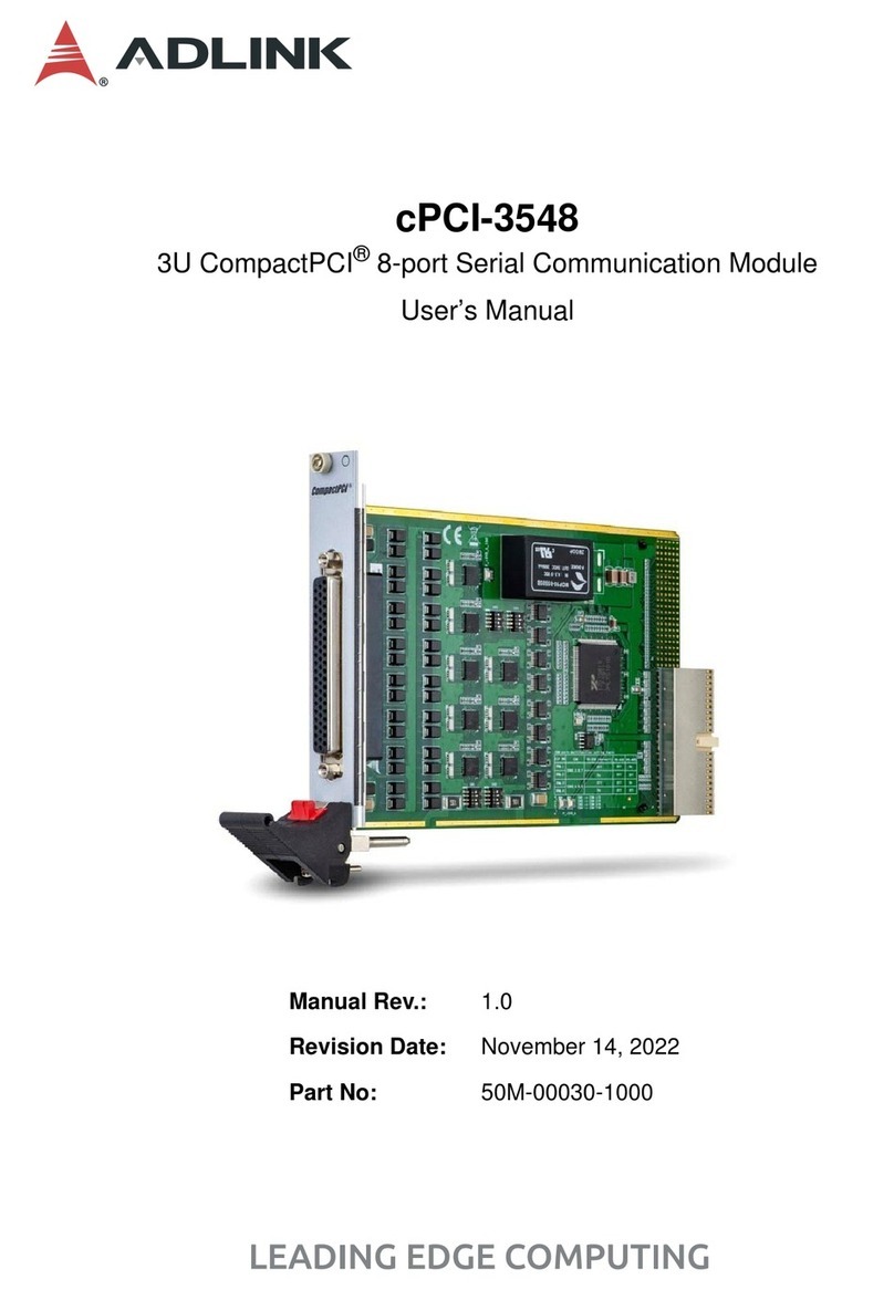
CPCI-AD32 REFERENCE MANUAL
ALPHI TECHNOLOGY CORP. Page 7REV 1.0
Part Number : 751-10-000-4000 Copyright ALPHI Technology Corporation, 1998
3.3 DSP MEMORY AND REGISTER MAP SUMMARY
NAME START END DATA R/W COMMENTS
SRAM 0x000000 0x01FFFF D00-D31 R/W Zero wait state static RAM
FLASH 0x400000 0x41FFFF D00-D07 R/W 128K x 8 Protected
A/D RESULT 0xF00000 0xF00000 D00-D31 RBoth conversion results
CONTROL1 0xF00008 0xF00008 D00-D03 WControls internal settings
CONTROL2 0xF00010 0xF00010 D00-D07 WControls internal settings
CONTROL3 0xF00018 0xF00018 D00-D00 WControls internal settings
STROBE 0xF00020 0xF00020 N/A WS Start conversion
D/A OUTPUT 0xF00028 0xF00028 D00-D31 WDAC Output register
DIGITAL
PORTS 0xF00030 0xF00030 D00-D15 R/W Bidirectional digital ports
LAST CHAN 0xF00040 0xF00040 D00-D03 WEnding channel register
MODE/GAIN 0xF00060 0xF0006F D00-D07 R/W Mode and gain per channel
AMCC 0xF00080 0xF000FF D00-D31 R/W AMCC Registers
Table 3.2: DSP Memory Map
3.3.1 A/D RESULT (Read Only)
BITS 31 - 16 BITS 15 - 00
Channel 17 – 32 Result Channel 1 – 16 Result
This 32 bit register contains the conversion results from the two A/D converters. This result
must be read during the INT2 interrupt handler, or it will be overwritten with the next
conversion result. There is no status bit to indicate completion of a conversion.
3.3.2 CONTROL1 (Write Only)
BIT 03 BIT 02 BIT 01 BIT 00
CAL_MODE EX_SCAN_EN TCLK0_EN EX_GATE_EN
EX_GATE_EN External gate enable
If this bit is set to 1, then EXGATE must be low for A/D conversions. If this bit is cleared to
0, then EXGATE has no effect.
TCLK0_EN, EX_SCAN_EN A/D
These bits determine what will trigger an A/D conversion.
EX_SCAN_EN TCLK0_EN DOUT Selection
0 0 Writes to STROBE will trigger conversion.
0 1 TCLK0 from DSP will trigger conversion.
1 0 EXTRIG will trigger conversion.
1 1 Both TCLK0 and EXTRIG will trigger conversion.
Table 3.4: Signal routing to STRB_OUT
