Anadigm AnadigmApex User manual

AN231K04-DVLP3 – AnadigmApex Development Board
UM023100-K001h Page 1 of 16
Figure 1: AnadigmApex Development Board
Disclaimer
Anadigm reserves the right to make any changes without further notice to any products herein. Anadigm makes
no warranty, representation or guarantee regarding the suitability of its products for any particular purpose, nor
does Anadigm assume any liability arising out of the application or use of any product or circuit, and specifically
disclaims any and all liability, including without limitation consequential or incidental damages. "Typical"
parameters can and do vary in different applications. All operating parameters, including "Typical’s" must be
validated for each customer application by customer's technical experts. Anadigm does not in this document
convey any license under its patent rights nor the rights of others. Anadigm software and associated products
cannot be used except strictly in accordance with an Anadigm software license. The terms of the appropriate
Anadigm software license shall prevail over the above terms to the extent of any inconsistency.
© Anadigm®, Inc. 2013
All Rights Reserved

AN231K04-DVLP3 – AnadigmApex Development Board
UM023100-K001h Page 2 of 16
1.0 Overview
The AnadigmApex development board is an easy-to-use platform designed to help you get started with
implementing and testing your analog designs on the AnadigmApex dpASP silicon devices.
While the device on this development platform is an AN231E04 device, you can use this board to implement all
of your AN131E04 and AN231E04 designs. The design software - AnadigmDesigner®2 – can use the
AN231E04 device on board to emulate the AN131E04 device thus enabling instant prototyping of your design
for either device in the AnadigmApex device family.
This manual provides an overview on how to effectively use this board to implement your analog design. But
first, here are some salient features of the AnadigmApex development board:
Features new with this revision of Development Kit board
Board footprint – 4.8 x 3.8 inches.
Standard USB serial interface for downloading AnadigmDesigner®2 circuit files.
Ability to store configurations in to onboard non-volatile memory.
Ability to store configurations in the onboard Microcontroller. Utilises Microchip PIC FLASH,
once stored this configuration can be used as the Boot circuit.
Ability to write to and then boot from EEPROM, (external EEPROM is not supplied, empty socket is
onboard).
Existing Feature (also on older boards)
Small footprint.
Large breadboard area around the AN231E04 device.
Header pins for all the dpASP device analog I/Os.
Ability to separate, electrically and physically, the digital section.
Two circuit footprints for configuration as Rauch filters, single to diff converters, level shifters etc.
Daisy chain capability – that allows multiple boards to be connected to evaluate multi-chip systems.
Standard PC serial interface for downloading AnadigmDesigner®2 circuit files.
On-board 16-MHz oscillator module.

AN231K04-DVLP3 – AnadigmApex Development Board
UM023100-K001h Page 3 of 16
2.0 Layout
Figures 2 shows the layout of the board allowing easy location of all the components, power connections and
jumpers.
Figure 2: Top-level layout of the AnadigmApex development board

AN231K04-DVLP3 – AnadigmApex Development Board
UM023100-K001h Page 4 of 16
3.0 Powering up the AnadigmApex Development Board
The options for powering up the board are as follows:
Connect a transformer with centre voltage between +4V and +12V to the jack socket input, OR
Connect wires from a single precision, regulated supply to the on-board 2-way terminal with the
voltage set to between 4V and 12V.
Anadigm recommends the use of a standard supply regulator or d.c. power supply with a regulated
output of either 6 or 9 volt d.c.
Note: the board is protected against connection to a supply with the wrong polarity
Note: The power supply “jack socket” specification is 5.5mm outer conductor, 2.1mm inner connector, inner
(or center) connector is Positive.
WARNING: the board should not be powered with more than 12.5V
There is a green LED to indicate that the board is successfully powered up. The board should take
approximately 25mA when first powered up and before the dpASP (AN231E04) is configured. The current
after the dpASP is configured depends very much on the circuit programmed into the dpASP.
4.0 Programming the board
It is possible to physically connect both the RS232 and USB cables at the same time, however only one or
the other is needed; please choose one and set the shorting link on the Development board appropriately to
enable either USB or RS232. Anadigm prefers the RS232 because it is hardware detected and
automatically discovered by AnadigmDesigner®2, we understand that many new PC’s do not have RS232
interfaces so have added a USB interface and all the complexity associated with drivers
4.1 Programming the Board (serial Interface – RS232)
Once the board has been powered up, simply connect the board to the serial port of a PC using a standard
RS232 cable. Check the position of Jumper pair J15, should be both jumpers in the upper position.
Open AnadigmDesigner®2 on the PC, create a circuit and click on Configure. If configuration is successful,
the green LED next to the PIC in the digital section will illuminate.
If the red LED illuminates then the configuration failed. If this happens then check the supply to the board
and check that the pins marked VDD have +3.3V on them. Also check that the jumpers are in their default
state (see figure 3 in section 7). Press the reset button and try again.
If configuration was successful then the circuit created in AnadigmDesigner®2 will be programmed into the
dpASP. The analog inputs and outputs can be accessed via the header pins that surround the dpASP.
Note that the outer rings of pins are connected to the dpASP analog I/Os, the inner ring of pins are all
connected to VMR which is at analog signal ground (+1.5V).
4.2 Programming the Board (USB serial Interface)
Introduction
The AN231K04-DVLP3 Ver3 board uses a Silicon Labs USB to UART Bridge, this device uses a standard
USB cable, installs like a USB port but internally to the PC and software it appears as a Serial port.
Check the position of Jumper pair J15, should be both jumpers in the upper position.
Driver Installation
Do not connect the AN231K04-DVLP3 Ver3 board to your PC via the USB cable nor start the AN231K04-
DVLP3 Ver3 board GUI at this time - the driver must be installed first.
It is assumed that AnadigmDesigner®2 is already installed and registered on your PC.
To install the drivers (CP210x_Drivers.exe) included on the AnadigmDesigner®2 CD. You can also find the
driver here http://www.anadigm.com/sup_downloadcenter.asp?tab=des&offset=15
If this is your first use and you do not have any previous drivers installed start from 3) below.
1) Unplug any USB connected AN231K04-DVLP3 Ver3 board and if applicable other Anadigm product or
SiliconLabs CP210x devices.

AN231K04-DVLP3 – AnadigmApex Development Board
UM023100-K001h Page 5 of 16
2) Remove old drivers that have previously been installed. For Windows systems, open the Add or Remove
Programs window from the Control Panel. Next, select each CP210x entry and click on Remove.
3) Run the driver executable, CP210x_Drivers.exe, to extract the device drivers included with this release
(this application is tested with Windows Only). The default installation directory for these extracted files is
"C:\Silabs\Mcu\CP210x". To complete the driver installation……..
4) Connect the AN231K04-DVLP3 Ver3 board and power it.
5) Install the new drivers. For Windows systems, the Add New Hardware Wizard should open when this
new device is detected. Use the wizard to install the drivers by directing it to the
"C:\SiLabs\MCU\CP210x\WIN" directory created in step 3.
The hardware wizard will install CP210x Composite device, then the CP2102 USB to UART Bridge
Controller Drivers.
The drivers are now installed, connect a powered AN231K04-DVLP3 board, start the AnadigmDesigner®2,
from your desktop and check the connection from your AnadigmDesigner2 on you PC to the AN231K04-
DVLP3 Ver3 board GUI is working correctly.
From within AnadigmDesigner2, go to “settings/preferences” and choose the “Port” Tab.
If the installation has been successful the dropdown Port select menu will allow you to select
COM* - CP2101 USB to UARF Bridge Controller,
(COM* - * this number will be depend on you PC configuration).
NOTE: Driver installation and Port selection is only needed ONCE.
If you subsequently plug into a different USB controller on your PC you may need to repeat step 5.
Board use – following driver installation is same as with the RS232 port.
Open AnadigmDesigner®2 on the PC, create a circuit and click on Configure. If configuration is successful,
the green LED next to the PIC in the digital section will illuminate.
If the red LED illuminates then the configuration failed. If this happens then check the supply to the board
and check that the pins marked VDD have +3.3V on them. Also check that the jumpers are in their default
state (see figure 3 in section 7). Press the reset button and try again.
If neither LED illuminates and AnadigmDesigner®2 reports a communication error, then check from
Anadigm Designer2
If configuration was successful then the circuit created in AnadigmDesigner®2 will be programmed into the
dpASP. The analog inputs and outputs can be accessed via the header pins that surround the dpASP.
Note that the outer ring of pins are connected to the analog I/Os, the inner ring of pins are all connected to
VMR which is at analog signal ground (+1.5V).

AN231K04-DVLP3 – AnadigmApex Development Board
UM023100-K001h Page 6 of 16
5.0 Evaluating Multi-chip Designs – Daisy Chaining
Figure 3 shows an example of how to chain 2 boards together. More boards can be chained using the
instructions shown in this figure.
Figure 3: Positions of Jumpers and Default Settings

AN231K04-DVLP3 – AnadigmApex Development Board
UM023100-K001h Page 7 of 16
6.0 Other Features
6.1 VREF Pins
The 3 reference pins on the dpASP device – VMR (+1.5V), VREFP (+2.5V) and VREFN (+0.5V) – have been
connected via the p.c.b. tracks to the 3 holes to the right of the dpASP (see figure 2). In addition, VMR is available
on the inner ring or inner two rows of pins that are adjacent to the analog I/Os.
NOTE: These reference voltages are not designed to provide current.
6.2 Header Pins
All of the analog I/Os of the dpASP are brought out to header pins for easy connection. Next to these header pins is
a second row of header pins connected to VMR (+1.5V). This allows the user to connect any dpASP analog I/O to
VMR using shorting jumpers, resistor jumpers or capacitor jumpers. A shorting link (jumper) should only be used
when the I/O cell is configured as an input. Damage may occur to the device if an output if shorted to VMR.
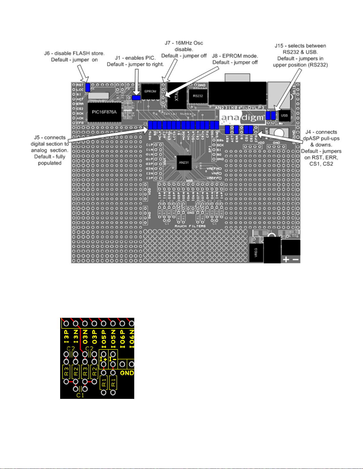
6.3 EPROM
There is an SPI EEPROM socket in the digital section of the board. To put the board into EEPROM mode, starting
from the default jumper position (detailed below, section 7):
1. Put a jumper onto J8 which sits right next to the EPROM socket, and
2. Put a jumper on J4 in the position marked SI so that this pin is connected to a pull-down.
3. Make sure that there are jumpers on J5 in the positions marked GND, VDD, CFG, ACLK, SI, MCLK and SO
(it is OK to put jumpers in all positions of J5).
4. Move the jumper on J1 to the left to disable the PIC.
Press the “reset” button to download the circuit from the EPROM into the dpASP.
Note that an EEPROM integrated circuit is not supplied with this Development Kit. If you wish to use an SPI
EEPROM, source one and place it in to the socket on the board. An example of a compatible SPI EPROM is the
Atmel AT25080.
To write the EPROM follow this procedure:
1. With the board powered down, place a jumper on J8 to put the board in EPROM mode.
2. Make sure that the jumper J1 is placed to the right to enable the PIC.
3. Make sure that there is no jumper on J6 (FLASH storage must be enabled to write the EPROM).
4. Remove the jumpers marked MCLK and SO from the digital interface J5.
5. Power up the board and configure it in the usual way with the circuit that is required to be stored in EPROM.
6. Power down the board and replace the jumpers marked MCLK and SO on the digital interface J5.
7. Move the jumper J1 to the left to disable the PIC.
8. Keep the jumper on J8. Also make sure that there is a jumper on J4 in the SI position.
9. Power up the board and it will configure from the EPROM. Resetting the board will also cause it to be
configured from the EPROM. Note that there will be no LEDs lit to show that the configuration was successful.
This is because the LEDs are driven by the PIC and this is disabled when booting from EPROM.
*NOTE: before configuring the board, a setting needs to be changed in AnadigmDesigner®2 if the circuit is to be
stored in EPROM. To change this setting, go to the Settings menu in AnadigmDesigner®2, select Active Chip
Settings, then select the Chip tab. In the pull-down menu labelled “How is this mode pin connected on the target
board?” select “Mode pin has been tied high (VDD)”. Click on OK. Then configure the board. If an EPROM
programmer is used to program the EPROM, this setting still needs to be changed in AnadigmDesigner®2 before
generating the data for programming into the EPROM.
6.4 Reset Button
There is a reset button near the upper right corner of the board. This resets both the dpASP and the PIC (unless
the PORb jumper is removed from J5 or the J1 jumper is in the left position).
In EPROM mode, press the reset button to load the circuit from the EPROM into the dpASP.
6.5 SPI Port
There is an SPI port for direct control of the dpASP by an external SPI controller. Note that all the jumpers should
be removed from J5 when the SPI port is used. (see the AN231E04 dpASP specification and use guide for details
of this SPI connection)

AN231K04-DVLP3 – AnadigmApex Development Board
UM023100-K001h Page 8 of 16
6.6 Digital Section
The digital section of the evaluation board is provided only so that there is a convenient (serial) interface from the
board to a PC to enable direct configuration (instant prototyping) of the dpASP from AnadigmDesigner®2 software,
normal use of the dpASP does not require this digital interface, the dpASP can be programmed directly from an SPI
interface. It is convenient when first developing an analog circuit within the dpASP to have the direct interface to
AnadigmDesigner®2, when the circuit(s) are implemented into a final design either a host uP (or DSP) or an
EEPROM is normally used to store and configure the dpASP.
The digital section of the board includes an RS-232 transceiver, a USB transceiver and a PIC microcontroller (to
perform serial ASCII to bit conversion). It also includes a green LED (to indicate successful configuration), and a
red LED (to indicate failed configuration).
The digital section sits along the top side of the board and is connected to the rest of the board by a set of jumpers
J5. It is possible to cut away the digital section to leave a purely analog board with header pins on the edge to
provide an external digital interface.
If the digital section of the development board is removed or ignored (by pulling jumpers J5), the dpASP can be
configured directly using any processor with an SPI interface (or port configured with appropriate signals) by
connecting signals directly to the dpASP side of J5 or by connecting to the set of pins marked “SPI”. Full dynamic
control of the dpASP’s analog circuitry can be realised under software control via this connection.
Note
Anadigm®does not recommend any specific processor/controllers – our products work with most processors.
Anadigm®recommends that our customers use their own processor development boards and connect via jumper
J5 to Anadigm’s dpASP for fully dynamic control of the dpASP, in preference to re-engineering the digital section of
this development board.
6.7 FLASH Storage
In FLASH storage mode, all primary configurations sent to the development board are stored in the FLASH of the
PIC. The last configuration sent will be stored. This means that after the board has been configured, it will
remember the last configuration it was sent after being reset or board power being cycling off and on. Note that
when chaining boards, the primary configurations for all devices in the chain will be stored. Reconfigurations are not
stored.
The FLASH memory can be cleared by briefly shorting the jumper J6.
If FLASH storage of primary configurations is not wanted then a jumper should be placed permanently on J6 to
disable this feature.

AN231K04-DVLP3 – AnadigmApex Development Board
UM023100-K001h Page 9 of 16
7.0 Jumpers
Table 1 shows a complete list of the jumpers on the board and figure 4 shows their positions.
Jumper Function Default State Default Condition
J1 This jumper allows the MCLRb pin of the PIC to
either be connected to the PORb pin of the dpASP
or to be grounded. Grounding the MCLRb pin
tristates all of the PIC I/Os and thus allows
connection of another controller or EPROM to the
digital pins of the dpASP. Useful for daisy chaining
boards where one PIC controls 2 or more dpASPs,
and also for using an EPROM.
Jumper to right MCLRb pin of PIC is
connected to PORb
pin of dpASP.
J4 Connects pull-ups and downs to some of the dpASP
digital pins, or ties CS1b low. A jumper in place
connects the pull-up/down in the following way:
POR – 10k pull-up on PORb
ACT – 10k pull-up on ACTIVATE
ERR – 10k pull-up on ERRb
SI – 10k pull-down on SI
CS1 – ties CS1b low
CS2 – 10k pull-down on CS2b
CFG – 10k pull-up on CFGFLG
Jumpers on POR,
ERR, CS1 and CS2 PORb is pulled high,
ERRb is pulled high,
CS1b is tied low and
CS2b is pulled low.
J5 Connects the digital section to the analog section All 15 jumpers
should be on. Fully connects power,
ground and all dpASP
digital signals to the
digital section.
J6 Disables the storage of primary configurations in the
PIC’s FLASH. If the jumper is left off, the board will
remember the last primary configuration after reset
or power cycling. Briefly shorting this jumper will
cause the configuration memory to be cleared.
Jumper on Not in primary
configuration storage
mode.
J7 A jumper on J7 will disable the 16MHz oscillator
module and tristate its output. This means that the
ACLK pin of the dpASP will not be clocked. Useful in
daisy chaining boards where the ACLK pin of 2 or
more dpASPs should be driven by one source.
Jumper off 16MHz oscillator
enabled.
J8 A jumper on J8 enables EPROM mode.
Boot from EPROM, SPI master mode.
Also allows writing of configurations to the EPROM.
Jumper off Board in micro mode
(SPI is a slave).
J15 2 jumpers select if the board is in RS232 mode or
USB mode. Place both jumpers in the upper position
for RS232, in the lower position for USB.
Both jumpers in
upper position Board in RS232
mode.
Table 1: Summary of Development Board Jumpers

AN231K04-DVLP3 – AnadigmApex Development Board
UM023100-K001h Page 10 of 16
Figure 4: Positions of Jumpers and Default Settings
8.0 Rauch Filters
The AN231K04 printed circuit board has an available option for you to use to add Rauch filters, at either the analog
input signal path, output signal path or neither. Figure 5 details two suggested Rauch filter circuits.
These can be easily implemented by adding appropriate components to the
p.c.b.. This picture of the p.c.b show’s an example of one of two p.c.b. layouts,
for resistor and capacitor placement.
The default signal connection is directly to the header pin connected to the
AN231E04 dpASP. To use these filters add the correct components and
connect the signal input or output appropriately.
The math associated with a typical low pass input filter is also provided here.

AN231K04-DVLP3 – AnadigmApex Development Board
UM023100-K001h Page 11 of 16
Figure 5: Suggested Rauch filter circuits
For low pass response:
H(s) = 1/((R1/R2)+ (sC2(R1+R3+(R1*R3/R2)))+
(s2R1R3(2.C1)C2))
R1 = R2 = 2R3 = 2R
And
C1 = 2C2 = 2C
Fc = 1/(4πRC(SQRT 2))
Re-arranging these equations for low pass filter
R1 = Rin;
R2 = G*Rin;
R3 = G*Rin;
C1 = Q.(G+1)/(G.4.π.Fo.Rin);
C2 = 1/(G.4.π.Fo.Q.R1)
Examples
Rauch filter settings:
For Fc = 30kHz:
R1=R2=10k, R3=5k, C1=0.75nF, C2=0.375nF
For Fc = 40kHz:
R1=R2=10k, R3=5k, C1=0.56nF, C2=0.28nF
For Fc = 10kHz
R1=R2=10k, R3=5k, C1=2.2nF, C2=1.1nF
Alternative math.
C1=2.C2.(G+1).Q^2 R1=1/(Q.4.G.π.F.C2) R2=G*R1 R3=1/(Q.4.(G+1).π.F.C2)
from these : C1=Q.(G+1)/(2.G.π.F.R1) and C2 = 1/(G.π.F.R1.4.Q)
Example,
Starting from a requirement for a corner frequency of 10kHz and we want a gain of 1
Choose to use 10kohm resistors
so that R1=R2=10k,
also if we choose a Q=0.707 for flat response then:
C1=1.414/(2 x πx 10k x 10k) = 2.25nF
and C2=1/(1 x πx 10k x 10k x 4 x 0.707) = 1.1nF
and R3=1/(0.707 x 4 x 2 x πx 10k x 1.1n) = 5.1kohm

AN231K04-DVLP3 – AnadigmApex Development Board
UM023100-K001h Page 12 of 16
9.0 Absolute Maximum Ratings
Parameter Symbol Min Typ Max Unit Comment
DC Power Supply
3.5mm jack socket
Vjack 4 9 12.5 V DC voltage only
Centre pole is positive, outer sleeve is
ground
DC Power Supply
Screw terminal “+” post
V+ 4 9 12.5 V DC voltage only
Voltage is relative to “Gnd” post
DC power Supply
regulator, max current,
12volts input
Isupply - 150
100
mA
mA
At room temperature
At 50oC
The dpASP require typically 40mA (max
70mA) The additional available additional
power may be used for components you
may add to the breadboard area.
The current is limit by the regulator power
dissipation.
dpASP Input Voltage Fin -0.5 +3.6 V Direct input to dpASP on analog IO
header pins or digital pins (J5)
dpASP Output Voltage Fout -0.5 +3.6 V Direct output from dpASP on analog IO
header pins or digital pins (J5)
RS-232 Input Voltage Rin -30 +/-10 +30 V Standard RS-232 signal levels
RS-232 Output Voltage Tout -15 +/-10 +15 V Standard RS-232 signal levels
Operating Temperature Top 10 50
oC Ambient Operating Temperature,
At 50oC the power regulator is only
capable of supplying 100mA, this is
sufficient for the dpASP device but will not
support a lot of exteral components on the
breadboard area.
Storage Temperature Tstg -20 70
oC Ambient Storage Temperature

AN231K04 – the AnadigmApex Development Board
UM023100-K001h Page 13 of 16

AN231K04 – the AnadigmApex Development Board
UM023100-K001h Page 14 of 16

AN231K04-DVLP3 – AnadigmApex Development Board
UM023100-K001h Page 15 of 16

AN231K04 – the AnadigmApex Development Board
UM023100-K001h Page 16 of 16
Notes:
For More information Contact
http://www.anadigm.com
This manual suits for next models
1
Other Anadigm Motherboard manuals