RangeMaster5 Evaluation board – Quick start Guide
DS0238K08-U005a
Quick start instructions:
1. The initial state of the digital inputs should be described in the following table. Initial State refers to the electrical
signal present on these connection points immediately after connecting the 3.3volt power source.
In/Output Initial state Comments
EXEC low This pin has a 10K pull-down resistor.
SCK low This pin has no pull-down and must be driven low.
SDI high or low This pin has no pull-up or pull-down so should be driven, but which state is not
important.
SSb high This pin has no pull-up and must be driven high.
RSTb high This pin has a 10K pull-up resistor. To Reset the board momentarily pull RSTb low,
Minimum low time = 10 msec
BUSY low This pin is an output, At start-up will drive high whilst the board is configuring; start-up
configuration time is approx 36msec.
When configuration has completed this pin pulls low.
When a re-configuration word is received this pin will drive high until configuration is
complete
2. Apply power to the board +3.3V. The RangeMaster5 board will immediately start to configure itself, after about 36ms
this will be complete the board then puts itself into /Sleep standby mode”. Do not enter a Control word during this
initial 36msec configuration period. The BUSY output will drive high during this time.
3. To wake the board from standby/sleep mode, input any 16 bit control word followed by the correct 16 bit control word.
The contents of this first control word will be ignored they are used only to “wake-up” the board. A control word is
entered using SCK, SDI and SSb, and must be entered as two separate bytes according to the timing diagram in
figure 6, page 26 of the RangeMaster2 datasheet and on the next page. After the wake-up control word has been
entered, a second new control word should not be entered for at least 30us after the end of the wake-up control word.
Note that the BUSY signal will drive high during this period to indicate that the system is busy. When BUSY goes low,
it is safe to enter another control word. Now the board is awake. To put the board into the desired configuration
requires entering the appropriate control word, again entered as 2 bytes, conforming to the timings given in the
datasheet. The RangeMaster5 control byte is detailed on page 25 of the RangeMaster5 datasheet and is below; the
meaning of each bit in the control word is defined. Note that the time taken for the board to reconfigure itself after a
new control word can be anything from 1 to 50msec, so the time between control words should be at least 50msec,
unless the first control word is a wake-up in which case there should be a delay of just 30us before the next control
word is entered. Note that the BUSY signal will drive high after each control word is entered to indicate that the
system is busy. When BUSY goes low, it is safe to enter another control word. If the board is functioning correctly,
then in normal operation the VMR pin should be at +1.5V. In standby mode this pin should be at 0V.
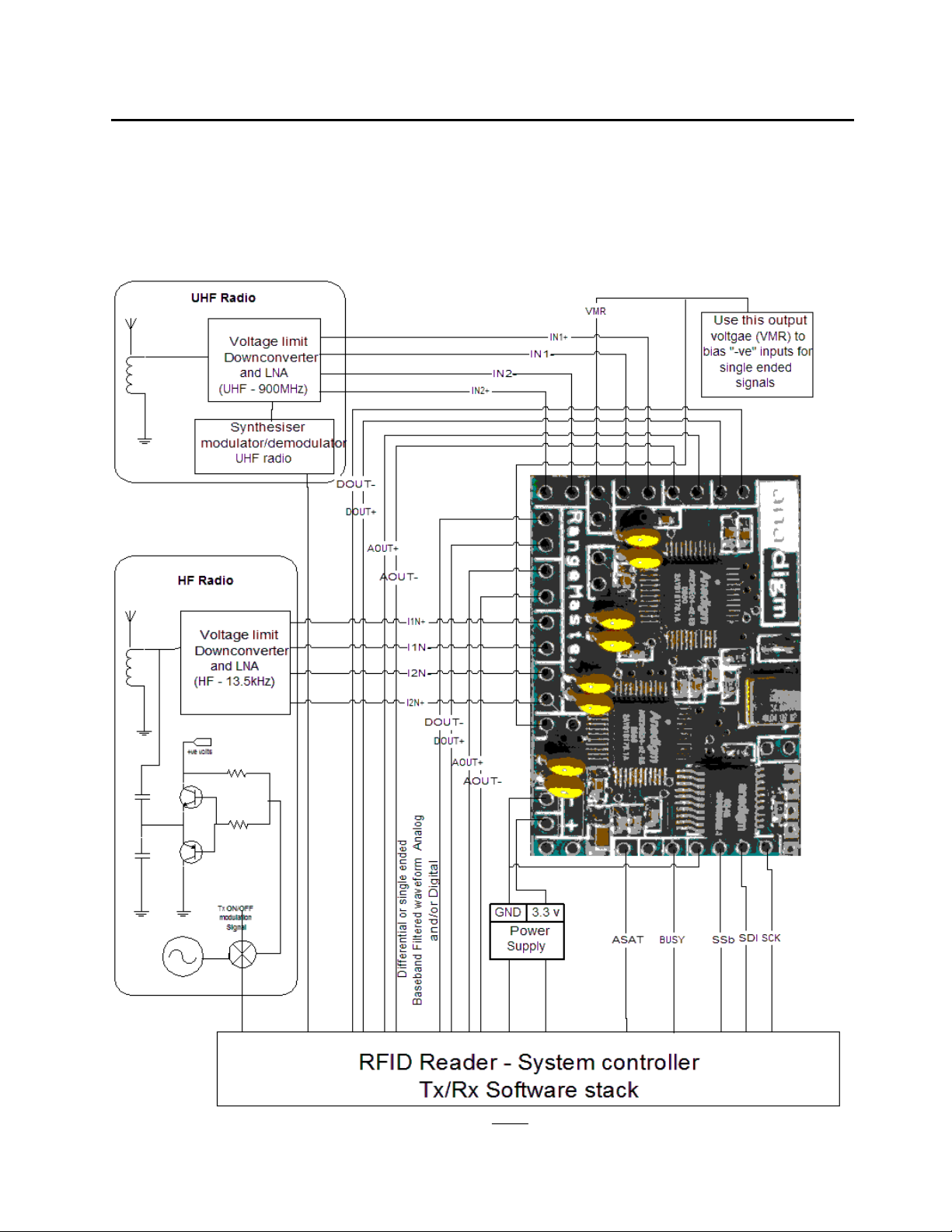
4. The differential input signal should be connected to IN1+ and IN1- (or IN2+ and IN2-). The differential amplitude of
this signal should not exceed +/-2.9V (minimum 5mV). The input connections are wired to the dpASP (AN231E04)
device via a pair of 100nF capacitor (this provides a.c. coupling), but also adds a time constant, you may want to
adjust the value of these capacitors for the higher frequency signals.
5. If the input signal is single ended, connect it to IN1+ (or IN2+) and connect IN1- (or IN2-) to VMR by shorting the VMR
hole to the hole above it (a jumper can be fitted if required). See figure2.
6. The output will appear as a differential signal with +1.5V common mode voltage on AOUT+ and AOUT-. A digitized
version of this signal will appear on DOUT+ and DOUT-.
7. If a singled ended output signal is required connect to AOUT+ or DOUT+ and ignore the –ve output, the amplitude of
the output signal will be half that of a differential output and will have a d.c.offset of +1.5volts. (fig3)
8. The board can be put back into standby mode by entering a zero control word i.e. 0x0000. Note that any control word
will wake the board from standby, so repeated inputting of a zero control word will cause the board to toggle in and
out of standby.
9. The board can be reset either by power cycling it or by pulsing RSTb low for a minimum of 10ms. There is a hole next
to RSTb which is connected to ground. This allows a jumper to be fitted if required.
Note: Analog signal path within the AN238E04 has an additional start-up delay
When changing circuit parameters the Analog signal path will be reconfigured immediately after the BUSY line drives
low. At start-up, following Reset and when changing circuits (e.g. from “wide” to “twin”, the Analog signal
path within the AN238E04 device will be active 55msec after the State Machine (AN238C04) busy line drives
low.
Page 2