Evaluation Board User Guide UG-467
Rev. 0 | Page 7 of 12
INPUT CURRENT
Measuring Total Input Current (IVIN)
When measuring VINx input quiescent currents, take into
account that the evaluation board includes an LDO (U1) and
I2C input/output (I/O) expander (see U2 and U3A in Figure 8).
The LDO generates a 3.4 V VDDIO voltage for the I2C bus and
SYS_EN open-drain output, and the I/O expander controls
digital inputs DIG_IO1, DIG_IO2, and DIG_IO3.
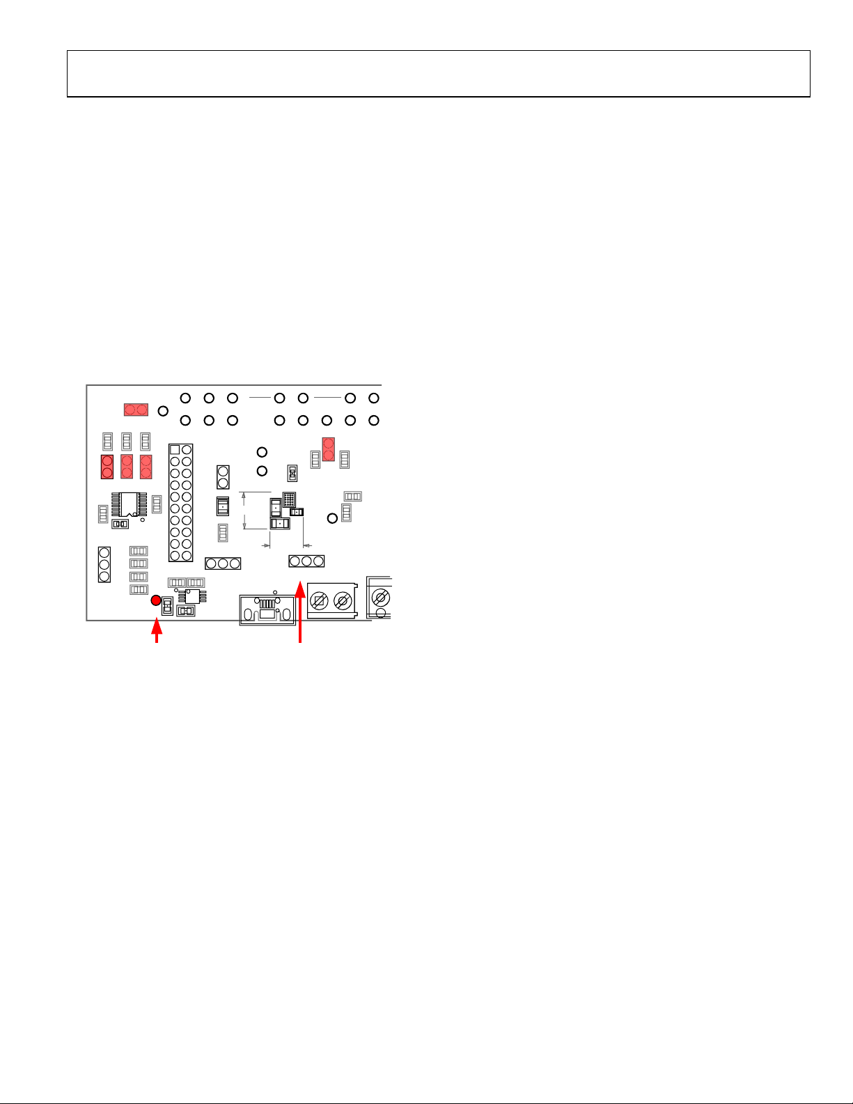
In the ADP5061 evaluation board typical setup, the U1 and the
U3 are powered through a pin header, J3. Typically, the combined
current consumption of the U1 and the U3 are in the range of
1 mA to 2 mA. To separate the evaluation board quiescent
current from the ADP5061 VINx quiescent current, leave J3
open and connect a second dc power supply (3.5 V to 5.0 V)
to the TP5 test point (see Figure 6).
J1
1
2
J4
JP2
C4
C5
C3
U2
C1
C2
D1
J11
J3
JP1
J2
9
8
7
21
1
17
16
TP15
14
13
12
11
10
1
TP4
TP3
TP6
TP5
TP20
C12
C6
U1
U3
J9
J8
J10
J7 J6
J5
R18
R17
R16
R9
R6
R13
R5
R2
R8
R15
R14 R1
R7
R12
R11
R10
7.2mm
CBP
8.4mm
SYS_EN
BAT_SNS
VCO_LDO
ISO_
ISO_S_S
D3D1D2
ILED
ISO_S_F
VDDIO
D3 D2 D1
THR
VIN_F
GND
ILED
GND
GND
GND
D3SD3
D1S VIN_F
ISO_S_F GND
ISO
ISO
ISO
ISO
ISO
VIN_S GND_STHR
ILED_S
ISO
D2S
D2
D1
VIN_S
SDA
VIN_F
SCL
OPEN J3
CONNECT 3.5V – 5V
SUPPLY ON TP5 TO
POWER U1 AND U3
10993-016
Figure 6. Board Setup for VINx Quiescent Current Measurement
VINx Current Limit
The VINx current limit of the ADP5061 can be evaluated in
charging mode. Note that the maximum programming for
the charge current into the battery (ISO_Bx) is 1300 mA. For
measuring the input current limit across the full programming
range from 100 mA to 2100 mA, additional system load has to
be connected to the ISO_Sx pins.
To measure the VINx current limit, do the following:
1. Set the VVIN supply voltage to 5.0 V.
2. Set the VISO_B voltage to 3.6 V on SMU B.
3. Enable charging by setting Register 0x07, Bit D0
(EN_CHG), to high.
4. Confirm that the ADP5061 is in charging mode by the
following:
•The Battery Status indicator on the GUI must show
BAT_SNS > Vweak (see Figure 2).
•The ADP5061 must start charging 80 mA to 90 mA
current into the battery.
5. Measure the current on VINx supply.
6. Use the GUI to change the input current limit programming
and repeat the measurement.
A 1300 mA charge current into the battery may not be large
enough to drive the input current up to the limit when the
current limit programming values of 1200 mA or higher are used.
Connect an additional load on the ISO_Sx node to evaluate the
higher end of the input current limit programming range.
TRICKLE CHARGE CURRENT
Trickle charge can only be activated during a battery charging
startup sequence, if the voltage level at the ISO_Bx pins is lower
than the VTRK_DEAD threshold (typically 2.5 V). When VVIN is 5.0 V,
initiate a charge startup sequence by setting an I2C write of
Register 0x07, Bit D0 (EN_CHG), high. To measure the trickle
charge current level, do the following:
1. Set the VISO_B voltage (SMU or battery simulator) to 2 V.
2. Set the VIN supply voltage to 5.0 V.
3. Check that the GUI Charger Status indicator shows
Trickle Charge.
4. Check that the GUI Battery Status indicator shows
BAT_SNS < Vtrk.
5. Check the battery short detection by doing the following:
•Wait for a 30 second timeout to expire
•Check that the GUI shows that the I2C fault register
(Register 0x0D, Bit D3) BAT_SHR flag is set.
•Use the GUI to change the battery short timeout
setting from 1 second to 180 second.
6. Measure the trickle charge current level to the battery. The
default value for ITRK_DEAD is 20 mA. It is possible to change
the trickle charge current setting from 5 mA to 80 mA
using the GUI.
7. Adjust the VISO_B voltage up until the Battery Status indicator
shows Vtrk < BAT_SNS < Vweak.
8. The Charger Status indicator on the GUI should show Fast
Charge (CC-Mode). The charge current is now programmed
ICHG + ITRK_DEAD, if it is not limited by the input current limit.