manuals.online logo
Brands
  1. Home
  2. •
  3. Brands
  4. •
  5. Andrew O'Malley
  6. •
  7. Clock
  8. •
  9. Andrew O'Malley DOTKLOK User manual

Andrew O'Malley DOTKLOK User manual

Popular Clock manuals by other brands

Sapling NTP 7000 Series installation manual

Sapling

Sapling NTP 7000 Series installation manual

Amano MTX-30F Installation & operation guide

Amano

Amano MTX-30F Installation & operation guide

La Crosse Technology BBB86118v3 Setup guide

La Crosse Technology

La Crosse Technology BBB86118v3 Setup guide

BEARWARE 304474 manual

BEARWARE

BEARWARE 304474 manual

LS & S RTC103U instruction manual

LS & S

LS & S RTC103U instruction manual

BitGen Technologies LED Walk/Don't Walk Clock user manual

BitGen Technologies

BitGen Technologies LED Walk/Don't Walk Clock user manual

Heathkit GC-1005 Assembly manual

Heathkit

Heathkit GC-1005 Assembly manual

Oregon Scientific PRYSMA RMR221P manual

Oregon Scientific

Oregon Scientific PRYSMA RMR221P manual

Nixie Clock Divergence Meter user manual

Nixie Clock

Nixie Clock Divergence Meter user manual

La Crosse Technology WS-8256-AL user manual

La Crosse Technology

La Crosse Technology WS-8256-AL user manual

Mini Gadgets MCPro user manual

Mini Gadgets

Mini Gadgets MCPro user manual

Casio TMR-200 user guide

Casio

Casio TMR-200 user guide

Progetti KALIMERO Directions

Progetti

Progetti KALIMERO Directions

Progetti ILTEMPOSTRINGE Directions

Progetti

Progetti ILTEMPOSTRINGE Directions

La Crosse Technology WT-3141b Quick setup instructions

La Crosse Technology

La Crosse Technology WT-3141b Quick setup instructions

IKEA ROTBLÖTA manual

IKEA

IKEA ROTBLÖTA manual

U-Line Н-2811 instructions

U-Line

U-Line Н-2811 instructions

Silicon Laboratories SI5324 manual

Silicon Laboratories

Silicon Laboratories SI5324 manual

manuals.online logo
manuals.online logoBrands
  • About & Mission
  • Contact us
  • Privacy Policy
  • Terms and Conditions

Copyright 2025 Manuals.Online. All Rights Reserved.

D O T K L O K Assembly Instructions
1 January 2015
www.technoetc.net/dotklok / www.andrewomalley.etsy.com
Required tools / materials
•soldering iron
•solder
•wire strippers
•flush cutters / wire nippers / diagonal cutters
•multi-bit screwdriver
•small / needle-nose pliers
O tional tools / materials
•helping hands
•solder fan / defumer
•multi-meter
•solder sucker/vacuum
•solder wick
•lint-free / microfiber cloth
PART I: PCB ASSEMBLY
Your final PCB will look like this, once fully assembled
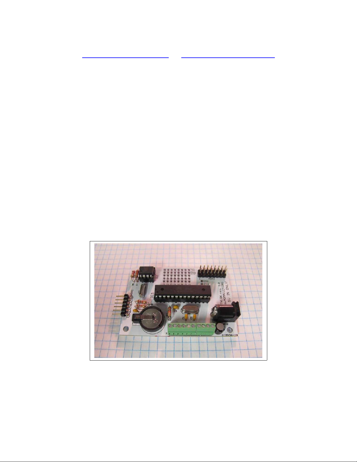
All parts sit on the top of the board and are soldered from the bottom.
Please refer to the bill of materials (BOM):
www.aomalley.org/dotklok/files/DOTKLOK_bom_illustrated.pdf
for an illustrated parts list.
Take care when unpacking the kit components, there are several small parts,
and no extras have been provided. TIP: the foam housing for the LED screen
makes for a handy parts tray while assembling DOTKLOK.
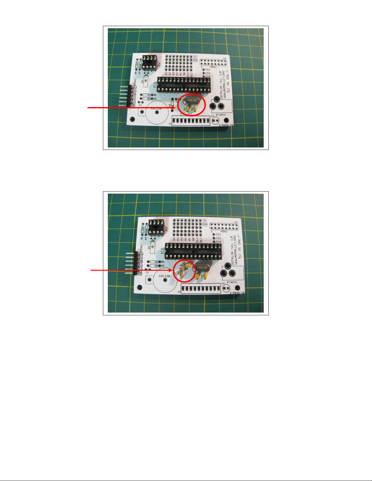
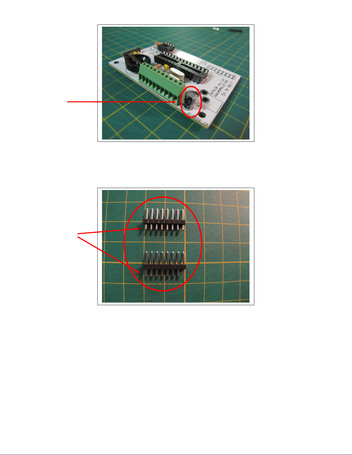
If your PCB is labeled “DOTKLOK . ” you will need to solder a wire
across the JP pads in order for the board to work with the power supply
included with your kit. Although a specific wire has not been included for
soldering this jumper, you can can use one of the cut-off leads from a
resistor or capacitor soldered in the following steps.
2
Solder a wire
across JP
. Solder HDR (six pin, right-angle header, no polarity), with long pins facing
out from PCB.
2. Solder SK2 (small, 8 pin chip holder) at IC2 and SK (large, 28 pin chip
holder) at IC , matching the notch of the chip holder with the notch on
the PCB diagram.
3
Note, notches
(circled) must match
by facing
left
Note, long pins
facing out from
PCB
3. Solder Q ( 6Mhz crystal, no polarity), C and C2 (22pF capacitors, no
polarity, marked 220). If needed, bend leads to hold components in board
during soldering; once soldered, trim excess leads from back of PCB.
4
SK2 (small 8 pin
chip holder) at
IC2. Note, notch
(dotted circle)
faces left
Bent leads best
hold
components in
while soldering;
Excess leads
should then be
trimmed
SK (large 28
pin chip holder)
at IC . Note,
notch (dotted
circle) faces
left
4. Solder R3 ( 0k resistor, no polarity, colour bands: brown-black-orange)
and C5 (0. uF capacitor with long leads, no polarity, marked 04), trim
excess leads from back of PCB.
5
Q ( 6Mhz crystal)
with C and C2
(22pF capacitors)
R3 ( 0k resistor)
and C5 (0. uF
capacitor)
5. Solder R and R2 ( k resistors, no polarity, colour bands: brown-black-
red) and C3 (0. uF capacitor with long leads, no polarity), trim excess
leads from back of PCB.
6. Solder R4 and R5 (2.2k resistors, no polarity, colour bands: red-red-red),
trim excess leads from back of PCB.
6
R and R2 ( k
resistors) and
C3 (0. uF
capacitor)
R4 and R5 (2.2k
resistors)
7. Solder CR 220 (coin cell holder). Note, coin cell holder must be placed
so that the square edge points left.
8. Solder X ( 0 position screw connector). Openings MUST face outer
edge of PCB.
7
CR 220 (coin
cell holder). Note,
square edge
points left
X ( 0 position
screw connector)
opening MUST be
placed so open
part faces outer
edge of PCB as
shown in the red
circle. The
connector should
NOT be placed
with the closed
end facing the
outer edge (as
shown in the
crossed out
picture)
FAIL
9. Solder C4 ( 0uF olarized capacitor), making sure (longer) positive lead
(black side of cap) goes into square (left) pad. (Note: the negative side of
the cap is marked with a silver/grey stripe); trim excess leads from back
of PCB.
8
X ( 0 position
screw connector).
Note, open part
faces outer edge
of PCB
C4 ( 0uF
capacitor) is
polarized. Longer
(positive) lead is
marked by the
black side; shorter
(negative) lead is
marked by the
grey side
0. Solder HDR2 (two separate 8-pin upright headers) Short leads MUST go into
the board for soldering; taller leads MUST face upright, coming up from top of
board. Ensure headers are soldered so they are straight and upright. You do not
want them to be crooked.
9
C4 ( 0uF
capacitor) longer
(positive) lead
(marked by the
black side) MUST
go into the square
(left) pad on the
board
Short leads MUST
go into the board
for soldering
. Solder Q2 (32.768kHz crystal, no polarity). Important, push the crystal
ONLY half way down into the board. Solder and trim excess leads from
back of PCB. Then, gently bend crystal down against PCB to match
diagram on PCB.
0
As best as
possible, ensure
headers are
soldered so they
are straight and
upright. You do not
want them to be
crooked
Push the Q2
(32.768 kHz
crystal) ONLY ½
down into the
board so that half
of the leads can be
seen from the top
of the board