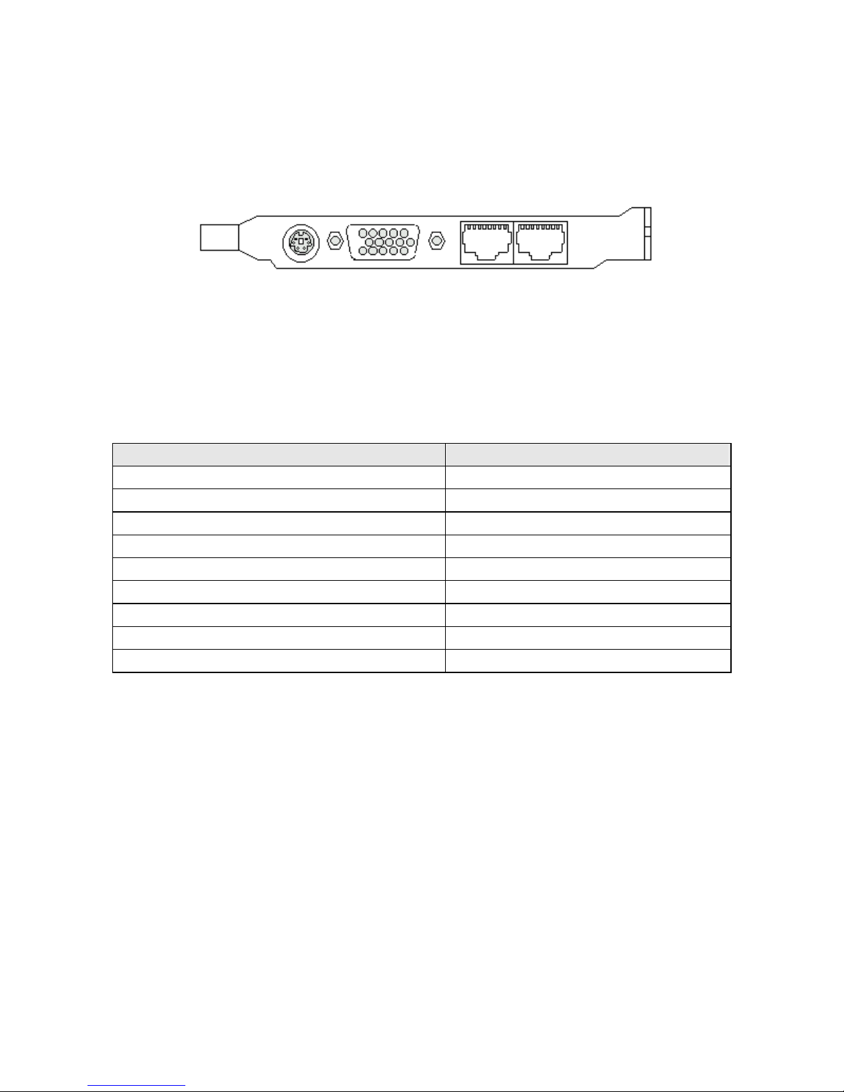
aone FBX2 SERIES User manual

FBX2
Series
(Full-Size Single Board Computer)
INSTALLATION GUIDE
Installation Guide Revision A.1
60002F2A1


i
COPYRIGHT©
All rights reserved. The information contained in this guide has been
validated and reviewed for accuracy. No patent liability is assumed with
respect to the use of the information contained herein. While every
precaution has been taken in the preparation of this guide, the Manufacturer
assumes no responsibility for errors or omissions.
No part of this publication may be reproduced, stored in a retrieval system, or
transmitted in any form or by any means, electronic, mechanical,
photocopying, recording, or otherwise, without the prior written permission of
Manufacturer.
TRADEMARK™
Intel®, Pentium®and MMX®are registered trademarks of Intel®Corporation.
Microsoft®and Windows®are registered trademarks of Microsoft
Corporation.
All products and company names are trademarks or registered trademarks
of their respective holders.
These specifications are subject to change without notice.
Installation Guide Revision A.1
January 2002

ii
CONTENTS
SECTION 1 INTRODUCTION 1
1.1 Unpacking FBX2 Series 1
1.2 Description 3
1.3 Features 3
1.3.1 Hardware Monitoring 3
1.3.2 I/O Shield Connector 4
1.3.3 FBX2 Series Overview 5
1.3.4 System Block Diagram 5
1.4 Specifications 6
SECTION 2 INSTALLATIONS 8
2.1 System Installation 8
2.1.1 CPU Installation 8
2.1.2 Memory Module Installation 9
2.1.3 Setting Jumper and DIP Switches 11
2.2 Board Layout 12
2.3 Jumper Setting 13
2.4 Connector’s Description 16

iii
CONTENTS
SECTION 3 AWARD BIOS SETUP 31
3.1 BIOS Instructions 31
3.2 Main Menu 32
3.3 Standard CMOS Features 34
3.4 IDE Adapters 36
3.5 Advanced BIOS Features 38
3.6 Advanced Chipset Features 42
3.7 Integrated Peripherals 46
3.8 Power Management Setup 49
3.9 PnP/PCI Configurations 53
3.10 PC Health Status 55
3.11 Frequency/Voltage Control 56
3.12 Load Fail-Safe Default 57
3.13 Load Optimized Defaults 58
3.14 Supervisor/User Password Setting 59
3.15 Exit Selecting 60
SECTION 4 DRIVER UTILITY INSTALLATION 61
4.1 FBX2 Driver Installation 61
APPENDIX A 64
A.1 Lynx Family Flat Panel Support List 64

iv

1
INTRODUCTION
1.1 Unpacking FBX2 Series
1. Take out the FBX2 series unit from the carton box, check if the unit is
properly secure in the plastic bag.
2. Check the contents of the carton box:
¡Single Board Computer ¡Installation Guide
¡Floppy ribbon cable ¡ATA-33 HDD ribbon cable
¡COM2 ribbon cable ¡Printer & COM1 ribbon cable
SECTION 1

Introduction
2
¡K/B & M/S Y type cable ¡Driver CD
¡K/B-M/S extend to BP cable ¡ATX power control cable
(6-pins to 6-pins) (4-pins to 4-pins)
3. Optional Cable
¡USB1.1 cable (optional) ¡K/B-M/S extend to BP cable
(6-pins to 5-pins)

Introduction
3
1.2 Description
The FBX2 Series single board computer is optimized for dual socket 370 FC-
PGA processor, supporting 66MHz and 100 MHz Front Side Bus, the
memory can accommodate up to 768 MB SDRAM at 100 MHz. This board is
based on the Intel®440BX chipset and is fully designed for harsh industrial
environment. The FBX2 Series is with on board AGP4X VGA, dual 10/100
Mbps Ethernet for CTI and high-end applications.
The other I/O functions include two serial ports, one parallel port, two IDE
interface, one FDC interface, two USB ports, Watch Dog Timer, DOC and
PS/2 Keyboard & Mouse.
In the meantime, the key components inside are chosen on the long-term
availability criterion, such as Intel®chipset and SMI®AGP chip. We
guarantee this product will be available. Even longer life is still possible and
which is dependent on the marketing situation. We also accept to extend the
product life cycle based on OEM contract.
1.3 Features
¡Dual Celeron™/Pentium®III CPU processors
¡Intel®440BX AGPset
¡Support 768MB SDRAM (Max.) Memory
¡Front Side Bus Frequency: 66/100 MHz
¡SMI®Lynx 3DM chip with 4MB embedded Video RAM (8MB VRAM for
OEM only)
¡Dual 10/100 Mbps Ethernet interface using Intel®82559 chip
¡Software programmable watchdog timer
¡Hardware Monitoring
1.3.1 Hardware Monitoring
Hardware monitoring allows you to monitor various aspects of your system
operation and status. The features include CPU temperature, voltage and
RPM of fan.

Introduction
4
1.3.2 I/O Shield Connector
The SBC is equipped with an I/O bracket. Please use the appropriate I/O
shield (figure 1).
FBX2/DLN Series
Figure 1: I/O bracket layout
1.3.3 FBX2 Series Overview
Function / Model FBX2/DLN
¡Chipset 440BX
¡SCSI Function /
¡LCD / VGA Function
¡Ethernet Function (Dual)
¡Two EIDE Interface
¡One Floppy Interface
¡Two Serial, One Parallel
¡USB port
¡Solid State Disk
LAN2 / LAN1

Introduction
5
1.3.4 System Block Diagram
66/100MHz
Dual
Socket 370
Processor
82443BX
492 BGA
3 DIMM Modules
66/100MHz
PII X4
324 BGA
Super I/O
Serial Ports
LPT Port
PS/2 KB
PS/2 MS
FDD
CD ROM
HDD
USB Ports
BIOS
PICMG Bus
ISA Bus
DOC
WDT
PCI Bus
SMI
Graphic
Dual
Intel
Ethernet
Figure 2: System Block Diagram

Introduction
6
1.4 Specifications
FBX2 Series:
¡Processor:
- Dual socket 370 Processors, for Intel®CeleronTM/ Pentium®III
Processor
¡Chipset:
- Intel®440BX AGPset
¡Front Side Bus:
- 66/100 MHz
¡DRAM Module:
- 168-pins DIMM x 3 for PC100 Memory
- Support DRAM up to 768MB
¡LCD/VGA Function:
- SMI®Lynx 3DM Video Accelerators controller
- VRAM 4MB (standard)
- VRAM 8MB (for OEM only)
¡Dual LAN Function:
- Dual Intel®82559 controllers
- For 10/100Base-TX Ethernet
¡Onboard I/O:
- On-Chip I/O integrated with K/B, Mouse, FDD, Parallel and Serial,
¡Onboard PCI / IDE:
- Intel®82371 Controller
- PCI rev2.1 Compliant
- ACPI Compliant Power Management
- PCI Bus IDE Port with PIO /ATA-33 x 2 (Up to 4 Devices)
¡I/O Connector:
- PS/2 Mouse and PS/2 style Keyboard
- 15-pins D-Sub VGA connector
- Dual RJ-45 connector
¡USB Ports:
- 2 x USB ports (pin-header)

Introduction
7
¡BIOS:
- Award Plug & Play BIOS
¡Extended Function:
- Hardware Monitoring function by W83781D
- IrDA by pin-header
¡Form Factor:
- 13.3” x 4.8” (338 x 122mm)
¡Weight:
- 0.87lb (395 g.w.)

8
INSTALLATIONS
2.1 System Installation
2.1.1 CPU Installation
Carefully follow the steps below in order to install the CPU:
1. Check and confirm that the jumpers are correctly set for the CPU you
are going to install (figure 5).
2. Lift the releasing lever of the Socket 370.
3. Align the pins of the CPU against the pinholes of the Socket 370. Be
sure to pay attention to the orientation of the CPU.
Figure 3: CPU Socket
4. Push down the CPU into the Socket 370.
5. Push down the release lever and lock it against the key hook.
6. Hook the hole in ZIF clip for the CPU cooling fan onto the notch on the
socket 370.
7. Place the CPU cooling fan atop the CPU surface.
8. Push down the opposite side of the ZIF clip and hook it.
9. Slide the head of the clip to left and lock it.
10. Connect the cooling fan cable to the socket as shown below. Be careful
not to place the cable on the CPU cooling fan.
SECTION 2

Installations
9
Removing a CPU:
1. Before removing the CPU, turn off the FBX2 series power; then wait for
about 20 minutes until the heat radiation plate of the cooling fan and the
CPU cool down.
2. To remove the CPU, lift the releasing lever of the Socket 370.
Note: The CPU and the heat radiation plate are hot. They may cause
burns.
To remove the CPU, reverse the installation steps.
2.1.2 Memory Module Installation
Figure 4 display the notch marks and what they should look like on your
DIMM memory module.
DIMMs have168-pins and two notches, that will match with the onboard
DIMM socket. DIMM modules are installed by placing the chip firmly into the
socket at a 90-degree angle and pressing straight down (figure 5) until it fits
tightly into the DIMM socket.
Figure 4: DIMM Memory and 168-pins Socket
Figure 5: Memory Installation

Installations
10
Carefully follow the steps below in order to install the DIMMs:
1. To avoid generating static electricity and damaging the DIMM, ground
yourself by touching a grounded metal surface or using a ground scrap
before you touch the DIMM.
2. Do not touch the connector of the DIMM. Dirt residue may cause a
malfunction.
3. Hold the DIMM with its notch to the front side of the FBX2 series and
insert it completely into the socket. A DIMM should be inserted into the
inner socket first. Guiding the hole at each end of the DIMM over the
retaining post at each end of the DIMM socket.
4. If you install two DIMMs, install the second DIMM using the same
procedure as above.
5. If DIMM does not go in smoothly, do not force it. Pull it all the way out
and try again.
6. Make sure the DIMM is properly installed and locked by the tabs on both
sides of the socket.
Removing a DIMM:
To remove the DIMM, use your fingers or a small screwdriver to carefully
push away the plastic tabs that secure the DIMM at each end. Lift it out of
the socket.
Make sure you store the DIMM in an anti-static bag and must be
populated the same size and manufactory of memory modules. .

Installations
11
2.1.3 Setting Jumpers and DIP Switches
There are jumpers and DIP-switches on the system board of the FBX2
series. You can set the jumpers to make the necessary operations.
Figure 6: Jumper Connector
For any three-pins jumpers (Figure 6), the jumper setting is 1-2 when the
jumper connects pin 1 and 2. The setting is 2-3 when pin 2 and 3 are
connected and so on. You see a number “ 1 “ and a “ 3 “ printed on the
circuit board to identify these pins. And also, there is a second way of
indication – one of the lines surrounding jumpers is thick, which indicates pin
NO.1.
To move a jumper from one position to another, use needle-nose pliers or
tweezers to pull the pin cap off the pins and move it to the desired position.

Installations
12
2.2 Board Layout
Jumper & Connector Location
JP1
JP2
JP3
JP4
CN1
CN2
CN3
CN4
CN5
CN6
CN7
CN8
CN9
CN14
CN13
LCD1
LCD2
CN16
CN17
CN15
CN12
DIMM1
DIMM2
DIMM3

Installations
13
2.3 Jumper Setting
Table for Jumper Location Description:
Use the information in the following table to change the jumpers and the DIP
switches.
Jumpers Functions
JP1 Watchdog Timer Setting Select
JP2 Display Mode Setting Select
JP3 Clear CMOS Setting Select
JP4 COM Port Setting Select

Installations
14
In order to set up the correct configuration, here is the description
about how to set the jumpers to enable/disable or change functions. All
jumpers’ location please refer to jumper location diagram.
Watchdog Timer Setting Select: JP1
Function JP1
NMI 1-2
Reset System (Default) 2-3
yLocation:
Display Mode Setting Select: JP2
JP2
Function 1-2 3-4 5-6 7-8
ID0 640 TFT On On On On
ID1 640 DSTN Off On On On
ID2 800 TFT On Off On On
ID3 800 DSTN Off Off On On
ID4 1024 TFT On On Off On
ID5 1024 DSTN Off On Off On
ID6 1280 TFT On Off Off On
ID7 1600 DSTN Off Off Off On
ID8 1600 TFT On On On Off
ID9 24x24bits 1024 TFT Off On On Off
ID10 Reserved On Off On Off
ID11 Reserved Off Off On Off
ID12 Reserved On On Off Off
ID13 Reserved Off On Off Off
ID14 Reserved On Off Off Off
yLocation:
Table of contents
Other aone Motherboard manuals
Popular Motherboard manuals by other brands

Cypress Semiconductor
Cypress Semiconductor CapSense Express CY3218-CAPEXP2 quick start

Texas Instruments
Texas Instruments TPS54A20EVM-770 user guide

Texas Instruments
Texas Instruments bq27530EVM user guide

Asus
Asus M4A78 PLUS - Motherboard - ATX user manual

ASROCK
ASROCK N68-VGS3 FX user manual

MSI
MSI A88X-G43 Series user manual