Apex Digital AIC1532 User manual

www.apexanalog.com © Apex Microtechnology Inc.
All rights reserved
Sep 2023
AIC1532U Rev A
32-Channel High Voltage Driver
RoHS
COMPLIANT
AIC1532
FEATURES
• 32 High Voltage Push-Pull Output Channels
• High Voltage up to 230V
• TTL compatible inputs
• Over-current and short-circuit protection
• Adjustable switching speed of the high voltage output
• Under-Voltage Protection
APPLICATIONS
• Drive of Capacitive Actuators
• Piezo Transducer Excitation
• Electro-Luminescent Displays
DESCRIPTION
The AIC1532 is a 32 bit serial to parallel converter IC with 32 high voltage push-pull outputs and TTL com-
patible input signals.The outputs are designed can drive capacitive and resistive loads. An internal protection
function monitors the logic supply voltage (VDD) and disables all output transistors of the high voltage push-
pull outputs if an undervoltage condition is detected.
The IC contains a 32 bit shift register with a clock (CLK) and a data (DATA) input. The data output (OUT)
allows cascading of several ICs. The 32 bit data will be latched with the Latch Enable Signal (LE) in a 32 bit
latch. Three dedicated logic input signals (HI, LO, Z) allow setting of all high voltage outputs instantaneously
to high, low, or high-impedance without changing the setting of the 32 bit shift register and latch.
Figure 1: Simple Application Circuit
D0
...
D32
OUT
UV
OC
DGND
PGND
BS
OCM
to DATA of
next AIC1532
18k
25 nF
(Load)
VDD
100k
UV
OC
VDD
100k
VDD
100 nF
1 nF
100 nF
4.7 ʅF/
25 V
VPP
10 ʅF/
350 V
100 nF/
400V
100 nF
47k
CONTROLLER
CLK
DATA
LE
HI
LO
Z
IHV
VD
CP+
VDD
VPP
OCI
AIC1532
25 nF
(Load)
18k
AIC1532
2 AIC1532U Rev A
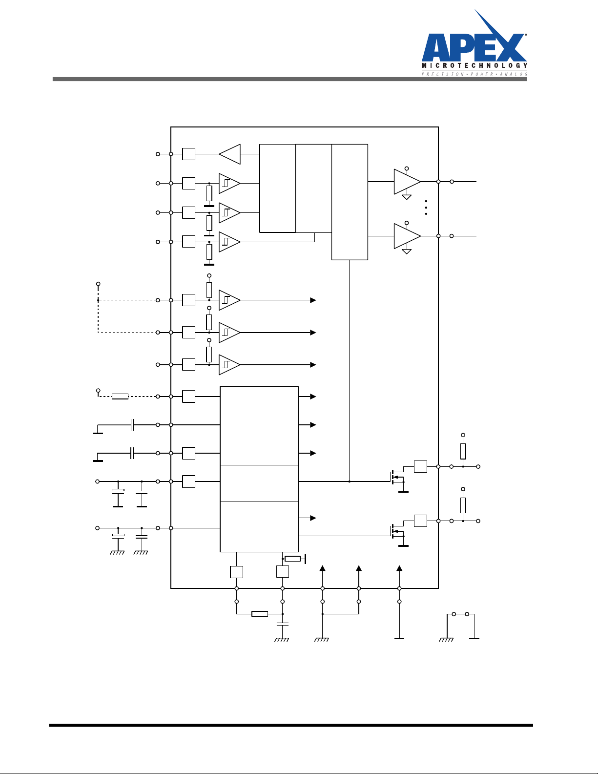
BLOCK DIAGRAM
Figure 2: Block Diagram
Power supply
HV Driver
Overcurrent
ĞƚĞĐƟŽŶ
VPP
ESD
ESD
ESD
ESD
32 Bit
^ŚŝŌ
Register
32 Bit
Latch
Error
Logic
ESD
ESD
V
DD
V
DD
OUT
DATA
CLK
LE
HI
LO
Z
IHV
VD
CP+
VDD
ESD
ESD
ESD
Error Logic
Error Logic
HV Driver
ESD
RIHV
V
DD
C2
ESD
C3
ESD
V
DD
Undervoltage
ĞƚĞĐƟŽŶ
VDD
VPP
V
PP
V
DD
ESD
ESD
OCM OCI PGND BS DGND
V
PPI
V
PPI
R1
C1
UV
OC
D01
D32
V
PPI
32 HV Driver
-1
-1
AIC1532
AIC1532
AIC1532U Rev A 3
PINOUT AND DESCRIPTION TABLE
Pin Number Name Description
1 D01 High voltage push-pull output 01
2 D02 High voltage push-pull output 02
3 D03 High voltage push-pull output 03
4 D04 High voltage push-pull output 04
5 D05 High voltage push-pull output 05
6 D06 High voltage push-pull output 06
7 D07 High voltage push-pull output 07
8 D08 High voltage push-pull output 08
9 D09 High voltage push-pull output 09
10 D10 High voltage push-pull output 10
11 D11 High voltage push-pull output 11
12 D12 High voltage push-pull output 12
13 D13 High voltage push-pull output 13
14 D14 High voltage push-pull output 14
15 D15 High voltage push-pull output 15
16 D16 High voltage push-pull output 16
17 NC not connected
18 OCI Input of the over current detection logic
19 NC not connected
20 OCM Output of the over current detection measurement circuit
21 NC not connected
22 VPP Power supply of the 32 high voltage push-pull outputs
23 NC not connected
24 NC not connected
25 DGND Digital ground. Both DGND Pins must be connected together.
26 NC not connected
27 PGND Power ground of the 32 high voltage push-pull outputs. PGND must be externally
connected to DGND, but avoid creating ground loops.
28 NC not connected
29 NC not connected
30 OC Status output of the over current detection
31 NC not connected
32 BS Backside of the chip
33 D17 High voltage push-pull output 17
34 D18 High voltage push-pull output 18

AIC1532
4 AIC1532U Rev A
35 D19 High voltage push-pull output 19
36 D20 High voltage push-pull output 20
37 D21 High voltage push-pull output 21
38 D22 High voltage push-pull output 22
39 D23 High voltage push-pull output 23
40 D24 High voltage push-pull output 24
41 D25 High voltage push-pull output 25
42 D26 High voltage push-pull output 26
43 D27 High voltage push-pull output 27
44 D28 High voltage push-pull output 28
45 D29 High voltage push-pull output 29
46 D30 High voltage push-pull output 30
47 D31 High voltage push-pull output 31
48 D32 High voltage push-pull output 32
49 ZInput to switch off all the lower and the upper transistors of the high voltage push-
pull outputs (high impedance status)
50 NC not connected
51 HI Input to switch all the high voltage push-pull outputs in the high state
52 LO Input to switch all the high voltage push-pull outputs in the low state
53 LE Input to set the 32 latches and reset the flip-flop of the over current signal
54 CLK Input to clock the shift register
55 DATA Data input of the shift register
56 IHV Input to connect an external resistor to adjust the switching speed of the high volt-
age push-pull outputs. If not used, pin must be connect to DGND
57 DGND Digital ground. Both DGND Pins must be connected together
58 UV Status output of the under voltage detection
59 CP+ Connection for the external low-pass capacitor of the under voltage detection
60 OUT Output to the cascading the IC for the next DATA Pin
61 VDD Power supply for the digital logic
62 NC not connected
63 VD Gate voltage - block capacitor for the internal driver voltage of the output stages
(without any external load)
64 NC not connected

AIC1532
AIC1532U Rev A 5
SPECIFICATIONS
Unless otherwise noted: TAMB = 25°C, high voltage supply VPP = 190 V, logic supply VDD= 5 V, IHV con-
nected to DGND.
ABSOLUTE MAXIMUM RATINGS
Parameter Symbol Min Max Unit
High voltage supply VPP VDD 280 V
Output voltage of the high voltage push-pull
outputs VDN -0.3 280 V
Logic supply voltage VDD -0.3 7 V
Slew rate of VPP 160 V/ms
Logic input levels VIN -0.3 VDD+0.3 V
Logic output levels VO-0.3 VDD+0.3 V
Output currents of the status outputs (under-
voltage and over-current detection) IO6 mA
Gate voltage VD-0.3 13 V
ESD – protection 1
1. See Figure 2 for details on which pins are ESD protected
VESD -2000 +2000 V
Continuous total power dissipation PTOT 750 mW
Storage temperature range TSTG -55 150 °C
Junction temperature range TJ-25 150 °C
Thermal resistance RTHJA 70 K/W

AIC1532
6 AIC1532U Rev A
NORMAL OPERATING RANGE
DC CHARACTERISTICS
Parameter Symbol Min Typ Max Units
High voltage supply VPP 30 190 230 V
Logic supply voltage VDD 4.5 5.0 5.5 V
Slew rate of VPP 1
1. During a data latch sequence VPP must be stable.
100 V/ms
High level input voltage VINH 2.0 VDD V
Low level input voltage VINL 0 0.8 V
Input voltage OCI On VOCIE 2.5 VDD V
Input voltage OCI Off VOCIA 0 2.0 V
Operating junction temperature TJ0 125 °C
Operating temperature TAMB 0 70 °C
Parameter Symbol Test Conditions Min Typ Max Units
Quiescent supply current of the push-
pull outputs IPPQ
VIN = 0.1 V at HI, DATA,
CLK, LE; VIN = VDD-0.5 V at
LO, Z
0.15 0.60 mA
Supply current of the push-pull out-
puts by D01 – D32 = Low IPP,ON
VIN = 0.1 V at LO, DATA,
CLK, LE; VIN = VDD-0.5 V at
HI, Z
0.50 1.00 mA
Quiescent supply current
of the logic IDDQ
VIN = 0.1 V at DATA, CLK,
LE; VIN = VDD-0.5 V at HI,
LO, Z
0.15 0.30 mA
Supply current of the logic IDD
fCLK = 2 MHz;
fData = 1 MHz 0.50 5.00 mA
High level input current at HI, LO, Z -IIN,H VIN,H = VDD-0.5 V 30 µA
Low level input current at HI, LO, Z -IIN,L VIN,L = 0.1 V 200 µA
High level input current at DATA,
CLOCK, LE IIN,H VIN,H = VDD-0.5 V 100 µA
Low level input current at DATA,
CLOCK, LE IIN,L VIN,L = 0.1V 10 µA
High level input current at OCI IOCI,H VOCI,H = VDD-0.5 V 30 µA
Low level input current at OCI IOCI,L VOCI,L = 0.1 V 10 µA
Low level output for OUT, OCM VOUT,L IOUT = 100 µA 0.5 V
High level output for OUT, OCM VOUT,H -IOUT = 100 µA VDD-1 V
Low level output for OC, UV VO,L ID = 5mA, VDD = 2.9 V 1 V
Switching level of the over current
detection at VPP IVPPU
Measured to toggle at
High on OCM;
VOCI = 0.1 V
2 5 mA
AIC1532
AIC1532U Rev A 7
Under voltage level (down) VUV- 3 3.4 3.8 V
Under voltage level (up) VUV+ 3.4 3.9 4.4 V
Residual current of one upper output
transistor -IR,OT VDS = 190 V; VIN = VDD;
VZ = 0 V
10 µA
Residual current of one lower output
transistor IR,UT 10 µA
Voltage drop over one upper output
transistor VD,OT
ID = 6.5 mA; VOCI = 0.1 V
6.5 10 V
Voltage drop over one lower output
transistor VD,UT 2.5 10 V
Minimal output current of one upper
output transistor -IDmin,OT
VDS = 30 V; VOCI = 0.1 V
20 mA
Minimal output current of one lower
output transistor IDmin,UT 20 mA
AIC1532
8 AIC1532U Rev A
AC CHARACTERISTICS
See also section SWITCHING WAVEFORMS for illustration
Parameter Symbol Test Conditions Min Typ Max Units
Clock frequency fCLK 2 MHz
Clock width high tWH 100 ns
Clock width low tWL 100 ns
Data setup time before clock rises 1
1. Data setup only during in the low phase of clock
tSU 30 ns
Delay time clock to OUT tDOUT 40 ns
Data hold time before clock rises tHCL = 20pF (Lab) or 2
2. Principle measurement of rise and fall time of D01 - D32 with test measurement unit (TMU):
50 tWH /2 ns
LE delay time after rising edge of clock tDLE 10 ns
Width of latch enable pulse tWLE 50 ns
Rise- and fall time of D01 - D32 tON, tOFF 75 µs
Trigger points TMU:
Low = 0.47 V (у19V)
High = 4.23 V (у171V)
VPP
190V
100k
2.54k
AIC1532
уϮϬƉ&
Timer Measurement
Unit (TMU)
Ri уϮϬŬɏ
-1

AIC1532
AIC1532U Rev A 9
SWITCHING WAVEFORMS
OPERATING FUNCTION TABLE
Function Inputs 1
1. L = low, H = high, X = irrelevant, = low to high transition
Outputs 2
2. L = low, H = high, Z = high impedance, * = dependent from previous CLK or LE status. OCI has the highest priority.
CLK DATA LE LO HI Z OCI OUT D OC UV
LO Mode X X X L H H L * L H H
HI Mode X X X H L H L * H H H
Z Mode X X X X X L L * Z H H
Load SR X L H H H L * * H H
Store X X H H H L * * H H
Transparent Latch L H H H H L * L H H
Mode HHHHH L *HHH
Over Current OCI X X X X X X H * L L H
C
<
DATA INPUT
CLOCK
50%
50% 50% 50%
50%
t
SU
t
H
V
IN,H
V
IN,L
V
IN,H
V
IN,L
V
OUT,H
V
OUT,L
V
IN,H
V
IN,L
V
O,H
V
O,L
V
O,H
V
O,L
DATA OUT
LATCH ENABLE
(INPUT)
LATCH ENABLE
(OUTPUT)
D01 - D32
50%
50%
50%
90%
10%
10%
t
WL
t
WH
t
DOUT
t
DLE
t
WLE
t
OFF
t
ON
90%
AIC1532
10 AIC1532U Rev A
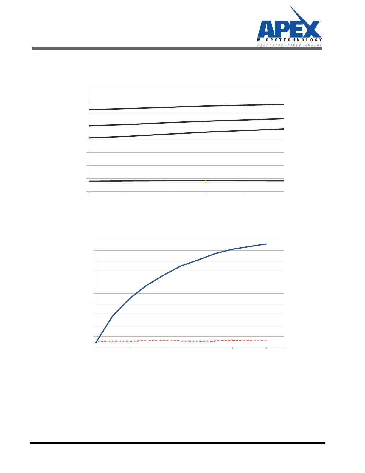
TYPICAL PERFORMANCE GRAPHS
Figure 3: Dependency of TON, TOFF from ambient Temperature
Figure 4: Dependency of TON, TOFF from IHV Resistance
Switching Time [ʅs]
max TON
40
35
30
25
20
15
10
5
0
typ TON
min TON
TAMB [°C]
0 25 50 75 100 125
max TOFF
min TOFF
Rise/Fall Time [ʅs]
20
18
16
14
12
10
8
6
4
2
0
0 200k 400k 600k 800k 1M
RIHV [ɏ]
TOFF,TYP
TON,TYP

AIC1532
AIC1532U Rev A 11
APPLICATION
Figure 5: Example Application Circuit
OVER-CURRENT DETECTION
AIC1532 includes an over-current detection circuit of the voltage supply of the high voltage push-pull out-
puts. The signal of the over-current detection can delayed or noise filtered by an external R-C combination.
AIC1532 provides an over-current measuring output (OCM) and an over-current input (OCI) signal. By activa-
tion of the over-current input (OCI) a flip-flop will be set, switching the high voltage push-pull outputs to the
low state. The over-current flip-flop can be reset by applying the latch enable signal (LE). To display the over
current a status output (OC) exist according to the logic table. It is possible to connect this output parallel
with other (OC) outputs (wired or).
UNDER-VOLTAGE DETECTION
If the logic voltage supply falls below a threshold of about 4 V, the under-voltage detection will be acti-
vated and the transistors of the high voltage push-pull outputs turns off. To display an under-voltage condi-
tion, an output (UV) is activated (pulled to low), indicating that the logic voltage supply is to small for a secure
function of the internal logic. It is possible to connect this output parallel with other (UV) outputs (wired or).
The capacitor on (CP+) serve as a noise filter capacitance for the under-voltage detection.
OTHER FUNCTIONS
The high voltage push-pull outputs are protected against a possible latch-up by using the drain diodes of
the output high voltage transistors and their complete dielectric isolation.
RS
piezo element
D0
...
D32
OUT
UV
OC
DGND
PGND
BS
OCM
to DATA of
next AIC1532
RS
piezo element
VDD
VDD
100 nF 1 nF
100 nF
4.7 ʅF/
25 V
VPP
10 ʅF/
350 V
100 nF/
400V
CONTROLLER
CLK
DATA
LE
HI
LO
Z
IHV
VD
CP+
VDD
VPP
OCI
AIC1532
RV
RV
ocm
uv
oc
oci

AIC1532
12 AIC1532U Rev A
The switching speed of the high voltage push-pull outputs is adjustable by adding an external resistance
RIHV between pin (IHV) and the logic voltage supply (VDD). If no speed adjustment is desired, the pin (IHV)
must be connected to the digital ground (DGND).
AIC1532 includes an interval power supply for the high voltage push-pull driver, requiring an external sta-
bilization capacitor connected to pin (VD). To ensure reliable operation, pin (VD) must not be connected to
any external loads.
All inputs and the low voltage outputs are protected against electrostatic discharge (ESD) up to ± 2000 V.
LIMITATIONS FOR THE LOAD SERIES RESISTOR AND THE LOAD CAPACITANCE
To protect AIC1513 against thermal over-stress, the series resistor to the connected load (RS) and the
capacitance of the connected load (CS) need to meet the following two criteria:
and
NOISE OR DELAY FILTER FOR OVER-CURRENT PROTECTION
The time constant for a noise or delay filter for the over-current protection must be set to less than 5 ms
(see Figure 2 for illustration of placement for R1 and C1):
RS
VPP
10mA
--------------
CS
5ms
RS
----------
R1C15ms=
AIC1532
AIC1532U Rev A 13
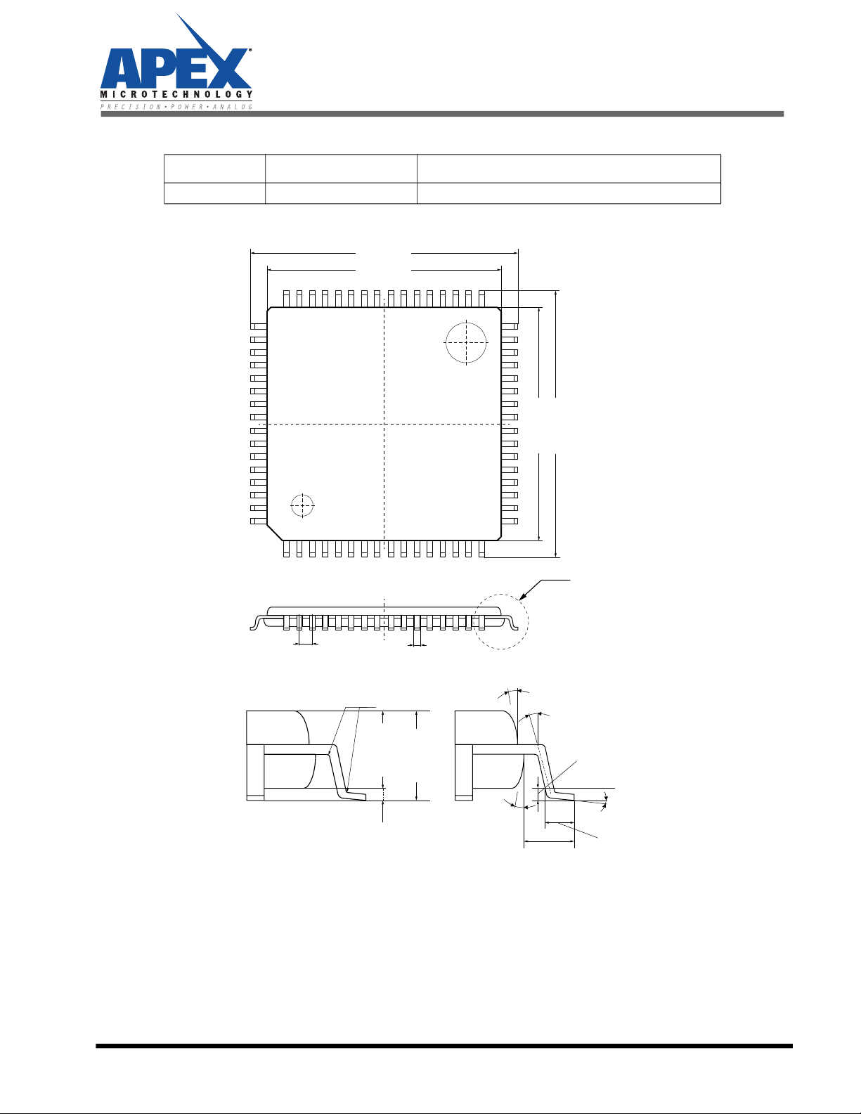
PACKAGE OPTIONS
Part Number Apex Package Style Description
AIC1532 ZD 64-pin LQFP
0.55 [14.0]
48
49
0.63 [16.0]
33
32
17
16
1
64
0.55 [14.0]
0.63 [16.0]
Detail
0.0315 [0.8] 0.0118-0.0157
[0.3-0.4]
11-13°
min 0°
0.0984 [0.25]
11-13°
0-7°
0.0393
[1.0]
0.0236±0.0059
[0.6±0.15]
max 0.063
[1.60]
0.053-0.057
[1.35-1.45]
0.0031 [0.8]
0.002-0.006
[0.05-0.15]

AIC1532
14 AIC1532U Rev A
NEED TECHNICAL HELP? CONTACT APEX SUPPORT!
For all Apex Microtechnology product questions and inquiries, call toll free 800-546-2739 in North America. For
inquiries via email, please contact apex.support@apexanalog.com. International customers can also request
support by contacting their local Apex Microtechnology Sales Representative. To find the one nearest to you,
go to www.apexanalog.com
IMPORTANT NOTICE
Apex Microtechnology, Inc. has made every effort to insure the accuracy of the content contained in this document. However, the information is
subject to change without notice and is provided "AS IS" without warranty of any kind (expressed or implied). Apex Microtechnology reserves the right
to make changes without further notice to any specifications or products mentioned herein to improve reliability. This document is the property of
Apex Microtechnology and by furnishing this information, Apex Microtechnology grants no license, expressed or implied under any patents, mask
work rights, copyrights, trademarks, trade secrets or other intellectual property rights. Apex Microtechnology owns the copyrights associated with the
information contained herein and gives consent for copies to be made of the information only for use within your organization with respect to Apex
Microtechnology integrated circuits or other products of Apex Microtechnology. This consent does not extend to other copying such as copying for
general distribution, advertising or promotional purposes, or for creating any work for resale.
APEX MICROTECHNOLOGY PRODUCTS ARE NOT DESIGNED, AUTHORIZED OR WARRANTED TO BE SUITABLE FOR USE IN PRODUCTS USED FOR LIFE
SUPPORT, AUTOMOTIVE SAFETY, SECURITY DEVICES, OR OTHER CRITICAL APPLICATIONS. PRODUCTS IN SUCH APPLICATIONS ARE UNDERSTOOD TO BE
FULLY AT THE CUSTOMER OR THE CUSTOMER’S RISK.
Apex Microtechnology, Apex and Apex Precision Power are trademarks of Apex Microtechnology, Inc. All other corporate names noted herein may be
trademarks of their respective holders.
ESD PROTECTION
The Requirements for Handling Electrostatic Discharge Sensitive Devices are described in the JEDEC stan-
dard JESD625-A. Please note the following recommendations:
• When handling the device, operators must be grounded by wearing a for the purpose designed grounded
wrist strap with at least 1M? resistance and direct skin contact.
• Operators must at all times wear ESD protective shoes or the area should be surrounded by for ESD pro-
tection intended floor mats.
• Opening of the protective ESD package that the device is delivered in must only occur at a properly
equipped ESD workbench. The tape with which the package is held together must be cut with a sharp cut-
ting tool, never pulled or ripped off.
• Any unnecessary contact with the device or any unprotected conductive points should be avoided.
• Work only with qualified and grounded tools, measuring equipment, casing and workbenches.
• Outside properly protected ESD-areas the device or any electronic assembly that it may be part of should
always be transported in EGB/ESD shielded packaging.
STORAGE CONDITIONS
The AIC1532 meets moisture sensitivity classification MSL2, according to JEDEC standard J-STD-020, and
should be handled and stored according to J-STD-033.
Table of contents
Popular DC Drive manuals by other brands


KEBCO
KEBCO COMBIVERT F5 instruction manual

American Control Electronics
American Control Electronics Minarik MDVF03-D230-PCM quick start guide

Danfoss
Danfoss FC 100 Series Programming guide

Smartrise
Smartrise DSD412 Startup manual

Minarik
Minarik RG501A user manual

Rockwell Automation
Rockwell Automation RELIANCE ELECTRIC DC3N Series user guide

Pfeiffer Vacuum
Pfeiffer Vacuum TCP 380 operating instructions

Siemens
Siemens SINAMICS GL150 Operating and installation instructions

Cole Parmer
Cole Parmer Masterflex 7583-50 operating manual

Parker
Parker E-DC Quick reference guide

Rockwell Automation
Rockwell Automation PowerFlex 40 quick start guide

EACON
EACON EC620 quick guide