Arcam DiVA DV78 User manual

DiVA Service
Manual
DV78 DVD Player
Issue 1.0
ARCAM
Bringing music & movies to life

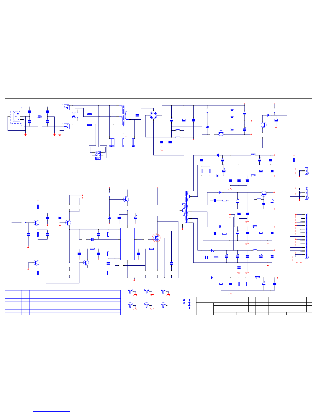
Circuit Description
Power Supply L959AY
! CCT diagram
! Component layout diagram
! Parts list
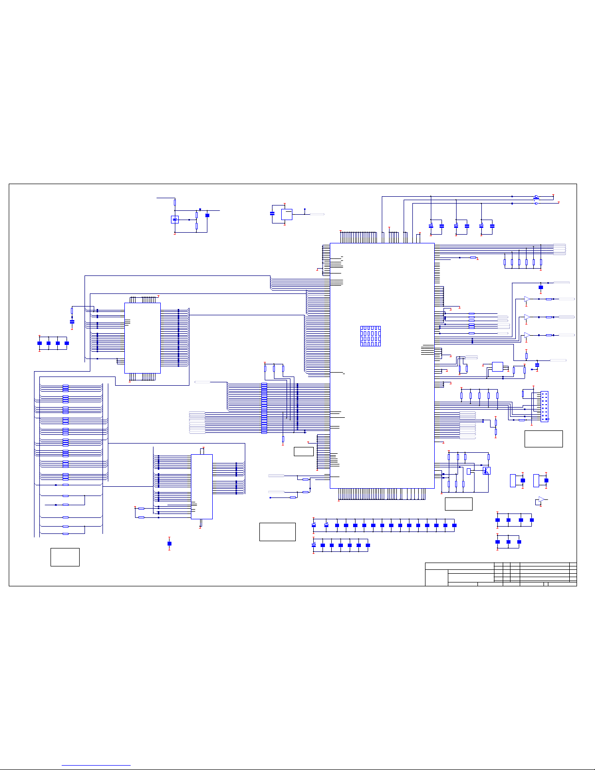
Main Board L960AY
! CCT diagram
! Component layout diagram
! Parts list
Display Board L961AY
! CCT diagram
! Component layout diagram
! Parts list
Transformers
! L924TX
! L925TX
Mechanical Assembly
! Exploded view diagram
! Mechanical and packing part list
DV78
Contents List

Overview
The DiVa DV78 is a completely new design platform
that share a similar circuit topology to the earlier
released Vaddis V based players such as the Diva
88+, Diva 89, DV27.
The player is based around acclaimed Zoran Vaddis
Vchipset coupled to high specification Wolfson D to A
converters for Left and Right channels.
Power supply board.
Non-switching
Mains power arrives at IEC inlet socket SKT1 and is
filtered by EMC choke LI and Y caps C3 and C4,
mains switch SW2a/b switches both Negative and Live
phases before the power reaches the mains select
switch at location SW1 the switch allows the primary
windings of the transformer TX1 to be wired in either
Parallel or Series configuration.
The Bridge rectifying Diode package at location D1
forms the basis of the conventional power stage and
supplies a VN35V6 (-35.6v) to the Switch mode
stage, transistor TR1 is biased by 2v7 Zener diode
DZ1 and allows for the series Zener diodes DZ2, DZ3,
DZ3 to supply the VN13V5 and VN19V rails.
We will also see a simple A.C present circuit this is
used for delayed output relay operation and fast relay
closure under interrupted supply conditions thus
preventing op-amp offsets from reaching the Audio
output sockets.
Switch mode
The switch mode supply is formed around the
Driver/Control chip IC1 UC3843 (used in regulating
mode). The chip is referenced the –36.5V supply line
and the Digital ground DGND, the supply for the chip
is formed by the 12v Zener at location DZ6 and can be
seen on Pin 7 as VCC. The power supply allows for
the switch-mode to be tied the to Audio sampling
frequency for any given compatible format.
Fig 1 PSU clock control
Fs
Frequency
select
PSUFS1
Pin 11
IC305a
PSUFS0
Pin 12
IC305a
PSUCLK
Output Pin 5
of IC305a
44.1 kHz 0 0 44.1 kHz
48 kHz 0 0 48 kHz
88.2 kHz 0 1 44.1kHz
96 kHz 0 1 48 kHz
176.4 kHz 1 0 44.1 kHz
192 kHz 1 0 48 kHz
Others 1 1 OFF
The PSU sync signal is driven into the power supply via
Resistor R9 if no Sync is present the unit is set to free run x
due to the RT/RC network attached to Pin 4.
IC1 is running in regulated mode and monitors the voltage
output on the +5V and +3V3 D.C lines, the two voltages are
summed by TR8 and Driven into the VFB and Comp inputs
of IC1, the Voltage is then regulated by changing the time
base of the PWM output at pin 6 (longer the time base the
lower the voltage), the PWM switching frequency is driven
into the switch-mode transformer by the high speed Nmos
device at position M1, R5 is used to sense the Current
across the gate of the Nmosfet and in the event of a short
circuit will safely shut the power supply down. We derive the
12v Mech supply from the output of M1 using the Ultra-fast
Diode at location D8 to rectify the PWM line.
The D.C outputs from the switch mode have extensive
switch mode noise removing filters these are seen as 100n
caps down to ground and Wire wound inductors in series
with the supply rail.
Power supply main board
All the power supply rails are supplied to the main board via
the 32 way FFC connector at location CON1001.
The Digital supplies from the switch mode stage of the
power supply arrive as 3V3D, +5VD and +12VD we also see
the Display board power supplies arrive as –19V, -9 and
–13.5V all of the supplies have a second stage of
implemented on the board to remove all traces of ultra-sonic
noise.
The 3V3D rail is the main 3V3 rail used to power the digital
circuitry; +5VD is used for all 5v Digital/Video supplies the
+12VD is used for Scart switching.
Diva Dv78 circuit description

The 1V8 rail is derived from the 3V3 rail and is
regulated by the adjustable regulator at location
REG1003.
The Analogue supply stages arrive at the main board
as +15V3 and –15V3 rails these are filtered L1002 and
L1015 before being regulated by the adjustable
regulators at locations REG1000 and REG1002 to
provide +/- 12V rails for the Analogue output stage.
Regulator REG1001 is fed from the +15V3 rail and
forms the Audio DAC supply.
The Display board requires several supply voltages
these are simply passed through the main board,
being filtered on the way to prevent transmission of
noise through to the surrounding electronics. The
display takes the +5V, -19V, -13V5 and -9V the –13V5
and –9V form a floating 4.5V supply biased relative to
the –19V grid voltage.
Display Board
The main component of the Display board is IC1 this is
a Vacuum Florescent Display driver with keyboard san
and a serial data in/out interface.
The Chip receives display drive serial data from the
Vaddis V chip on the main board via Con1 on pins 12,
13 and 14 these will be seen a DIN, STS and CLK this
data is used to drive the VFD a DOUT line interfaces
with the VADDIS V and supplies Keyboard Scan
information. The keyboard scan is a 6 x 4 matrix with
the Key Source appearing at S3, S4, S5, S6 and the
Keyscan data returns appearing a K2, K3 and K4.
Please see: above for power supply information.
The Infra red pick-up at location RXI receives RC5
data and send the data to the Vaddis V on the main
board via transistors TR2 and TR3, LED 2 is used to
mix the rear panel RC5.
The rear panel 3.5mm input jack receives modulated
RC5 code; this is filtered for ultra sonic noise by the
inductors at locations L900 and L901 and then passed
to the Infrared diode on the display at location LED2.
Main Board electronics DV78.
Zoran Vaddis V.
The main processor/control chip on the main board is the
Zoran Vaddis V at location IC202, this is the latest
incarnation of the very popular Vaddis range of processors
and allows for a much lower component count when
compared to our earlier players as many of the playback
functions have moved onto the Vaddis V silicon.
Below you will see the major functions of the Vaddis V
when used with the DV78.
o Decoded Analogue Video output (internal
DAC) used on the DV78 only.
o SPDIF output.
o Internal display interface.
o Internal ATAPI interface.
o Internal IR interface.
o Serial in/out for RS232 (Optional).
A more detailed explanation of the Vaddis V and
peripheral components follows.
Vaddis Power
The Vaddis V is powered by two separate supplies the
Vaddis requires a 1.8v supply for the core, this is regulated
from the 3.3v rail by REG1003, the 3.3v rail is used to
supply power to the I/P – O/P ports of the chip.
ATAPI interface
CON203 is an ATAPI interface on a 40 way IDE
connector. This is decoupled from the Drive via an array of
decoupling resistors as required by the ATAPI spec.

Display Board interface
The display board interface is on the 16 way FFC flexi
foil connector at location CON202. Power for the
display also travels on the connector. There are 4 –
wires to interface with the VFD driver chip these are
seen as.
o XFPDIN - Data to the display board
o FPDOUT - Data from the display board
o XFPCLK - Clock
o XFPSEL - Chip select
The above control lines are level shifted to 5v logic
from 3.3v levels by IC200 (74HCT125) these are the
levels required by the VFD drive chip.
The IR output from the Display board arrives as
IRRCV this is an open collector signal, which can be
wire-Ord with the re-panel remote input.
Digital Audio
The Digital audio leaves the chip as 1 data line
labelled as.
o ADAT0 - Left and Right channel data
Along with the ADAT line we will also see the ABCLK
and ALRCK as required for IS2 data conversion.
The Vaddis V also supplies a direct SPDIF output for
interfacing with ancillary processing equipment.
Flash/ SDRAM
IC203 is a 64Mbit (32 bit x 2Meg) SDRAM. It runs at
135MHz
IC205 is a 16Mbit (16 bit x 1Meg) intel type flash IC for
program storage (Player software).
The flash interfaces to the Vaddis V using the SDRAM
bus it may appear that the bus connects to the flash in
a random manner, however this is simply because the
Vaddis bus is multiplexed that way. The Flash will be
accessed at power up and the contents are copied to
the SDRAM the program will then be run from the
SDRAM.
Series resistors are employed to isolate the flash bus
from the main SDRAM bus.
EEPROM
IC204 is a 8kBit (1K x 8) Serial EEPROM. This is used
for storage of non-volatile storage of player settings,
region settings and bookmark data.
Clocks
CLK27MV is the 27Mhz clock for video. It is used to
generate the 135Mhz clock for the Vaddis microprocessor
and DSP. The MCLKV is the audio master clock for the
Vaddis.
We run the Vaddis in PLL bypass mode and generate or
own master clock (see main clock section of manual) for
higher accuracy and improved performance across Audio
and Video.
RESET
IC201 is a reset generator chip that monitors the +3.3V rail
and ensures a reset signal PWR_ON_RESET* is
generated on power up, or if the mains power dips below
an operational level.
This signal is used to reset the Vaddis V and Flash micro
only. The Vaddis V line labelled as RESET* resets the
remaining circuitry of the player apart from the HDMI chip,
this has it’s own reset line labelled as HDMI_RESET this is
necessary if we require to reset the HDMI chip only (for
example when the HDMI sink is connected and then
disconnected).
Serial Port
The VADDIS V can interface with the external world via
the RS232 connector at location CON900 and the RS232
Transceiver at location IC900, the serial data lines are
shown as SERIAL RX and SERIAL TX these lines allow
for direct control over the unit via RS232.
Fig 2. GPIO control signals from the Vaddis V
Single Name I/P-O/P
Function
PSUFSO-1 Output
Control PSU Clock
divider
ENABLE_AV Output
SCART control High
in normal operation
and low in standby
16/9 Output
Scart 16/9
anamorphic control
line
GAIN_SCALING Output
High for HDCD gain
scaling
ML_8740_0-2 Output
SPI load signal for
Audio DACs 0
MC Output
SPI clock signal for
DAC control
MD Output
SPI data signal for
DAC control
FSELE0-1 Output
Frequency select
generator
MUTE* Output
Active low audio
mute signal
RESET* Output
System reset

Clocks and SPDIF stage.
IC300 is a PLL1700E clock generator IC the chip is
powered from the +5V(D) rail. The Chip runs in
software mode and is slaved from the Vaddis V (data
coming in on the MD line).
X300 is a 27Mhz crystal that IC300 uses to generate
all the video and audio clocks required by the system
the crystal sits on the XTI and XTO pins of the chip,
the 27Mhz output at Pin 10 (MCKO) is used to drive
the Vaddis chip directly bypassing the internal PLL.
The frequency of the audio master is dependent on
the on the current audio sample rate (I.e the sample
rate required by the format CD=44.1Khz and
DVD=48khz etc) and this is set by the system micro
via the MD, MC and ML_1700 lines from the Vaddis V.
Clock Buffer
IC301 us used to buffer the audio master clock. The
circuit is arranged so that each device that requires
the audio master clock has it’s own driver these are
seen as.
o MCLK_DAC0 - Pin 18
o MCLK_DAC1 – Pin 16
o MCLK_DAC2 – Pin 14
o MCLK_VADDIS – Pin 3
o MCLK_HDMI – Pin 9
We also run the Mute Line from the Vaddis V IC301
this can be seen on Pin 12 and drives transistor
TR401, the transistor pulls the relays RLY400,
RLY500, RLY600 to ground and un-mutes the audio
outputs.
IS2 Audio Data
IC302 and IC309 are buffers for the 12S signals these
ensure that the signals travelling to the DAC’s are
point to point. IC302 deals with the ALRCK and
ABCLK and IC309(NF DV78) the
ADAT0,1,2 all signal are split into three separate lines
for the three stereo DACS.
PSU Clock Divider
IC304 a/b form a clock divide by 1, 2 or 4 to ensure
the PSU clock is always either 44.1kHz or 48Khz (See
fig 1 within the power supply description section).
The circuit is fed from the ALRCLK (Audio clock) the
selected PSUCLK is controlled by PSUFSO and
PSUFS1.
The output of the PSU circuit can be seen to leave
IC305 on pin 5 via R311. Please see Fig 1 for PSU
control information.
The circuit will also switch the PSUCLK off when switching
between sample rates (the PSU will free run when the
PSUCLK is not present).
SPDIF Output
The SPDIF output consists of IC901 implemented as a
inline buffer and parallel output buffer. Gate A buffers the
signal so that the SPDIF line from the VADDIS sees fewer
loads and form a feed to the Optical output transmitter,
gates B,C and D drive the SPDIF in parallel so that we can
drive a 75ohm load adequately. The resistors at the output
of IC901 are arrange so that the output will be 500mV pk-
pk when the output is terminated with a 75 ohm load at the
same time the output impedance of the circuit is 75ohms
as required by the Sony Philips Digital Interface
specification.
Left and Right channel D to A stages
The Wolfson WM8740 stereo DAC ay location IC403
requires +5V(A) and a +3V3 supply along with the Digital
Audio data lines already described in this guide.
The Left channel output only will be described in this
section.
IC400B and associated components form a 2
nd
order
Bessel filter with a differential input and a gain of 1 this
follow by a output buffer IC401B, the gain of IC401B is
control by the switching chip at location IC402, in normal
use the Gain of IC401B is set to 1.1 but in HDCD mode
the IC402 switches a second 10k resistor in parele with
R413 and the gain is set to 2.2 allowing for the higher
audio output required by the HDCD standard.
C436 is an A.C coupling capacitor used to remove the few
mV of offset that the DAC produces; D400 provides
protection against from ESD.
The all output relays are under control of the Vaddis V
chip but will also mute the outputs instantly under mains
failure conditions. Switching drive is provided by TR401
(MUTE_BUF) and TR400 (AC_PRES) the relays are in
mute mode if either the input to TR401 is Low or if the
input to TR400 is high.
Please note: The Scart left/right audio is fed from the
outputs of the left/right audio stages.

Video Output stage
The DV78 video output stage makes use of the
VADDIS V’s on board video DAC stages and as such
does not use the superior Analogue devices video
encoder DV79/DV29 and is fed by the following video
lines from the Vaddis V.
o Composite
o SVID_C
o SVID_Y
o V or Red
o U or Blue
o Y or Green
If we look at the Composite stage only, we will see that
the Analogue video signal is filtered by C710, C711
and L705 before being passed through the Video Op-
amp at location IC701 the output is decoupled by
capacitor C738 before reaching R714 this forms the
75 ohm load required. All other video outputs are
identical.
SCART Output
RGB and Composite video signals as well as Left and
right audio signals are all present on the SCART
output socket. As the RGB and YUV signals share the
same output port at the Vaddis V the player must be
set to RGB SCART operation to have a RGB output
on the SCART.
Please note: When in RGB SCART mode the RGB
does not contain a Sync signal and the sync must be
taken from the Composite out (4 wire RGB).
Also present at the Scart are a number of control flags
for the monitor these include 2 GPIO control lines
direct from the Vaddis.
o ENABLE_AV
o 16/9
These are seen at the SCART output pins as.
o O/6/12
o RGB STAT
The 0/6/12 line (SCART pin 8) is used to inform the
monitor of the screen format being sent by the player
as set in the video set-up section of the software.
o Standby = 0V
o 16:9 aspect ratio = 6V
o 4:3 aspect ration = 12V
The RGB status line (SCART pin 16) will be seen as
0v = no RGB and >1v is RGB present.
ISSUE
DRAWING NO.
DRAWING TITLE
DATE
Filename:
ECONo. DESCRIPTION OF CHANGE
L959_1.1.sch
DV78 SERIES PSU
Contact Engineer:
L959CT
22 Apr 2004
INITIALS
Printed:
1 1Sheet of
Notes:
Contact Tel: (01223) 203200Kevin Lamb
A & R Cambridge Ltd.
Pembroke Avenue
Cambridge CB5 9PB
Waterbeach
DGND
DGND
DGND
DGND
DGND
VN35V6
VN35V6 VN35V6VN35V6
DGND
115V
115V
6
4
2
1
5
3
7
TX1
Small Toroidal Mains
L924TX
D1
2KBP02
VN35V6
DGND
1
2
3
4
5
6
CON1
MOLEX
44472
L
N
E
SKT1
BULGIN
PX0580
C2
C1 C3
3N3
250V
CER
C4
3N3
250V
CER
1
3
4
2
L1
250U
SW2A
SDDFC30400
SW2B
SDDFC30400
1A
1
1B
2A
2
2B
115V 230V
SW1
18-000-0019
FHLDR2
20mm HLDR
FHLDR1
20mm HLDR
FS1 T315mA
S504
FS2
T315mA
S504
VN19V
EMC Shield
SH1
1
2
3
4
CON5
Amp
HD Pwr Con
VP5V
VP12V
DGND
1
2
3
4
5
6
7
8
9
10
11
12
13
14
15
16
17
18
19
20
21
22
23
24
25
26
27
28
29
30
31
32
CON7
MOLEX
52045
VN19V
VN13V5_F1
VN9V_F2
DGNDAGND
VP12V
VP15V5
VP5V
VP3V3
VP3V3
VN15V5
VP5V
VP3V3
VP3V3
VP3V3
VP3V3
VP5V
SPARE3
SPARE4
AC_PRES*
PSU_CLK
DGND
VP3V3
VP5V
SPARE1
SPARE2
C46
470UF
25V
YK
C39
220UF
16V
YXF
C54
1000UF
16V
YXF
C55
1000UF
16V
YXF
C45
470UF
25V
YK
C44
470UF
25V
YK
D4
UF4003
DO-41
C34
1N0 100V
CER
C36
1N0
100V
CER C25
100N
100V
MKS2
C20
100N
100V
MKS2
C22
100N
100V
MKS2
C21
100N
100V
MKS2
C23
100N
100V
MKS2
C26
100N
100V
MKS2
C24
100N
100V
MKS2
C19
100N
100V
MKS2
C18
100N
100V
MKS2
R31
10R
0W25
MF
R18
10R 0W25
MF
R22
470R 0W25
MF DZ5
BZX79C
5V1
DO 35
TR6
BD179
TO-126
R24
33R 0W25
MF
R5
4K7 0W25
MF
C40
220UF
16V
YXF
C17
100N
100V
MKS2
DZ6
BZX79C
12V
DO-35
R11
9K1
0W25
MF
R7
6K8
0W25
MF
R4
4K7 0W25
MF
R26
68R
0W25
MF
R27
2K7
0W25
MF
R25
100R
0W25
MF
R28
22R
0W25
MF
R15
10K
0W25
MF
C50
22N 100V
MKS2
C16
100N
100V
MKS2
C56
4N7
100V
CER
TR8
BC556B
TO-92
M1
IRF640N
TO-220
C6
100N
100V
MKS2
C7
100N
100V
MKS2
COMP
1
VFB
2
ISEN 3
RT/CT
4
GND
5
OUT 6
VCC 7
VREF
8
IC1
UC3843AN
DIP-8
TR7
BC556B
TO-92
DGND
TR3
BC546B
TO-92
R13
10K
0W25
MF
VP5V
PSU CLK
C35
1N0 100V
CER
R19
10R 0W25
MF
C33
1N0 100V
CER
R23
33R 0W25
MF
AGND
C41
470UF
25V
YK
C9
100N
100V
MKS2
C10
100N
100V
MKS2
C12
100N
100V
MKS2
R20
470R
0W25
MF
D2
UF4003
DO-41
C42
470UF
25V
YK
C13
100N
100V
MKS2
D3
UF4003
DO-41 C11
100N
100V
MKS2
VP15V5
VN15V5
VN13V5_F1
VN9V_F2
VP5V
VP3V3
VP12V
VN35V6
R3
4K7
0W25
MF
TR2
BC546B
TO-92
R6
6K8
0W25
MF
C31
22UF
63V
YK
VP5V
DGND
AC_PRES*
R9
1K0 0W25
MF
TR4
BC546B
TO-92
C47
22P
100V
N150
DGND
R8
1K0
0W25
MF
C14
100N
100V
MKS2
R10
1K0 0W25
MF
C15
100N
100V
MKS2
VN35V6
5V_NFB
3V3_NFB
3V3_NFB
5V_NFB
C51
22N
100V
MKS2
L6
6U8 2.1A 8RHT2
L7
6U8 2.1A 8RHT2
L5
33U 1.17A 8RHT2
L3
33U 1.17A 8RHT2
L4
33U 1.17A 8RHT2
VN35V6
VN35V6
VN13V5_F1
C29
22UF
63V
YK
MA NS SUPPLY
FOR EXT. AUDIO
SUPPLY TX
C49
22N
100V
MKS2
R14
R29
82K 0W25
MF
NF
NFB (To Controller E/A)
(NFB From PSU Outputs)
GREY 4
DK GREY 3
LT GREY 2
BLUE 1
CON2
WAGO
256
GREY 2
GREY 1
CON4
WAGO
256
GREEN 1
CON3
WAGO
256
GREY
WH TE
BLACK
BLUE
R16
47K
0W25
MF
C53
1000UF
16V
YXF
C8
100N
100V
MKS2
QTY DESCRIPTIONPART No. NOTESITEM
ITEM1 1 Clip For SW Profile HeatsinkF006
ITEM3 2 Fuseholder Cover For 20mm FuseholderF022
ITEM2 1 Sil Pad For TO-220 HS InsulatorF082
ITEM4 1 Blank PCB DV78 PSUL959PB
C37
100UF
50V
YXF
C38
100UF
50V
YXF
C57
470UF
25V
YXF
C30
22UF
63V
YK
C43
470UF
25V
YK
NF
NF
1
2
3
4
5
6
7
8
CON6
AMP
CT
NF
R32
C5
AGND
DGND
LK2
ITEM5 1 Earth Lead Assy 75MM8M101 SAFETY EARTH WIRE FROM IEC INLET SK1 TO METAL CHASSIS
L2
LK1
0R0 0W25 MF
D5
1N4148
DO 35
1
FIX2
Dia 3.5mm
1
FIX4
Dia 3.5mm
1
FIX5
Dia 3.5mm
7
2
3
16T
16T
22T
14T
10T
8
1 11
10
9
12
4
41T
41T
5
6
SCR
TX2
Ferrite Switch Mode
L925TX
DGND
FD1
FD2
TOOL1
TOOL2
TOOL3
TOOL4
C27
1000UF
63V
YK
C28
1000UF
63V
YK
C48
1N0
100V
CER
TR5
BD179
TO-126
R12
10K
0W25
MF
D6
31DQ10 DO-201AD
D7
31DQ06 DO-201AD
D8
UF5406
DO-201AD
R21
470R
0W25
MF
C32
470pF
1kV
DE
DZ4
BZX79C
5V6
DO 35
1
FIX1
Dia 3.5mm
1
FIX3
Dia 3.5mm
1
FIX6
Dia 3.5mm
NF
NF
R17
10R
0W25
MF
TR1
BC547B
TO-92
DZ1
BZX79C
2V7
DO 35
R1
22K
0W25
MF
R2
220R
0W25
MF
HS1B
SW38-2
10 2C/W
NOTE TRANSFORMER TX1 IS MOUNTED ON
THE CHASSIS AND CONNECTED TO THE PSU
PCB BY CON2,3,4. TX1 IS SHOWN ABOVE FOR
CIRCUIT OPERATION
NF
R33
1K0
0W25
MF
USED TO SECURE TRANSFORMER CABLES TO PCB NEAR CON1
NF
ITEM7 2 Rivet CopperHP007S RIVETS TO SECURE IEC INLET TO PCB
DZ2
BZX79C
10V
DO 35
DZ3
BZX79C
3V3
DO 35
NF
C52
330P
100V
N750
R30
0R22
3W
SPRX
1.0
Production release02/07/03KAL03_E195
1.1
Make CON1 fitted (used in DV29)22/04/04PG04_E046
ITEM6 1 Cable Tie 100MM X 2.5MMF044


DV78 DVD player PSU board L959AY issue 1.1.1
Designator Part Description
C1 2J410 Capacitor SM 0805 X7R Ceramic 10% 50V 100N
C2 2J410 Capacitor SM 0805 X7R Ceramic 10% 50V 100N
C3 2J410 Capacitor SM 0805 X7R Ceramic 10% 50V 100N
C4 2J410 Capacitor SM 0805 X7R Ceramic 10% 50V 100N
C5 2MA610 Capacitor Surface Mount Electrolytic 10UF 50V 6.3 X 4.5MM
C6 2MA610 Capacitor Surface Mount Electrolytic 10UF 50V 6.3 X 4.5MM
C7 2MA610 Capacitor Surface Mount Electrolytic 10UF 50V 6.3 X 4.5MM
C8 2L210 Capacitor SM 0805 NPO Ceramic 5% 100V 1N0
C9 2L210 Capacitor SM 0805 NPO Ceramic 5% 100V 1N0
C10 2L210 Capacitor SM 0805 NPO Ceramic 5% 100V 1N0
C11 2L210 Capacitor SM 0805 NPO Ceramic 5% 100V 1N0
CON1 8K8616 Con 1.0MM Horiz FFC 16WAY 52807 Series
D1 3AS16W Diode Surface Mount Small Signal BAS16W SOT-23 Package
D2 3AS16W Diode Surface Mount Small Signal BAS16W SOT-23 Package
D3 3AS16W Diode Surface Mount Small Signal BAS16W SOT-23 Package
D4 3AS16W Diode Surface Mount Small Signal BAS16W SOT-23 Package
DISP1 B1014 Display DV88
IC1 5H6312 IC VFD Driver PT6312LQ SM LQFP-44 package
LED1 3D007 LED 3.1mm Green SLR-37MG3T
LED2 3D010 LED SM Red SML-010LT
LED3 3D007 LED 3.1mm Green SLR-37MG3T
LED5 3D006 LED 3mm Red/Green Tri-Colour L-93WEGW
R1 1M133 Resistor 0805 Surface Mount 0.125W 1% 330R
R2 1M133 Resistor 0805 Surface Mount 0.125W 1% 330R
R3 1M133 Resistor 0805 Surface Mount 0.125W 1% 330R
R4 1M122 Resistor 0805 Surface Mount 0.125W 1% 220R
R5 1M118 Resistor 0805 Surface Mount 0.125W 1% 180R
R6 1M139 Resistor 0805 Surface Mount 0.125W 1% 390R
R8 1M310 Resistor 0805 Surface Mount 0.125W 1% 10K
R9 1M310 Resistor 0805 Surface Mount 0.125W 1% 10K
R10 1M247 Resistor 0805 Surface Mount 0.125W 1% 4K7
R11 1M356 Resistor 0805 Surface Mount 0.125W 1% 56K
R13 1M310 Resistor 0805 Surface Mount 0.125W 1% 10K
R14 1M310 Resistor 0805 Surface Mount 0.125W 1% 10K
R15 1M310 Resistor 0805 Surface Mount 0.125W 1% 10K
RX1 B2109 IR Receiver Module Kodenshi KSM-902TM1N
SW1 A1511 Switch Tact Low Profile No Gnd Pin
SW2 A1511 Switch Tact Low Profile No Gnd Pin
SW3 A1511 Switch Tact Low Profile No Gnd Pin
SW4 A1511 Switch Tact Low Profile No Gnd Pin
SW5 A1511 Switch Tact Low Profile No Gnd Pin
SW6 A1511 Switch Tact Low Profile No Gnd Pin
SW7 A1511 Switch Tact Low Profile No Gnd Pin
SW8 A1511 Switch Tact Low Profile No Gnd Pin
SW9 A1511 Switch Tact Low Profile No Gnd Pin
TR2 4D10KN Digital Transistor MMUN2211LT1 SOT23 Package
TR3 4A849B Transistor BC849B SOT23 Package
TR4 4A849B Transistor BC849B SOT23 Package
TR5 4D10KP Digital Transistor MMUN2111LT1 SOT23 Package

ISSUE
DRAWING NO.
DRAWING TITLE
DATE
Filename:
ECONo. DESCRIPTION OF CHANGE
L960C1_1.2.Prj
DV78 MAIN BOARD TOP LEVEL
Contact Engineer:
L960C1
2 Dec 2003
INITIALS
Printed:
1 10Sheet of
Notes:
Contact Tel: (01223) 203270PeterGaggs
A & R Cambridge Ltd.
Pembroke Avenue
Cambridge CB5 9QR
Waterbeach
A2
ATDD[0..15]
ATDMARQ
ATDIOW*
ATDIOR*
ATIORDY
ATDMACK*
ATINTRQ
ATDA0
ATDA1
ATDA2
ATCS0*
ATCS1*
MUTE*
ML_8740_0
MC
MD
ML_8740_2
ML_1700
ML_8740_1
ENABLE_AV
16/9
GA N_SCAL NG
SERIAL_RX
SERIAL_TX
IRRCV
XFPSEL
XFPCLK
XFPD N
FPDOUT
SPDIF
ADAT_DAC1
ADAT_DAC2
ADAT_DAC0
ABCLK
ALRCLK
U/BLUE
V/RED
Y/GREEN
COMPOSITE
SVID_Y
SVID_C
XATRESET*
CLK27M_VADDIS
MCLK_VADDIS
RESET*
PSUFS0
PSUFS1
VADDIS V
L960C2_1.2.sch
RESET*
ML_1700
MC
MD
CLK27M_VADDIS
MCLK_VADDIS
MCLK_DAC0
MCLK_DAC1
MCLK_DAC2
ABCLK
ALRCLK
ABCLK_DAC0
ABCLK_DAC1
ABCLK_DAC2
ALRCLK_DAC0
ALRCLK_DAC1
ALRCLK_DAC2
PSUCLK
PSUFS0
PSUFS1
MUTE*
MUTE_BUF*
CLOCKS
L960C3_1.2.Sch
ALRCLK_DAC0
ADAT_DAC0
ABCLK_DAC0
MCLK_DAC0
MD
MC
ML_8740_0
RESET*
GAIN_SCAL NG
LEFT_OUT
LEFT_OUT_GND
RIGHT_OUT
RIGHT_OUT_GND
MUTE_BUF*
AC_PRES*
SCART_LEFT
SCART_RIGHT
DAC L&R
L960C4_1.2.Sch
ALRCLK_DAC1
ADAT_DAC1
ABCLK_DAC1
MCLK_DAC1
MD
MC
ML_8740_1
RESET*
LS_OUT
LS_OUT_GND
RS_OUT
RS_OUT_GND
DAC LS&RS
L960C5_1.2.Sch
ALRCLK_DAC2
ADAT_DAC2
ABCLK_DAC2
MCLK_DAC2
MD
MC
ML_8740_2
RESET*
CENTRE_OUT
CENTRE_OUT_GND
SUB_OUT
SUB_OUT_GND
DAC CENTRE&SUB
L960C6_1.2.Sch
Y/GREEN
Y_OUT
Y_OUT_GND
SCART_GREEN
U/BLUE
U_OUT
U_OUT_GND
SCART_BLUE
V/RED
V_OUT
V_OUT_GND
SCART_RED
SVID_Y
SVID_Y_OUT
SVID_Y_OUT_GND
SVID_C
SVID_C_OUT
SVID_C_OUT_GND
COMPOSITE
COMPOSITE_OUT
COMPOSITE_OUT_GND
SCART_COMPOSITE
SVID_SCRN
VIDEO FILTERS
L960C7_1.2.Sch
SCART_LEFT
SCART_RIGHT
SCART_BLUE
SCART_GREEN
SCART_RED
SCART_COMPOSITE
ENABLE_AV
16/9
SCART
L960C8_1 2.Sch
REMOTE_BUS
REMOTE_GND
IRRCV
SPDIF
SPDIF_OUT
SPDIF_GND
SERIAL_TX
SERIAL_RX
ENABLE_AV
REMOTE_BUS_P
REMOTE_BUS_N
SPDIF & COMMS
L960C9_1.2.Sch
+5VD_ N
+3V3D_ N
+15V5_ N
-15V5_ N
-13V5_ N
-9V_OUT
-9V_ N -13V5_OUT
-19V_IN
-19V_OUT
+5V_DISPLAY
+12VD_ N
POWER
L960C10_1.2.Sch
1
2
3
4
5
6
7
8
9
10
11
12
13
14
15
16
17
18
19
20
21
22
23
24
25
26
27
28
29
30
31
32
33
34
35
36
37
38
39
40
CON100
3M
2540
ATDD[0..15]
XATRESET*
DGND
ATDD7
ATDD8
ATDD6
ATDD9
ATDD5
ATDD10
ATDD4
ATDD11
ATDD3
ATDD12
ATDD2
ATDD13
ATDD1
ATDD14
ATDD0
ATDD15
ATDMARQ
ATDIOW*
ATDIOR*
ATIORDY
ATDMACK*
AT NTRQ
ATDA1
ATDA0
ATDA2
ATCS0*
ATCS1*
DRIVE
1
2
3
4
5
6
7
8
9
10
11
12
13
14
15
16
CON101
MOLEX
52806 DGND
DISPLAY
+5V_DISPLAY
-19V_OUT
-13V5_OUT
-9V_OUT
RESET*
MD
MC
ML_1700
PSUFS0
PSUFS1
ADAT_DAC0
ADAT_DAC1
ADAT DAC2
ABCLK
ALRCLK
MUTE*
CLK27M_VADDIS
MCLK_VADDIS
MD
MC
ADAT_DAC0
ABCLK_DAC0
ALRCLK_DAC0
MCLK_DAC0
ML_8740_0
RESET*
GAIN_SCAL NG
MUTE_BUF*
ADAT_DAC1
ABCLK_DAC1
ALRCLK_DAC1
MCLK_DAC1
MD
MC
RESET*
ML_8740_1
ADAT DAC2
ABCLK_DAC2
ALRCLK_DAC2
MCLK_DAC2
MD
MC
RESET*
Y/GREEN
U/BLUE
V/RED
SVID_Y
SVID_C
COMPOSITE
Y/GREEN
U/BLUE
V/RED
SVID_Y
SVID_C
COMPOSITE
FPDOUT
XFPCLK
XFPSEL
XFPDIN
IRRCV
IRRCV
REMOTE_BUS
REMOTE_BUS_GND
REMOTE BUS
SCART_GREEN
SCART_BLUE
SCART_RED
SCART_COMPOSITE
ENABLE_AV
16/9
SERIAL_TX
SERIAL_RX
ENABLE_AV
SKT100
KUNMING
GOLD
SCART_RIGHT
SCART_LEFT
SKT101
KUNMING
GOLD
SKT102
KUNMING
GOLD
LEFT_OUT
LEFT_OUT_GND
RIGHT_OUT
RIGHT_OUT_GND
LS_OUT
LS_OUT_GND
RS_OUT
RS_OUT_GND
CENTRE_OUT
CENTRE_OUT_GND
SUB_OUT
SUB_OUT_GND
ANALOGUE AUDIO OUTPUTS
LEFT
RIGHT
LEFT SURROUND
RIGHT SURROUND
CENTRE
SUB
SKT103
KUNMING
GOLD
Y_OUT
Y_OUT_GND
V_OUT
V_OUT_GND
VIDEO OUTPUTS
SKT104
KUNMING
GOLD
GNDY
SCRN1
GNDC
Y C
SCRN2
SKT105
HOSIDEN
TCS
COMPOSITE_OUT
COMPOSITE_OUT_GND
U_OUT
U_OUT_GND
SVID_C_OUT_GND
SVID_C_OUT
SVID_Y_OUT
SVID_Y_OUT_GND
COMPONENT - Y
S-VIDEO
COMPONENT - Cr
COMPOSITE
COMPONENT - Cb
ITEM100 1 Blank PCB DV78 DVD Player Main BoardL960PB
SCRN
SKT107
KUNMING
GOLD
EMC_GND
SPDIF_OUT
SPDIF_GND
DIGITAL AUDIO OUT
SHEET 2
SHEET 3
SHEET 4
SHEET 5
SHEET 6
SHEET 7
SHEET 8
SHEET 9
SHEET 10
SVID_SCRN
ML_8740_2
EMC_GND
EMC Shield
SH100
1
1
2
3
4
5
6
7
8
9
10
11
12
13
14
15
16
17
18
19
20
21
22
23
24
25
26
27
28
29
30
31
32
CON102
MOLEX
52045
DGND DGND
AC PRES*
PSUCLK
POWER IN
-19V_IN
-9V_ N
-13V5_ N
+3V3D_ N
Spare
Spare
+5VD_IN
+12VD_ N
+15V5_ N
-15V5_ N
REMOTE_BUS_P
REMOTE_BUS_N
SPDIF
SPDIF
NF
NF
(NOT FITTED)
(NOT FITTED)
03_E200 PG 03-07-03 Production Release 1.0
03_E214 PG 16-07-03 Change damping pads from Sorbothane to rubber 1.1
03_E322 PG 02-12-03 Component value changes to digital output 1 2
NC
SKT106
KUNMING
HTJ
ISSUE
DRAWINGNO
DRAWINGTITLE
DATE
Filename:
ECONo DESCRIPTIONOF CHANGE
L960C2_12 sch
DV78 MAIN VADDIS V
Contact Engineer L960C2
2 Dec2003
NITIALS
Prnted 2 10Sheet of
Notes:
Contact Tel (01223) 203270PeterGaggs
A & R Cambridge Ltd
PembrokeAvenue
Cambridge CB59QR
Waterbeach
A1
ISSUE
DRAWINGTITLE
DATE
Filename:
ECONo DESCRIPTIONOF CHANGE
L960C2_12 sch
DV78 MAIN VADDIS V
Contact Engineer 2 Dec2003
NITIALS
Prnted 2 10Sheet of
Notes:
Contact Tel (01223) 203270PeterGaggs
A & R Cambridge Ltd
PembrokeAvenue
Waterbeach
RAMADD0
RAMADD1
RAMADD2
RAMADD3
RAMADD4
RAMADD5
RAMADD6
RAMADD7
RAMADD8
RAMADD9
RAMADD10
RAMBA0
RAMBA1
RAMADD0
RAMADD1
RAMADD2
RAMADD3
RAMADD4
RAMADD5
RAMADD6
RAMADD7
RAMADD8
RAMADD9
RAMADD10
RAMBA1
RAMBA0
DGND
+3V3D
+1V8D
DGND
+3V3D
VDDP_A
VDD_DAC
VDD_PLL
+3V3D
DGND
RAMDAT0
RAMDAT1
RAMDAT2
RAMDAT3
RAMDAT4
RAMDAT5
RAMDAT6
RAMDAT7
RAMDAT8
RAMDAT9
RAMDAT10
RAMDAT11
RAMDAT12
RAMDAT13
RAMDAT14
RAMDAT15
RAMDAT16
RAMDAT17
RAMDAT18
RAMDAT19
RAMDAT20
RAMDAT21
RAMDAT22
RAMDAT23
RAMDAT24
RAMDAT25
RAMDAT26
RAMDAT27
RAMDAT28
RAMDAT29
RAMDAT30
RAMDAT31
RAMDAT31
RAMDAT0
RAMDAT1
RAMDAT2
RAMDAT3
RAMDAT4
RAMDAT5
RAMDAT6
RAMDAT7
RAMDAT8
RAMDAT9
RAMDAT10
RAMDAT11
RAMDAT12
RAMDAT13
RAMDAT14
RAMDAT15
RAMDAT16
RAMDAT17
RAMDAT18
RAMDAT19
RAMDAT20
RAMDAT21
RAMDAT22
RAMDAT23
RAMDAT24
RAMDAT25
RAMDAT26
RAMDAT27
RAMDAT28
RAMDAT29
RAMDAT30
RAMDQM
RAMCS*
RAMRAS*
RAMCAS*
RAMWE*
RAMCKE
PCLK
RAMDQM
RAMCS*
RAMRAS*
RAMCAS*
RAMWE*
PCLK
RAMCKE
DGND
Placethese close to SDRAM
NF
NF
RAMADD7
RAMADD5
RAMADD6
RAMADD1
RAMADD0
RAMADD8
RAMADD10
RAMADD9
RAMDAT27
RAMDAT20
RAMDAT5
RAMDAT21
RAMDAT26
RAMDAT9
RAMDAT6
RAMDAT24
RAMBA1
RAMBA0
RAMADD11
RAMDAT8
RAMDAT7
RAMDAT22
RAMDAT25
RAMDAT23
RAMDAT18
RAMDAT31
RAMDAT30
RAMDAT16
RAMDAT17
RAMDAT29
RAMDAT28
RAMDAT19
RAMADD11
FRAMADD7
FRAMADD5
FRAMADD6
FRAMADD1
FRAMADD0
FRAMADD8
FRAMADD10
FRAMADD9
FRAMDAT27
FRAMDAT20
FRAMDAT5
FRAMDAT21
FRAMDAT26
FRAMDAT9
FRAMDAT6
FRAMDAT24
FRAMBA1
FRAMBA0
FRAMADD11
FRAMDAT8
FRAMDAT7
FRAMDAT22
FRAMDAT25
FRAMDAT23
FRAMDAT18
FRAMDAT31
FRAMDAT30
FRAMDAT16
FRAMDAT17
FRAMDAT29
FRAMDAT28
FRAMDAT19
+3V3D
DGND
FRAMADD5
FRAMADD6
FRAMADD7
FRAMADD8
FRAMADD9
FRAMADD11
FRAMDAT8
FRAMDAT9
FRAMDAT5
FRAMDAT6
FRAMDAT7
FRAMBA0
FRAMBA1
FRAMADD10
FRAMADD0
FRAMADD1
RAMADD2 FRAMADD2
FRAMADD2
RAMDAT10 FRAMDAT10
FRAMDAT10
RAMDAT11 FRAMDAT11
FRAMDAT11RAMDAT4
RAMDAT3 NF (32Mb+)
RAMDAT12 NF (Intel 64Mb)
RESET*
FLASHA19
FLASHA19
FRAMDAT3
FRAMDAT3
FLASHA21
FLASHA21
Use these resistors o confgure for
ntel/AMD 8Mbit 16Mbit 32Mbit or
64Mbitdevices
ntel 16Mb t is standard
RAMADD4 FRAMADD4
FRAMADD4
+3V3D
PNVMCE*
PNVMCE*
RAMADD3 FRAMADD3
FRAMADD3
FRAMDAT31
FRAMDAT29
FRAMDAT27
FRAMDAT25
FRAMDAT23
FRAMDAT21
FRAMDAT19
FRAMDAT17
FRAMDAT30
FRAMDAT28
FRAMDAT26
FRAMDAT24
FRAMDAT22
FRAMDAT20
FRAMDAT18
FRAMDAT16
SDRAM
FLASH
ZORAN VADDIS V
+3V3D
DGND
+1V8D
DGND VADDIS DECOUPL NG
+3V3D
DGND
SDRAM DECOUPL NG
+3V3D
DGND
FLASH DECOUPL NG
ATDD[0 15] ATDD[0 15]
ATDD0
ATDD1
ATDD2
ATDD3
ATDD4
ATDD5
ATDD6
ATDD7
ATDD8
ATDD9
ATDD10
ATDD11
ATDD12
ATDD13
ATDD14
ATDD15
ATDMARQ ATDMARQ
ATDIOW* ATDOW*
ATAPI
ATDIOR* ATDOR*
ATIORDY ATIORDY
ATDMACK* ATDMACK*
ATINTRQ ATINTRQ
ATDA0
ATDA1
ATDA2
ATDA0
ATDA1
ATDA2
ATCS0*
ATCS1*
ATCS0*
ATCS1*
Audiomaster clock (input)
Canbe configured as an output or testing
AMCLK OUT
AMCLK OUT
RESET*
DGND
+3V3D
Toenab e Vaddis PLL for es ing:
MakePLLCFGA low
so ateAMCLK rom GCLKA
Link GCLKA to GCLKP
Connect AMCLK_OUTto AMCLK
AMCLK is now an output and theVaddis PLL is
enabled
Fit Link to boot from DEBUG UART
MUTE*
MUTE*
ML 8740 0
MC
MD
ML 8740 2
ML 1700
ML 8740 1
ML_8740_1
ML_8740_0
MC
MD
ML_8740_2
ML_1700
ENABLE AV
16 9
GAIN SCALING
ENABLE_AV
16/9
GAIN_SCAL NG
BOOT SELECT
+3V3D
Not F tted
+3V3D
DGND
EJTAG DEBUG
EEPROM MEMORY
SERIAL RX
SERIAL TX
SDA
SCL
EJTRST
EJTDI
EJTDO
EJTMS
EJTCK
SERIAL PORT
IRRCV
XFPSEL
RRCV
SPDIF
ADAT DAC1
ADAT DAC2
ADAT DAC0
ABCLK
ALRCLK
ALRCLK
ABCLK
ADAT_DAC0
ADAT_DAC2
ADAT_DAC1
SPDIF
DIGITAL AUDIO
CLOCKS
DGND
U/BLUE
V RED
Y GREEN
COMPOSITE
SVID Y
SVID C
ANALOGUE VIDEO
PSUFS0
PSUFS1
ATRESET*
XATRESET* XATRESET*
ATE can use test pad to put in debug boot mode
DGND
DGND
DGND
DGND
DGND
VREF
DGND
VREF
VIDEO DAC REFERENCE VOLTAGE
1 24V
address
data
address data
+3V3D
DGND
Decoupl ng capson bottom of board
+1V8D
DGND
Decoupl ng capson bottom of board
L200 120R@100MHz
L201 120R@100MHz
+3V3D
+1V8D
C248
10UF
50V
YK
C208
100N
16V
0603
DGND
C209
100N
16V
0603
DGND
C250
10UF
50V
YK
C210
100N
16V
0603
DGND
1 8
RP213A 100R
2 7
RP213B 100R
63
RP213C 100R
54
RP213D 100R
63
RP214C 100R
1 8
RP214A 100R
2 7
RP214B 100R
A0 1
A1 2
A2 3
SDA
5SCL
6
WP
7
C204A
24LC08BT/SN
SO 8
DGND
DGND
+3V3D
1
2
3
4
5
6
7
8
9
10
11
12
13
14
15
16
CON201
HARWIN
M20 972
18
RP215A
4K7
62mW
1206
27
RP215B
4K7
62mW
1206
6 3
RP215C
4K7
62mW
1206
5 4
RP215D
4K7
62mW
1206
NF NF
TR200
MMUN2211LT1
SOT23
1
2
CON200
HARWN
M20 973
REF200
LM4041CEM3 ADJ
SOT23
C206
100N
16V
0603
P236
VDD_DAC
NF
CLK27M VADDIS
MCLK VADDIS
NF
C223
100N
16V
0603
C240
100N
16V
0603
C239
100N
16V
0603
C238
100N
16V
0603
C237
100N
16V
0603
C236
100N
16V
0603
C235
100N
16V
0603
C234
100N
16V
0603
C233
100N
16V
0603
C232
100N
16V
0603
C231
100N
16V
0603
C229
100N
16V
0603
C227
100N
16V
0603
C225
100N
16V
0603
C221
100N
16V
0603
C222
100N
16V
0603
C224
100N
16V
0603
C226
100N
16V
0603
C228
100N
16V
0603
C230
100N
16V
0603
VDD 1
DQ0 2
VDDQ 3
DQ1 4
DQ2 5
VSSQ
6
DQ3 7
DQ4 8
VDDQ 9
DQ5 10
DQ6 11
VSSQ
12
DQ7 13
VDD 15
DQM0
16
WE
17
CAS
18
RAS
19
CS
20
BA0
22
BA1
23
A10/AP
24
A0
25 A1
26 A2
27
DQM2
28
VDD 29
DQ16 31
VSSQ
32
DQ17 33
DQ18 34
VDDQ 35
DQ19 36
DQ20 37
VSSQ
38
DQ21 39
DQ22 40
VDDQ 41
DQ23 42
VDD 43
VSS
44
DQ24 45
VSSQ
46
DQ25 47
DQ26 48
VDDQ 49
DQ27 50
DQ28 51
VSSQ
52
DQ29 53
DQ30 54
VDDQ 55
DQ31 56
VSS
58
DQM3
59
A3
60 A4
61 A5
62 A6
63 A7
64 A8
65 A9
66
CKE
67
CLK
68
DQM1
71
VSS
72
DQ8 74
VDDQ 75
DQ9 76
DQ10 77
VSSQ
78
DQ11 79
DQ12 80
VDDQ 81
DQ13 82
DQ14 83
VSSQ
84
DQ15 85
VSS
86
IC203
C MEMSDRAM512KX32BTX4 7NS
C217
100N
16V
0603
R225
1K0
0W063
0603
C212
100N
16V
0603
C213
100N
16V
0603
C214
100N
16V
0603
C215
100N
16V
0603
C220
100N
16V
0603
1 8
RP200A 56R
2 7
RP200B 56R
63
RP200C 56R
54
RP200D 56R
1 8
RP201A 56R
2 7
RP201B 56R
63
RP201C 56R
54
RP201D 56R
1 8
RP202A 56R
2 7
RP202B 56R
63
RP202C 56R
54
RP202D 56R
1 8
RP203A 56R
2 7
RP203B 56R
63
RP203C 56R
54
RP203D 56R
1 8
RP204A 56R
2 7
RP204B 56R
63
RP204C 56R
54
RP204D 56R
1 8
RP205A 56R
2 7
RP205B 56R
63
RP205C 56R
54
RP205D 56R
1 8
RP206A 56R
2 7
RP206B 56R
63
RP206C 56R
54
RP206D 56R
1 8
RP207A 56R
2 7
RP207B 56R
63
RP207C 56R
54
RP207D 56R
1 8
RP208A 56R
2 7
RP208B 56R
63
RP208C 56R
54
RP208D 56R
GND 7
VCC 14
IC200E
74HCT125D
SO 14
C219
100N
16V
0603
+5VD
DGND
GND 4
VCC 8
IC204B
24LC08BTSN
SO 8
C218
100N
16V
0603
+3V3D
DGND
VCC
RST
GND
IC201
LM809M3 2 63
SOT23
C207
100N
16V
0603
+3V3D
DGND
RESET*
RESET*
RESET
CLK27M_VADDIS
MCLK_VADDS
54
RP209D 33R
63
RP209C 33R
2 7
RP209B 33R
1 8
RP209A 33R
54
RP210D 33R
63
RP210C 33R
2 7
RP210B 33R
1 8
RP210A 33R
1 8
RP211A 33R
2 7
RP211B 33R
63
RP211C 33R
54
RP211D 33R
1 8
RP212A 33R
2 7
RP212B 33R
63
RP212C 33R
54
RP212D 33R
DGND
+5VD
ATRESET*
+5VD
DGND
DGND
Designnote: SomeVaddis GPIO
initialise aso p h gh some aso p
low
MUTE must useone hat ini ia ises
as o/p low Currenly on pin T2
DGND
PSUFS0
PSUFS1
6CH*
XFPCLK
XFPDIN
FPDOUT
FPDOUT
FRONT PANEL
2 3
1
IC200A 74HCT125D
SO 14
5 6
4
IC200B 74HCT125D
SO 14
9 8
10
IC200C 74HCT125D
SO 14
DGND
DGND
DGND
DGND
FPDN
FPCLK
FPSEL
12 11
13
IC200D
74HCT125D
SO 14
DGND
C200
47P
100V
0805
C205
47P
100V
0805
R201
10K
0W125
0805
R205
56R
0W125
0805
R206
56R
0W125 0805
R207
56R
0W125 0805
R208
56R
0W125 0805
R209
56R
0W125 0805
R210
56R
0W125
0805
R222
0R0
0W125
0805
R223
0R0
0W125
0805
R219
0R0
0W125
0805
R224
0R0
0W125
0805
R250
5K6
0W125
0805
R226
1K0
0W125
0805
R227
1K0
0W125
0805
R228
1K0
0W125
0805
R211
390R
0W125
0805
R212
75R
0W125
0805
R213
75R
0W125
0805
R214
75R
0W125
0805
R215
75R
0W125
0805
R216
75R
0W125
0805
R217
75R
0W125
0805
R202
10K
0W125
0805
R203
10K
0W125
0805
R234
4K7
0W125
0805
R232
4K7
0W125
0805
R233
4K7
0W125
0805
R237
4K7
0W125
0805
R204
10K
0W125
0805
R251
33R
0W125
0805
R235
4K7
0W125
0805
R236
4K7
0W125
0805
R231
1K0
0W125
0805
R230
1K0
0W125
0805
R229
1K0
0W125
0805
R220
0R0
0W125
0805
R221
0R0
0W125
0805
NVMDA0
N3
NVMDA1
P4
NVMDA2
P3
NVMDA3
R3
NVMDA4
R4
NVMDA5
P1
NVMDA6
P2
NVMDA7
N4
NVMR/B
N1
NVMCE
L4
NVMRE
M1
NVMWP
N2
NVMWE
M2
NVMALE
L1
NVMCLE
L2
PCLK
U12
RAMCKE
V11
RAMWE
Y14
RAMCAS
W13
RAMRAS
Y13
RAMCS
Y12
RAMDQM
W14
RAMBA1
Y11
RAMBA0
W11
RAMADD0
Y9 RAMADD1
W8 RAMADD2
Y8 RAMADD3
Y7 RAMADD4
W7 RAMADD5
V8 RAMADD6
U8 RAMADD7
V9 RAMADD8
U9 RAMADD9
V10
RAMDAT0
W18
RAMDAT1
Y18
RAMDAT2
W17
RAMDAT3
Y17
RAMDAT4
W16
RAMDAT5
Y16
RAMDAT6
W15
RAMDAT7
Y15
RAMDAT8
V14
RAMDAT9
U14
RAMDAT10
V15
RAMDAT11
V16
RAMDAT12
V17
RAMDAT13
U17
RAMDAT14
V18
RAMDAT15
U18
RAMDAT16
W6
RAMDAT17
Y6
RAMDAT18
W5
RAMDAT19
Y5
RAMDAT20
W4
RAMDAT21
Y4
RAMDAT22
Y3
RAMDAT23
Y2
RAMDAT24
W2
RAMDAT25
W3
RAMDAT26
V4
RAMDAT27
U4
RAMDAT28
V5
RAMDAT29
V6
RAMDAT30
U6
RAMDAT31
V7
RAMADD10
W9 RAMADD11
U10
ATDD0
D2
ATDD1
C2
ATDD2
A1
ATDD3
B2
ATDD4
D3
ATDD5
C3
ATDD6
D4
ATDD7
C4
ATDD8
A4
ATDD9
B4
ATDD10
A3
ATDD11
B3
ATDD12
A2
ATDD13
E4
ATDD14
E3
ATDD15
F4
ATDMARQ
B1
ATIOW
C1
ATIOR
D1
ATIORDY
F3
ATDMACK
E2
ATINTRQ
E1
ATDA0
G3
ATDA1
F1
ATDA2
F2
ATCS0
G1
ATCS1
G2
DAC A B/U E17
DAC B R/V F17
DAC C G/Y F18
DAC D CVBS G17
RSET D16
VREF D17
COSYNC K17
VIDO 2 L19
VIDO 3 L20
VIDO 4 L18
VIDO 5 M19
VIDO 6 M20
VIDO 7 M18
VSYNC R17
HSYNC T20
VCLK T19
VCLKx2 K18
AMCLK E19
ALRCLKI E20
ABCLKI F20
ALRCLKO F19
ABCLKO G19
AIN0 C17
AIN1 C16
AOUT0 J17
AOUT1 J19
AOUT2 H20
AOUT3 H19
AOUT4 G20
SPDIF J20
XO
C14
GCLKP
A14
GCLKA
B15
RESET
B14 PLLCFGA J3
PLLCFGP J2
FPCDOUT G4
FPCDIN H4
FPCCLK H3
FPCSTB H1
IRRCV H2
MODRI W19
MODDCD U20
MODDSR V20
MODCTS V19
MODDTR U19
MODRTS Y20
MODRD Y19
MODTD W20
DUPRD T3
DUPTD U3
BOOTSEL0 C10
BOOTSEL1 D10
SPIDATO C13
SPICLK D13
I2CDAT B17
I2CCLK A17
SERADC0 C15
SERADC1 B16
EJTRST K3
EJTDI K4
EJTDO K2
EJTMS K1
EJTCK J1
GPAIO0 B12
VDDP E5
VDDP F5
VDDP H5
VDDP K16
VDDP K5
VDDP N5
VDDP R5
VDDP E7
VDDP T7
VDDP U7
VDDP T9
VDDP E10
VDDP T11
VDDP U11
VDDP E12
VDDP U13
VDDP E15
VDDP M16
VDDP R16
VDDP U16
VDDP T15
VDDC E13
VDDC L17
VDDC V12
VDDC W10
VDDC L5
VDD_DAC A18
VDDA A13
VDDADC A16
VDDP-A D12
GNDP
T5
GNDP
T6
GNDP
T8
GNDP
T10
GNDP
T12
GNDP
T13
GNDP
V13
GNDP
T14
GNDP
U15
GNDP
T16
GNDP
J9
GNDP
K9
GNDP
L9
GNDP
M9
GNDP
L10
GNDP
K11
GNDP
K12
GNDP-A2
H16
GNDP
J11
GNDP
J12
GNDP
J10
GNDP
K10
GNDC
E14
GNDC
L16
GNDC
W12
GNDC
Y10
GNDC
M5
GNDA
A12
GNDADC
A15
GNDDAC-P
C19
GNDDAC-SB
B19
GNDDAC-D
B20
VDDP-A2 G16
DAC E Y G18
DAC F C H17
VIDO 1 K20
VIDO 0 K19
VIDI 0 M17
VIDI 1 N20
VIDI 2 N19
VIDI 3 N18
VIDI 4 N17
VIDI 5 P20
VIDI 6 P19
VIDI 7 P18
V DI VS R18
V DI HS R19
VIDI CLK P17
VIDI VALID R20
NVMR/B1
M3
NVMCE1
L3
NVMCD
M4
PNVMCE
Y1
PNVMR/B
W1
SERADC2 D15
PWM C9
BOOTSEL2 D11
HD0
B7
HD1
A7
HD2
B8
HD3
A8
HD4
B9
HD5
A9
HD6
B10
HD7
A10
HA0
B5
HA1
A5
HA2
B6
HA3
A6
HWR
C6
HRD
D6
HCS
D7
HIRQ
C7
HACK
C5
HACK1
D5
HCS1
D8
HIRQ1
C8
PLLSEL D9
SPIDATI B13
TESTMODE D14
GPCIO6 J4
GPCIO7 B18
GPCIO8 C18
GPCIO9 V1
GPCIO10 V2
GPCIO11 U2
GPCIO12 U1
GPCIO13 T1
GPCIO14 T2
GPCIO15 R1
GPCIO16 R2
GPCIO17 B11
GPCIO18 C11
GPCIO19 C12
GPCIO20 V3
VDDP-A U5
VDDC E9
VDD_DAC A19
VDD_DAC A20
GNDC
E8
GNDDAC-D
C20
GNDDAC-D
D20
GNDA
A11
GNDP
L11
GNDP
L12
GNDP
M10
GNDP
M11
GNDP
M12
IC202
ZR36750
BGA-316
P238
GPIO_SPARE1
DGND
DGND
PNVMR/B*
R252
56R
0W125 0805
PNVMR B* NF(AMD)
R253
56R
0W125 0805
RAMDAT4 NF(AMD16Mb)
HS202
3319B+T410 01
20 9C/W
R200
4K7
0W125
0805 P239
P242
R218
100R
0W125 0805
R254
100R
0W125 0805
R255
100R
0W125 0805
C253
100UF
10V
YXF
C252
100UF
10V
YXF
C254
100UF
10V
YXF
NF
C249
100UF
10V
YXF
L202 33U 1 17A 8RHT2
R249 33R 0805
R248 33R 0805
R247 33R 0805
R246 33R 0805
R245 33R 0805
R244 33R 0805
R240 82R 0805
R243 22R 0805
R239 82R 0805
R242 22R 0805
R241 22R 0805
R238 82R 0805
+3V3D
P n A9used by S/W to
detectDV78
P243
P244
P245
P246
P247
P248
P249
P250
P251
P252
P253
P254
P255
P256
P257
P258
P259
P260
P261
P262
P263
P264
P265
P266
P267
P268
P269
P270
PR220
PR221
PR222
PR223
PR224
PR225
PR226
PR227
PR228
PR229
PR230
PR231
PR232
PR233
PR234
PR235
PR236
PR237
PR238
PR239
PR240
PR241
PR242
PR243
PR244
PR245
PR246
PR247
PR248
PR249
PR250
PR251
PR200
PR201
PR202
PR203
PR204
PR205
PR206
PR207
PR208
PR209
PR210
PR211
PR212
PR213
PR214
PR215
PR216
PR217
PR218
PR219
PF224
PF225
PF226
PF227
PF239
PF240
PF241
PF242
PF216
PF217
PF218
PF219
PF220
PF221
PF222
PF223
PF200
PF201
PF202
PF203
PF204
PF205
PF206
PF207
PF208
PF209
PF210
PF211
PF212
PF213
PF214
PF215
PF228
PF229
PF230
PF231
PF232
PF233
PF234
PF235
PF236
PF237
PF238
P271
P273
PF243
PR252
P275
P274
P277
P276
P279
P278
P281
P280
P283
P282
P201
P284
P285
P286
NOTE: JTAG portis for softwa e debug ony
Boundary scanis not supported
P287
P288
P289
P290
P291
P292
P293
P294
P295
P296
+3V3D
DGND
Fit for 6 channel p ayer
PJ203
PJ205
PJ200
PR253
P200
P204
P203
P202
Fit for 2 channel p ayer
NF
R256
4K7
0W125
0805
R257
4K7
0W125
0805
A0
25
A1
24
A2
23
A3
22
A4
21
A5
20
A6
19
A7
18
A8
8
A9
7
A10
6
A11
5
A12
4
A13
3
A14
2
A15
1
A16
48
GND
46 VCC 37
DQ0 29
DQ1 31
DQ2 33
DQ3 35
DQ4 38
DQ5 40
DQ6 42
DQ7 44
DQ8 30
DQ9 32
DQ10 34
DQ11 36
DQ12 39
DQ13 41
DQ14 43
DQ15 45
VPP
13
OE
28 CE
26
VCCQ 47
WE
11 RP
12
GND
27
WP
14
A17
17
A18
16
A19
15
A20
10
A21
9
IC205
TE28F160
L936SW
TSOP 48
C245
1N0
50V
0603
C241
1N0
50V
0603
C243
1N0
50V
0603
C246
1N0
50V
0603
C247
1N0
50V
0603
C242
1N0
50V
0603
C244
1N0
50V
0603
03_E200 PG 0307 03 Production Release 1 0
03_E214 PG 1607 03 Changedamp ngpads from Sorbothaneto rubber 1 1
03_E322 PG 0212 03 Component value changes to digi al output 1 2

ISSUE
DRAWING NO.
DRAWING TITLE
DATE
Filename:
ECONo. DESCRIPTION OF CHANGE
L960C3_1.2.Sch
DV78 MAIN CLOCKS
Contact Engineer:
L960C3
2 Dec 2003
INITIALS
Printed:
3 10Sheet of
Notes:
Contact Tel: (01223) 203270PeterGaggs
A & R Cambridge Ltd.
Pembroke Avenue
Cambridge CB5 9QR
Waterbeach
A2
XT1
6
XT2
5
RST
18
MODE
2
MD/FS0
19
GNDP
7
GNDB
15
GND
4
VDDP 8
VDDB 16
VDD 3
MCKO 10
MCKO 11
SCKO1 12
SCKO2 14
SCKO3 17
SCKO4 13
ML/SR0
1
MC/FS1
20
RSV 9
IC300
PLL1700E
SSOP-20
C302
10UF
50V
YK
C304
10UF
50V
YK
+5VD
+5VD +3V3D
DGND
DGND
DGND DGND
RESET* RESET*
DGND
ML_1700
MC
MD
ML_1700
MC
MD
From Vaddis
CLOCK GENERATOR
CLK27M_VADDIS
CLK27M_VADDIS
OE
1
A0
2Y0 18
A1
4Y1 16
A2
6Y2 14
A3
8Y3 12
IC301A
74LVC244AD
SO-20
OE
19
A0
17 Y0 3
A1
15 Y1 5
A2
13 Y2 7
A3
11 Y3 9
IC301B
74LVC244AD
SO-20
GND 10
VCC 20
IC301C
74LVC244AD
SO-20
DGND
DGND
AUDIO CLOCK BUFFER
R301
33R
0W125
0805 R302
100R
0W125
0805
R303
100R
0W125
0805
R304
100R
0W125
0805
R307
100R
0W125
0805
MCLK_VADDIS
MCLK_DAC0
MCLK_DAC1
MCLK_DAC2
OE
1
A0
2Y0 18
A1
4Y1 16
A2
6Y2 14
A3
8Y3 12
IC302A
74LVC244AD
SO-20
OE
19
A0
17 Y0 3
A1
15 Y1 5
A2
13 Y2 7
A3
11 Y3 9
IC302B
74LVC244AD
SO-20
ABCLK
ALRCLK
I2S BUFFER
DGND
1 8
RP300A
100R
62mW
1206
2 7
RP300B
100R
62mW
1206
63 RP300C
100R
62mW
1206
ABCLK_DAC0
ABCLK_DAC1
ABCLK_DAC2
DGND
54 RP300D
100R
62mW
1206
ALRCLK_DAC0
ALRCLK_DAC1
ALRCLK_DAC2
ABCLK_DAC0
ABCLK_DAC1
ABCLK_DAC2
ALRCLK_DAC0
ALRCLK_DAC1
ALRCLK_DAC2
ABCLK
ALRCLK
PSUFS0
PSUFS1
DGND
PSUCLK
PSUCLK should be 44.1kHz or 48kHz
CLK
3
D
2
SD 4
RD
1
Q5
Q6
IC304A
74HC74D
SO-14
CLK
11
D
12
SD 10
RD
13
Q9
Q8
IC304B
74HC74D
SO-14
I0
4
I1
3
Y5
Y6
E
7
I2
2
I3
1
I4
15
I5
14
I6
13
I7
12
S0
11
S1
10
S2
9
IC305A
74HC151D
SO-16
+3V3D
+3V3D
+3V3D
+3V3D
VCC 16
GND 8
IC305B
74HC151D
SO-16
VCC 14
GND 7
IC304C
74HC74D
SO-14
+3V3D
PSU CLOCK DIVIDER
GND 10
VCC 20
IC302C
74LVC244AD
SO-20
Fs PSUFS1 PSUFS0 PSUCLK
44.1kHz 0 0 44.1kHz
48kHz 0 0 48kHz
88 2kHz 0 1 44.1kHz
96kHz 0 1 48kHz
176.4kHz 1 0 44.1kHz
192kHz 1 0 48kHz
others 1 1 OFF
C312
100N
50V
0805
C313
100N
50V
0805
DGND
PSUFS0
PSUFS1
27MHz
Audio Master clock (see table)
Fs Master clock frequency
44.1kHz 16.9344MHz (384 x Fs)
48kHz 18.432MHz (384 x Fs)
88.2kHz 33.8688MHz (384 x Fs)
96kHz 36.864MHz (384 x Fs)
176.4kHz 33.8688MHz (192 x Fs)
192kHz 36.864MHz (192 x Fs)
Audio Master clock frequency for different sample rates
DGND
MUTE* MUTE_BUF*
Spare clock buffer used to buffer mute control
P300
P301
DGND
P302
P303
DGND
C303
100UF
10V
YXF
R312
10R
0W125
0805
C305
100UF
10V
YXF
C309
100N
16V
0603
C310
100N
16V
0603
C306
100N
16V
0603
C307
100N
16V
0603
C308
100N
16V
0603
R314 100R 0W125 0805
NF
R315 100R 0W125 0805
NF R316
100R
0W125
0805
R317
100R
0W125
0805
P308
P309
P310
P314
P315
P316
P305
P306
P307
P311
P312
P313
P317
P318
P319
P320
P321
P323
P325
P326
P327
P329
P324
P334
P335
R311
100R
0W125
0805
P345
P346
P347
P343
P348
P344
P349 P350
P351
P352
P353
P354
P362
P363
P355
R300
33R
0W125
0805
R306
47R
0W125
0805
R305
1K8
0W125
0805
Base resistor for TR401 here to reduce noise on MUTE_BUF*
X300
27MHz
HC49
C300
33P
100V
0805
C301
33P
100V
0805
03_E200 PG 03-07-03 Production Release 1.0
03_E214 PG 16-07-03 Change damping pads from Sorbothane to rubber 1.1
ITEM300 1 Pad Damping 7.5x6x3MM RubberE828AP Fit on one side of X300
ITEM301 1 Pad Damping 7.5x6x3MM RubberE828AP Fit on the other side of X300
ITEM302 1 Pad Damping 7.5x6x3MM RubberE828AP Fit on top of IC300
03_E322 PG 02-12-03 Component value changes to digital output 1 2

ISSUE
DRAWING NO.
DRAWING TITLE
DATE
Filename:
ECONo. DESCRIPTION OF CHANGE
L960C4_1.2.Sch
DV78 MAIN DAC L & R AUDIO
Contact Engineer:
L960C4
2 Dec 2003
INITIALS
Printed:
4 10Sheet of
Notes:
Contact Tel: (01223) 203270PeterGaggs
A & R Cambridge Ltd.
Pembroke Avenue
Cambridge CB5 9QR
Waterbeach
A2
L400
120R@100MHz
+3V3A
C402
10UF
35V
SGET
C414
100N
50V
0805
+5VA
C400
10UF
35V
SGET
C406
100N
50V
0805
C407
100N
50V
0805
C408
100N
50V
0805
DGND
DGND
DGND
R416
10K
0W125
0805
+3V3_DAC0
+3V3_DAC0
C403
10UF
35V
SGET
C415
100N
50V
0805
C404
10UF
35V
SGET
C416
100N
50V
0805
DGND
ALRCLK DAC0
ADAT DAC0
ABCLK_DAC0
MCLK_DAC0
ALRCLK_DAC0
ADAT_DAC0
ABCLK_DAC0
MCLK_DAC0
MD
MC
ML_8740_0
MD
MC
ML_8740_0
DGND
+3V3 DAC0
RESET* RESET*
R400
3K3
0W125
0805
C426
2N2
100V
FKP2
R402
3K3
0W125
0805
C430
680P
100V
FKP2
R408
680R
0W125
0805
R401
3K3
0W125
0805
C427
2N2
100V
FKP2
R409
680R
0W125
0805
R403
3K3
0W125
0805
C431
680P
100V
FKP2
6
5
7
IC400B
OPA2134UA
SO-8
DGND
DGND
2nd order Bessel filter, Av=1
C401
10UF
35V
SGET
C409
100N
50V
0805
C405
10UF
35V
SGET
C417
100N
50V
0805
+12VA
DGND
-12VA
DGND
R404
3K3
0W125
0805
C428
2N2
100V
FKP2
R406
3K3
0W125
0805
C432
680P
100V
FKP2
R410
680R
0W125
0805
R405
3K3
0W125
0805
C429
2N2
100V
FKP2
R411
680R
0W125
0805
R407
3K3
0W125
0805
C433
680P
100V
FKP2
2
3
1
84
IC400A
OPA2134UA
SO-8
DGND
DGND
2nd order Bessel filter, Av=1
DAC
FILTER
6
5
7
IC401B
OPA2134UA
SO-8
R413
10K
0W125
0805
R412
10K
0W125
0805
C410
100N
50V
0805
C411
100N
50V
0805
R422
1M0
0W125
0805
C434
33P
100V
0805
C436
100UF
16V
NONP
R424
47R
0W125
0805
R425
47R
0W125
0805
+12VA
DGND
-12VA
DGND
DGND
67
8
IC402B
DG413DY
SO-16
1011
9
IC402C
DG413DY
SO-16
1415
16
IC402D
DG413DY
SO-16
OUTPUT BUFFER
Gain of -2.2 for HDCD, otherwise -1.1
Cheapo version could have bipolar op-amp, but without feedback round coupling cap
GAIN_SCALING GAIN_SCALING
R415
10K
0W125
0805
DGND
1=HDCD gain, 0=normal
2
3
1
84
IC401A
OPA2134UA
SO-8
R418
10K
0W125
0805
R417
10K
0W125
0805 R423
1M0
0W125
0805
C435
33P
100V
0805
C437
100UF
16V
NONP
R426
47R
0W125
0805
R427
47R
0W125
0805
DGND
2 3
1
IC402A
DG413DY
SO-16
C421
100N
50V
0805
C423
100N
50V
0805
C422
100N
50V
0805 V-
4
GND
5
V+
13
VL
12
IC402E
DG413DY
SO-16
+12VA
+5VA
-12VA
DGND
DGND
+12VA
-12VA
1
3
4
2
L401
1000R @ 100MHz
DLW31S
C438
470P
100V
0805
C440
1N0
100V
0805
LEFT_OUT
DGND
LEFT_OUT
EMC_GND
LEFT_OUT_GND
+12VA
-12VA
1
3
4
2
L402
1000R @ 100MHz
DLW31S
C439
470P
100V
0805
C444
1N0
100V
0805
RIGHT_OUT
DGND
RIGHT_OUT
EMC_GND
RIGHT_OUT_GND
RIGHT_OUT_GND
LEFT_OUT_GND
RLY400A
NEC
EB2 5NU
DGND
DGND
DGND
RLY400B
NEC
EB2 5NU
DGND
RLY400C
NEC
EB2-5NU
+5VD
D404
BAS16
SOT 323
RLY500C
NEC
EB2 5NU
RLY600C
NEC
EB2 5NU
TR401
FMMT497
SOT-23
DGND
MUTE_BUF*
AC_PRES* AC_PRES*
MUTE_BUF*
MUTING
R420
11K
0W125
0805
R421
11K
0W125
0805
Useful for drop-out test
D400
BAT54S
SOT-23
D403
BAT54S
SOT-23
R428
0R0 0W125
0805
R429
0R0 0W125
0805
R430
0R0 0W125
0805
R431
0R0 0W125
0805
NF
NF
R434
1K0
0W125
0805
R435
1K0
0W125
0805
SCART_LEFT
SCART_RIGHT
D401
BAT54S
SOT-23
R436
100R
0W125
0805
C441
1N0
100V
0805
DGND EMC_GND
1
2
CON400
HARW N
M20-973
DGND
C442
1N0
100V
0805
C443
1N0
100V
0805
TR400
BC849B
SOT-23
DGND
R414
47K
0W125
0805
R419
47K
0W125
0805
NF
NF
P408
P409
P414
P415
P416
P417
P421
P423
P422
P424 P427
P428
P429
P430
P434
P431
P435
P436
P437
P438 ML/I2S
28
DVDD 8
DGND
7
LRCKIN
1
BCKIN
3DIN
2
DIFFHW
6
SCLK
5
RSTB
22
VOUTL+ 17
MODE8X
4
VOUTR+ 12
MODE
24
AGNDL
19
ZERO 21
VOUTL- 16
VMIDL 18
VOUTR- 13
AVDDR 9
AGNDR
10
VMIDR 11
MC/DM1
27
CSBIOW
23
MUTEB
25
MD/DM0
26
AVDDL 20
AGND
14 AVDD 15
IC403
XWM8740EDS
SSOP-28
Audio outputs are inverted so as to be compatible with
DV88. This is compenstaed for in software by setting a
register in the DAC to invert the signal
P400
Base resistor on sheet 3
Base resistor on PSU
Fit on top of to IC403
Fit on top of RLY400
Fit accross the top of C436/C437
C412
100N
100V
MKS2
C413
100N
100V
MKS2
C424
47P
100V
0805
C425
47P
100V
0805
NF NF
03_E200 PG 03-07-03 Production Release 1.0
03_E214 PG 16-07-03 Change damping pads from Sorbothane to rubber 1.1
ITEM400 1 Pad Damping 15x6x3MM RubberE827AP
ITEM401 1 Pad Damping 15x6x3MM RubberE827AP
ITEM402 1 Pad Damping 7.5x6x3MM RubberE828AP
03_E322 PG 02-12-03 Component value changes to digital output 1 2

ISSUE
DRAWING NO.
DRAWING TITLE
DATE
Filename:
ECONo. DESCRIPTION OF CHANGE
L960C5_1.2.Sch
DV78 MAIN DAC LS & RS AUDIO
Contact Engineer:
L960C5
2 Dec 2003
INITIALS
Printed:
5 10Sheet of
Notes:
Contact Tel: (01223) 203270PeterGaggs
A & R Cambridge Ltd.
Pembroke Avenue
Cambridge CB5 9QR
Waterbeach
A2
L500
120R@100MHz
+3V3A
C502
10UF
35V
SGET
C514
100N
50V
0805
+5VA
C500
10UF
35V
SGET
C506
100N
50V
0805
C507
100N
50V
0805
C508
100N
50V
0805
DGND
DGND
DGND
+3V3_DAC1
C503
10UF
35V
SGET
C515
100N
50V
0805
C504
10UF
35V
SGET
C516
100N
50V
0805
DGND
ALRCLK DAC1
ADAT DAC1
ABCLK_DAC1
MCLK_DAC1
ALRCLK_DAC1
ADAT_DAC1
ABCLK_DAC1
MCLK_DAC1
MD
MC
ML_8740_1
MD
MC
ML_8740_1
DGND
+3V3 DAC1
RESET* RESET*
R500
3K3
0W125
0805
C522
2N2
100V
FKP2
R502
3K3
0W125
0805
C526
680P
100V
FKP2
R508
680R
0W125
0805
R501
3K3
0W125
0805
C523
2N2
100V
FKP2
R509
680R
0W125
0805
R503
3K3
0W125
0805
C527
680P
100V
FKP2
6
5
7
IC500B
OPA2134UA
SO-8
DGND
DGND
2nd order Bessel filter, Av=1
C501
10UF
35V
SGET
C509
100N
50V
0805
C505
10UF
35V
SGET
C517
100N
50V
0805
+12VA
DGND
-12VA
DGND
R504
3K3
0W125
0805
C524
2N2
100V
FKP2
R506
3K3
0W125
0805
C528
680P
100V
FKP2
R510
680R
0W125
0805
R505
3K3
0W125
0805
C525
2N2
100V
FKP2
R511
680R
0W125
0805
R507
3K3
0W125
0805
C529
680P
100V
FKP2
2
3
1
84
IC500A
OPA2134UA
SO-8
DGND
DGND
2nd order Bessel filter, Av=1
DAC
FILTER
6
5
7
IC501B
OPA2134UA
SO-8
R512
10K
0W125
0805
C510
100N
50V
0805
C511
100N
50V
0805
R518
1M0
0W125
0805
C530
33P
100V
0805
C532
100UF
16V
NONP
R520
47R
0W125
0805
R521
47R
0W125
0805
+12VA
DGND
-12VA
DGND
DGND
OUTPUT BUFFER
Gain of -1.1
Cheapo version could have bipolar op-amp, but without feedback round coupling cap
2
3
1
84
IC501A
OPA2134UA
SO-8
R514
10K
0W125
0805
R519
1M0
0W125
0805
C531
33P
100V
0805
C533
100UF
16V
NONP
R522
47R
0W125
0805
R523
47R
0W125
0805
DGND
+12VA
-12VA
1
3
4
2
L501
1000R @ 100MHz
DLW31S
C534
470P
100V
0805
C536
1N0
100V
0805
LS_OUT
DGND
LS_OUT
EMC_GND
LS_OUT_GND
+12VA
-12VA
1
3
4
2
L502
1000R @ 100MHz
DLW31S
C535
470P
100V
0805
C537
1N0
100V
0805
RS_OUT
DGND
RS_OUT
EMC_GND
RS_OUT_GND
RS_OUT_GND
LS_OUT_GND
RLY500B
NEC
EB2 5NU
DGND
DGND
DGND
RLY500A
NEC
EB2 5NU
DGND
R516
11K
0W125
0805
R517
11K
0W125
0805
R524
0R0 0W125
0805
NF
R525
0R0 0W125
0805
R526
0R0 0W125
0805
R527
0R0 0W125
0805
NF
D500
BAT54S
SOT-23
D501
BAT54S
SOT-23
R513
47K
0W125
0805
R515
47K
0W125
0805
P507
P508
P519
P520
P513 P514
P515
P518
P521
P525 P526
P527
P530
P531 ML/I2S
28
DVDD 8
DGND
7
LRCKIN
1
BCKIN
3DIN
2
DIFFHW
6
SCLK
5
RSTB
22
VOUTL+ 17
MODE8X
4
VOUTR+ 12
MODE
24
AGNDL
19
ZERO 21
VOUTL- 16
VMIDL 18
VOUTR- 13
AVDDR 9
AGNDR
10
VMIDR 11
MC/DM1
27
CSBIOW
23
MUTEB
25
MD/DM0
26
AVDDL 20
AGND
14 AVDD 15
IC502
XWM8740EDS
SSOP-28
Audio outputs are inverted so as to be compatible with
DV88. This is compenstaed for in software by setting a
register in the DAC to invert the signal
P500
Fit on top of RLY500
C512
100N
100V
MKS2
C513
100N
100V
MKS2
C520
47P
100V
0805
C521
47P
100V
0805
ALL PARTS ON THIS SHEET ARE NOT FITTED
03_E200 PG 03-07-03 Production Release 1.0
03_E214 PG 16-07-03 Change damping pads from Sorbothane to rubber 1.1
ITEM500 1 Pad Damping 15x6x3MM RubberE827AP
ITEM501 1 Pad Damping 7.5x6x3MM RubberE828AP Fit on top of IC502
ITEM502 1 Pad Damping 7.5x6x3MM RubberE828AP Fit on top of C532
03_E322 PG 02-12-03 Component value changes to digital output 1 2

ISSUE
DRAWING NO.
DRAWING TITLE
DATE
Filename:
ECONo. DESCRIPTION OF CHANGE
L960C6_1.2.Sch
DV78 MAIN DAC CENTRE & SUB
Contact Engineer:
L960C6
2 Dec 2003
INITIALS
Printed:
6 10Sheet of
Notes:
Contact Tel: (01223) 203270PeterGaggs
A & R Cambridge Ltd.
Pembroke Avenue
Cambridge CB5 9QR
Waterbeach
A2
L600
120R@100MHz
+3V3A
C602
10UF
35V
SGET
C614
100N
50V
0805
+5VA
C600
10UF
35V
SGET
C606
100N
50V
0805
C607
100N
50V
0805
C608
100N
50V
0805
DGND
DGND
DGND
+3V3_DAC2
C603
10UF
35V
SGET
C615
100N
50V
0805
C604
10UF
35V
SGET
C616
100N
50V
0805
DGND
ALRCLK DAC2
ADAT DAC2
ABCLK_DAC2
MCLK_DAC2
ALRCLK_DAC2
ADAT_DAC2
ABCLK_DAC2
MCLK_DAC2
MD
MC
ML_8740_2
MD
MC
ML_8740_2
DGND
+3V3 DAC2
RESET* RESET*
R600
3K3
0W125
0805
C622
2N2
100V
FKP2
R602
3K3
0W125
0805
C626
680P
100V
FKP2
R608
680R
0W125
0805
R601
3K3
0W125
0805
C623
2N2
100V
FKP2
R609
680R
0W125
0805
R603
3K3
0W125
0805
C627
680P
100V
FKP2
6
5
7
IC600B
OPA2134UA
SO-8
DGND
DGND
2nd order Bessel filter, Av=1
C601
10UF
35V
SGET
C609
100N
50V
0805
C605
10UF
35V
SGET
C617
100N
50V
0805
+12VA
DGND
-12VA
DGND
R604
3K3
0W125
0805
C624
2N2
100V
FKP2
R606
3K3
0W125
0805
C628
680P
100V
FKP2
R610
680R
0W125
0805
R605
3K3
0W125
0805
C625
2N2
100V
FKP2
R611
680R
0W125
0805
R607
3K3
0W125
0805
C629
680P
100V
FKP2
2
3
1
84
IC600A
OPA2134UA
SO-8
DGND
DGND
2nd order Bessel filter, Av=1
DAC
FILTER
6
5
7
IC601B
OPA2134UA
SO-8
R612
10K
0W125
0805
C610
100N
50V
0805
C611
100N
50V
0805
R618
1M0
0W125
0805
C630
33P
100V
0805
C632
100UF
16V
NONP
R620
47R
0W125
0805
R621
47R
0W125
0805
+12VA
DGND
-12VA
DGND
DGND
OUTPUT BUFFER
Gain of -1.1
Cheapo version could have bipolar op-amp, but without feedback round coupling cap
2
3
1
84
IC601A
OPA2134UA
SO-8
R614
10K
0W125
0805
R619
1M0
0W125
0805
C631
33P
100V
0805
C633
100UF
16V
NONP
R622
47R
0W125
0805
R623
47R
0W125
0805
DGND
+12VA
-12VA
1
3
4
2
L601
1000R @ 100MHz
DLW31S
C634
470P
100V
0805
C636
1N0
100V
0805
CENTRE_OUT
DGND
CENTRE_OUT
EMC_GND
CENTRE_OUT_GND
+12VA
-12VA
1
3
4
2
L602
1000R @ 100MHz
DLW31S
C635
470P
100V
0805
C637
1N0
100V
0805
SUB_OUT
DGND
SUB_OUT
EMC_GND
SUB_OUT_GND
SUB_OUT_GND
CENTRE_OUT_GND
RLY600B
NEC
EB2 5NU
DGND
DGND
DGND
RLY600A
NEC
EB2 5NU
DGND
R616
11K
0W125
0805
R617
11K
0W125
0805
D600
BAT54S
SOT-23
D601
BAT54S
SOT-23
R624
0R0 0W125
0805
NF
R625
0R0 0W125
0805
R626
0R0 0W125
0805
NF
R627
0R0 0W125
0805
R613
47K
0W125
0805
R615
47K
0W125
0805
P619
P620
P607
P608
P613 P614
P615
P618
P625 P626
P627
P630
P631
Audio outputs are inverted so as to be compatible with
DV88. This is compenstaed for in software by setting a
register in the DAC to invert the signal
ML/I2S
28
DVDD 8
DGND
7
LRCKIN
1
BCKIN
3DIN
2
DIFFHW
6
SCLK
5
RSTB
22
VOUTL+ 17
MODE8X
4
VOUTR+ 12
MODE
24
AGNDL
19
ZERO 21
VOUTL- 16
VMIDL 18
VOUTR- 13
AVDDR 9
AGNDR
10
VMIDR 11
MC/DM1
27
CSBIOW
23
MUTEB
25
MD/DM0
26
AVDDL 20
AGND
14 AVDD 15
IC602
XWM8740EDS
SSOP-28
P600
Fit on top of RLY600
Fit across top of C533/C632
C612
100N
100V
MKS2
C613
100N
100V
MKS2
C620
47P
100V
0805
C621
47P
100V
0805
ALL PARTS ON THIS SHEET ARE NOT FITTED
03_E200 PG 03-07-03 Production Release 1.0
03_E214 PG 16-07-03 Change damping pads from Sorbothane to rubber 1.1
ITEM600 1 Pad Damping 15x6x3MM RubberE827AP
ITEM601 1 Pad Damping 15x6x3MM RubberE827AP
ITEM602 1 Pad Damping 7.5x6x3MM RubberE828AP Fit on top of IC602
ITEM603 1 Pad Damping 7.5x6x3MM RubberE828AP Fit on top of C633
03_E322 PG 02-12-03 Component value changes to digital output 1 2

ISSUE
DRAWING NO.
DRAWING TITLE
DATE
Filename:
ECONo. DESCRIPTION OF CHANGE
L960C7_1.2.Sch
DV78 MAIN Video filters & buffers
Contact Engineer:
L960C7
2 Dec 2003
INITIALS
Printed:
7 10Sheet of
Notes:
Contact Tel: (01223) 203270PeterGaggs
A & R Cambridge Ltd.
Pembroke Avenue
Cambridge CB5 9QR
Waterbeach
A2
Y/GREEN
L700
1U0 NL3225
C712
8P2 100V 0805
6
5
7
IC700B
AD8062AR
SO-8
C718
100N
50V
0805
R702
75R
0W125
0805
C733
470UF 25V
YK
C719
100N 50V 0805
D700
BAT54S
SOT-23
1
3
4
2
L706
1000R @ 100MHz
DLW31S
C745
1N0
100V
0805
Y_OUT
DGND
EMC_GND
Y_OUT_GND
R728
0R0 0W125
0805
R729
0R0 0W125
0805
NFNF
Y_OUT
Y_OUT_GND
Y/GREEN
DGND
DGND
DGND
+5V VID
DGND
+5V_VID
DGND
C739
47P
100V
0805
SCART_GREEN
SCART_GREEN
R703
75R
0W125
0805
COMPONENT_Y
U/BLUE
2
3
1
84
IC701A
AD8062AR
SO-8
R704
75R
0W125
0805
C734
470UF 25V
YK
C723
100N 50V 0805
D701
BAT54S
SOT-23
1
3
4
2
L707
1000R @ 100MHz
DLW31S
C746
1N0
100V
0805
U_OUT
DGND
EMC_GND
U_OUT_GND
R730
0R0 0W125
0805
R731
0R0 0W125
0805
NFNF
U_OUT
U_OUT_GND
U/BLUE
DGND
DGND
+5V VID
DGND
C740
47P
100V
0805
SCART_BLUE
SCART_BLUE
R705
75R
0W125
0805
COMPONENT_U
Y/GREEN
U/BLUE
V/RED
SVIDEO_Y
SVIDEO_C
COMPOSITE
V/RED
2
3
1
84
IC700A
AD8062AR
SO-8
C722
100N
50V
0805
R707
75R
0W125
0805
C735
470UF 25V
YK
C724
100N 50V 0805
D702
BAT54S
SOT-23
1
3
4
2
L708
1000R @ 100MHz
DLW31S
C747
1N0
100V
0805
V_OUT
DGND
EMC_GND
V_OUT_GND
R732
0R0 0W125
0805
R733
0R0 0W125
0805
NFNF
V_OUT
V_OUT_GND
V/RED
DGND
DGND
DGND
+5V VID
DGND
+5V VID
DGND
C741
47P
100V
0805
SCART_RED
SCART_RED
R708
75R
0W125
0805
COMPONENT_V
SVID_Y
6
5
7
IC702B
AD8062AR
SO-8
R709
75R
0W125
0805
C736
470UF 25V
YK
C728
100N 50V 0805
D703
BAT54S
SOT-23
1
3
4
2
L709
1000R @ 100MHz
DLW31S
C748
1N0
100V
0805
SVID_Y_OUT
DGND
EMC_GND
SVID_Y_OUT_GND
R734
0R0 0W125
0805
R735
0R0 0W125
0805
NFNF
SVID_Y_OUT
SVID_Y_OUT_GND
SVID_Y
DGND
DGND
+5V VID
DGND
C742
47P
100V
0805
SVID_C
2
3
1
84
IC702A
AD8062AR
SO-8
C727
100N
50V
0805
R712
75R
0W125
0805
C737
470UF 25V
YK
C729
100N 50V 0805
D704
BAT54S
SOT-23
1
3
4
2
L710
1000R @ 100MHz
DLW31S
C749
1N0
100V
0805
SVID_C_OUT
DGND
EMC_GND
SVID_C_OUT_GND
R736
0R0 0W125
0805
R737
0R0 0W125
0805
NFNF
SVID_C_OUT
SVID_C_OUT_GND
SVID_C
DGND
DGND
DGND
+5V_VID
DGND
+5V VID
DGND
C743
47P
100V
0805
COMPOSITE
6
5
7
IC701B
AD8062AR
SO-8
R714
75R
0W125
0805
C738
470UF 25V
YK
C731
100N 50V 0805
D706
BAT54S
SOT-23
1
3
4
2
L711
1000R @ 100MHz
DLW31S
C750
1N0
100V
0805
COMPOSITE_OUT
DGND
EMC_GND
COMPOSITE_OUT_GND
R738
0R0 0W125
0805
R739
0R0 0W125
0805
NFNF
COMPOSITE_OUT
COMPOSITE_OUT_GND
COMPOSITE
DGND
DGND
+5V VID
DGND
C744
47P
100V
0805
SCART_COMPOSITE
SCART COMPOSITE
R715
75R
0W125
0805
+5VD
DGND
+5V_VID
Power for video buffers
D705
BAT54S
SOT-23
R740
100R
0W125
0805
C751
1N0
100V
0805
DGND EMC_GND
C752
1N0
100V
0805
C753
1N0
100V
0805
L701
1U0 NL3225
C713
8P2 100V 0805
L702
1U0 NL3225
C714
8P2 100V 0805
L703
1U0 NL3225
C715
8P2 100V 0805
L704
1U0 NL3225
C716
8P2 100V 0805
L705
1U0 NL3225
C717
8P2 100V 0805
C700
120P
100V
0805
C702
120P
100V
0805
C703
120P
100V
0805
C701
120P
100V
0805
C704
120P
100V
0805
C705
120P
100V
0805
C708
120P
100V
0805
C706
120P
100V
0805
C707
120P
100V
0805
C709
120P
100V
0805
C711
120P
100V
0805
C710
120P
100V
0805
R700
75R
0W125
0805
R701
75R
0W125
0805
R706
75R
0W125
0805
R710
75R
0W125
0805
R711
75R
0W125
0805
R713
75R
0W125
0805
R716
1K0 0W125
0805
R717
1K0 0W125
0805
R718
1K0 0W125
0805
R720
1K0 0W125
0805
R719
1K0 0W125
0805
R721
1K0 0W125
0805
R722
1K0 0W125
0805
R724
1K0 0W125
0805
R723
1K0 0W125
0805
R725
1K0 0W125
0805
R726
1K0 0W125
0805
R727
1K0 0W125
0805
C755
10N
100V
0805
EMC_GND
SVID_SCRN
This avoids connecting GND &
CHASSIS via external
equipment
C754
100UF
10V
YXF
L712
33U
1.17A
8RHT2
P712 P714
P716
P722
P713 P715
P717
P723
P724 P725
P726
P730
P733 P735
P737
P731
P734 P736
P738
P742
P744 P745
P746
P749
P700
P701
03_E200 PG 03-07-03 Production Release 1.0
03_E214 PG 16-07-03 Change damping pads from Sorbothane to rubber 1.1
03_E322 PG 02-12-03 Component value changes to digital output 1 2

ISSUE
DRAWING NO.
DRAWING TITLE
DATE
Filename:
ECONo. DESCRIPTION OF CHANGE
L960C8_1.2.Sch
DV78 MAIN SCART OUTPUT
Contact Engineer:
L960C8
2 Dec 2003
INITIALS
Printed:
8 10Sheet of
Notes:
Contact Tel: (01223) 203270PeterGaggs
A & R Cambridge Ltd.
Pembroke Avenue
Cambridge CB5 9QR
Waterbeach
A2
1
3
5
7
9
11
13
15
17
19
21
2
4
6
8
10
12
14
16
18
20
SKT800
CHARM
CW
SCART OUTPUT
SCART_LEFT
SCART_RIGHT
C800
47P
100V
0805
C801
47P
100V
0805 R800
0R0
0W125
0805
DGND
SCART_LEFT
SCART RIGHT
DGND
R802
0R0
0W125
0805
NF
EMC_GND
C811
1N0 100V 0805
C812
1N0 100V 0805
AUDIO
SCART_BLUE
SCART_GREEN
SCART_RED
SCART_COMPOSITE
VIDEO
SCART_AGND
SCART_BLUE
SCART_GREEN
SCART_RED
SCART_COMPOSITE
C802
47P
100V
0805
C803
47P
100V
0805
C804
47P
100V
0805
C805
47P
100V
0805
DGND
ENABLE_AV
16/9
SCART control signals
ENABLE_AV: 0 in when standby mode, 1 when on
(3V3 levels)
(RGB_STAT is supposed to be >1V when driving 75R)
16/9: 0 when 4 3 output, 1 when 16 9 output (3V3
levels)
0/6/12: 0V in standby, 6V when output is 16 9, 12V
when output is 4:3
CONTROL
TR801
MMUN2211LT1
SOT-23
DGND
TR803
BC849B
SOT-23
R807
4K7
0W125
0805
R806
6K8
0W125
0805
TR802
MMUN2211LT1
SOT-23
DGND
R808
10K
0W125
0805
0/6/12
DGND
D800
BAT54S
SOT-23
DGND
TR804
BC849B
SOT-23
+5V VID
DGND
R812
75R
0W125
0805
D801
BAT54S
SOT-23
DGND
+5V_VID
RGB_STAT
DGND
R809
330R
0W125
0805
R810
330R
0W125
0805
R811
1K0
0W125
0805
RGB_STAT
0/6/12
C813
10N
100V
0805
R801
1K0
0W125
0805
+5V_VID
P811
P810
TR800
MMUN2111LT1
SOT-23
+12VD
+12VD
C806
10N
100V
0805
C807
10N
100V
0805
P812
P816
P815
P814
P817 P818
P819
03_E200 PG 03-07-03 Production Release 1.0
03_E214 PG 16-07-03 Change damping pads from Sorbothane to rubber 1.1
03_E322 PG 02-12-03 Component value changes to digital output 1 2

ISSUE
DRAWING NO.
DRAWING TITLE
DATE
Filename:
ECONo. DESCRIPTION OF CHANGE
L960C9_1.2.Sch
DV78 MAIN DIG OUT & COMMS
Contact Engineer:
L960C9
2 Dec 2003
INITIALS
Printed:
9 10Sheet of
Notes:
Contact Tel: (01223) 203270PeterGaggs
A & R Cambridge Ltd.
Pembroke Avenue
Cambridge CB5 9QR
Waterbeach
A2
RC5 REMOTE BUS DEMOD
R907
10K
0W125
0805
+5VD +5VD
R911
22K
0W125
0805
DZ900
BZX84C
3V9
SOT-23
DGND
C911
100P
100V
0805
R902
3K3
0W125
0805
R910
1K5
0W125
0805
R909
470K
0W125
0805
D902
BAS16
SOT-323
R904
47K
0W125
0805
R906
180R
0W125
0805
R905
100K 0W125
0805
R901
3K3
0W125
0805
R903
1K8
0W125
0805
C901
100N
50V
0805
+5VD
TR900
MMUN2211LT1
SOT-23
R912
4K7
0W125
0805
C902
100N
50V
0805
2
3
1
84
IC900A
LM358D
SO-8
6
5
7
IC900B
LM358D
SO-8
C908
680P 100V
0805
C909
680P 100V
0805
C910
680P
100V
0805
EMC_GND
1
3
4
2
L902
1000R @ 100MHz
DLW31S
L900
120R@100MHz
L901
120R@100MHz
NF
REMOTE_BUS
REMOTE_GND
NF
IRRCV
5 6
4
IC901B
74LVC125AD
SO-14
9 8
10
IC901C
74LVC125AD
SO-14
12 11
13
IC901D
74LVC125AD
SO-14
2 3
1
IC901A
74LVC125AD
SO-14
SPDIF COAX OUTPUT
GND 7
VCC 14
IC901E
74LVC125AD
SO-14
R913
100R
0W125
0805
SPDIF SPDIF
R915
750R
0W125
0805
R916
750R
0W125
0805
R917
750R
0W125
0805
R918
120R
0W125
0805
R919
1K0
0W125
0805
DGND DGND
DGND
DGND
DGND
C904
100N
50V
0805
+3V3D
DGND
C912
100P
100V
0805
C906
100N
50V
0805
1
3
4
2
L903
1000R @ 100MHz
DLW31S
C913
100P
100V
0805
C917
10N
100V
0805
C907
100N
50V
0805
DGND
SPDIF_OUT
SPDIF_GND
EMC_GND
DGND
+5VD
C905
100N
50V
0805
OPTICAL OUT
REMOTE_BUS
REMOTE_GND
SPDIF_OUT
SPDIF_GND
IRRCV
DGND
+3V3D
D901
BAT54S
SOT-23
R914
47R
0W125
0805 1
2
3
4
5
6
7
8
CON900
AMP
CT
+5VD
DGND
SERIAL/CEDIA
Serial port for test use, also
for optional CEDIA RS232
upgrade
SERIAL_TX
SERIAL_RX
ENABLE_AV
EMC_GND
C903
47P
100V
0805
C918
47P
100V
0805
C919
47P
100V
0805
C920
47P
100V
0805
C921
47P
100V
0805
C916
100UF
10V
YXF
C915
100UF
10V
YXF
C900
1N0
100V
0805
P904 P905
P906
P907
P908 P909 P912
P911
P910
P923
P913
P914
P916 P917
P915
P918
P919
P920
P921
P900
P901
R920
10K
0W125
0805
REMOTE_BUS_P
To front panel
C922
47P
100V
0805
DGND
Capacitors near front panel interface
NF
NF
NF NF
NF NF
NF
NF
NF NF
NF
NF
NF NF NF
NF
NF
NF
NF
The remote bus is demodulated
using an LED and the IR receiver on
the display board. The demodulator
circuit here can optionally be used
instead.
NFNF
NF
REMOTE_BUS_N
C923
47P
100V
0805
DGND
C914
100P
100V
0805
R900
0R0
0W125
0805
P902
VCC 2
GND
3
I/P
1
TX900
JFJ1001-010010
03_E200 PG 03-07-03 Production Release 1.0
03_E214 PG 16-07-03 Change damping pads from Sorbothane to rubber 1.1
03_E322 PG 02-12-03 Component value changes to digital output 1 2
NF
NF
NF
R908
0R0
0W125
0805

ISSUE
DRAWING NO.
DRAWING TITLE
DATE
Filename:
ECONo. DESCRIPTION OF CHANGE
L960C10_1.2.Sch
DV78 MAIN Power
Contact Engineer:
L960C10
2 Dec 2003
INITIALS
Printed:
10 10Sheet of
Notes:
Contact Tel: (01223) 203270PeterGaggs
A & R Cambridge Ltd.
Pembroke Avenue
Cambridge CB5 9QR
Waterbeach
A2
P1000
+5VD_IN P1002
C1010
100UF
25V
YK
+5VD
DGND
+3V3D_IN
P1003
DGND
+3V3D
ADJ
REG1003
LM1086CS-ADJ
TO-263
C1002
100N
50V
0805
D1000
S1D
DO-214AC (SMA)
R1000
120R
0W125
0805
R1006
56R
0W125
0805
C1012
100UF
25V
YK
P1004 +1V8D
DGND
POWER IN
VADDIS +1.8V REGULATOR
+15V5_IN
C1013
100UF
25V
YK
C1003
100N
50V
0805
ADJ
REG1000
LM317T TO-220
D1001
S1D
DO-214AC (SMA)
D1002
S1D
DO-214AC (SMA)
R1001
390R
0W125
0805
R1004
3K3
0W125
0805
C1014
100UF
25V
YK
+12VA
AUDIO SUPPLY REGULATORS
DGND
-15V5_IN
C1016
100UF
25V
YK
C1005
100N
50V
0805
C1017
100UF
25V
YK
ADJ
REG1002
LM337T
TO-220
D1006
S1D
DO-214AC (SMA)
D1005
S1D
DO-214AC (SMA)
R1003
390R
0W125
0805
R1005
3K3
0W125
0805
-12VA
C1004
100N
50V
0805
ADJ
REG1001
LM317T TO-220
D1003
S1D
DO-214AC (SMA)
D1004
S1D
DO-214AC (SMA)
C1015
100UF
25V
YK
+5VA
DGND
AUDIO DAC SUPPLY
+15V5
-15V5
+15V5
C1000
100N
50V
0805
C1001
100N
50V
0805
C1011
100UF
25V
YK
-9V_IN
L1004
120R@100MHz
C1006
100N
50V
0805
L1007
120R@100MHz
-9V_OUT
DGND
-9V
To display board
DISPLAY BOARD SUPPLIES
-13V5_IN
P1012 L1005
120R@100MHz
C1007
100N
50V
0805
L1008
120R@100MHz
-13V5_OUT
DGND
-13V5
To display board
-19V_IN
L1006
120R@100MHz
C1008
100N
50V
0805
L1009
120R@100MHz
-19V_OUT
DGND
-19V
To display board
C1009
100N
50V
0805
L1010
120R@100MHz
+5VD
Place these near power input
+5V_DISPLAY
DGND
+3V3A
For DACs
R1007
1K0
0W125
0805
R1002
330R
0W125
0805
C1022
1N0
50V
0603
DGND
C1024
1N0
50V
0603
DGND
C1026
1N0
50V
0603
DGND
1
FIX1004
Dia 3.5mm
C1028
1N0
50V
0603
DGND
1
FIX1006
Dia 3.5mm
C1023
1N0
50V
0603
DGND
1
FIX1002
Dia 3.5mm
C1025
1N0
50V
0603
DGND
1
FIX1003
Dia 3.5mm
C1027
1N0
50V
0603
DGND
1
FIX1005
Dia 3.5mm
C1029
1N0
50V
0603
DGND
1
FIX1007
Dia 3.5mm
EMC_GND
TOOL1000 TOOL1001
4mm tooling holes
FD1000 FD1001
Fiducials
P1018
P1019
L1000
70R@100MHz
L1001
70R@100MHz
L1002
70R@100MHz
L1003
70R@100MHz
C1018
100UF
10V
YXF
DGND
L1012
120R@100MHz
+12VD_IN
C1031
100UF
25V
YK
C1030
100N
50V
0805
+12VD
DGND
P1021
L1011
33U
1.17A
8RHT2
C1032
1N0
50V
0603
DGND
1
FIX1008
Dia 3.5mm
1
2
3
4
CON1000
AMP
CT NF
Option for picking up
audio supply from
aux PSU
P1022
P1023
P1024
P1009
P1025
P1031
P1034
P1032 P1033 P1035 P1036 P1037
P1001 P1005
P1006
P1007
P1008
1
FIX1001
Dia 3.5mm
1
FIX1000
Dia 3.5mm
C1033
100N
100V
MKS2
C1035
100N
100V
MKS2
C1034
100N
100V
MKS2
C1036
100N
100V
MKS2
C1038
100N
100V
MKS2
C1037
100N
100V
MKS2
NF
NF
C1039
100UF
50V
YXF
C1041
100UF
50V
YXF
C1040
100UF
50V
YXF
L1014
33U
1.17A
8RHT2
L1013
33U
1.17A
8RHT2
L1015
33U
1.17A
8RHT2 Have made C1019 & C1021 footprints 12.5mm dia for flexibility
R1008
22R
0W25
MF
Have made C1039, C1040 & C1041 12.5mm dia for flexibility
C1020
1000UF
35V
ZL
C1019
220UF
16V
YXF
C1021
220UF
16V
YXF
03_E200 PG 03-07-03 Production Release 1.0
03_E214 PG 16-07-03 Change damping pads from Sorbothane to rubber 1.1
ITEM1000 1 Pad Damping 7.5x6x3MM RubberE828AP
ITEM1001 1 Pad Damping 7.5x6x3MM RubberE828AP
Fit on top of C1019
Fit on top of C1021
03_E322 PG 02-12-03 Component value changes to digital output 1 2
Other manuals for DiVA DV78
1
This manual suits for next models
1
Other Arcam DVD Player manuals


