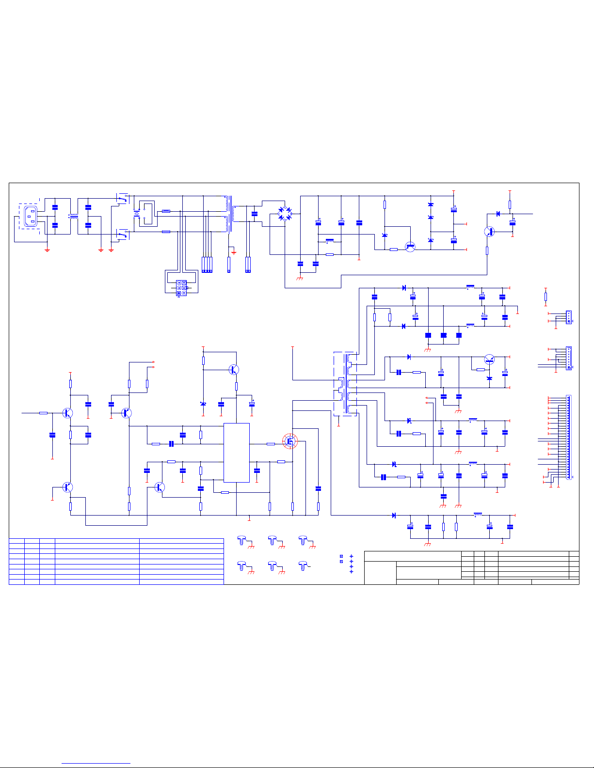
Arcam DiVA DV79 User manual

DiVA Service
Manual
DV79 DVD Player
Issue 1.0
ARCAM
ARCAM
Bringing music & movies to life

Circuit Description
Power Supply L959AY
! CCT diagram
! Component layout diagram
! Parts list
Display Board L961AY
! CCT diagram
! Component layout diagram
! Parts list
Main Board L967AY (for serial numbers below D79V03175)
! CCT diagram
! Component layout diagram
! Parts list
Main Board L974AY (for serial numbers above D79V03174)
! CCT diagram
! Component layout diagram
! Parts list
Transformers
! L924TX
! L925TX
Mechanical Assembly
! Exploded view diagram
! Mechanical and packing part list
DV79
Contents List

Overview
The DiVa DV/79 is a completely new design platform
and only shares it power supply board and display
board with the DV78.
The player is based around acclaimed Zoran Vaddis
Vchipset coupled to high specification Wolfson D to A
converters for all six audio output channels and a
extremely high quality digital video encoder also
featured in this design is a HDMI output digital Video.
Power supply board.
Non-switching
Mains power arrives at IEC inlet socket SKT1 and is
filtered by EMC choke LI and Y caps C3 and C4,
mains switch SW2a/b switches both Negative and Live
phases before the power reaches the mains select
switch at location SW1 the switch allows the primary
windings of the transformer TX1 to be wired in either
Parallel or Series configuration.
The Bridge rectifying Diode package at location D1
forms the basis of the conventional power stage and
supplies a VN35V6 (-35.6v) to the Switch mode
stage, transistor TR1 is biased by 2v7 Zener diode
DZ1 and allows for the series Zener diodes DZ2, DZ3,
DZ3 to supply the VN13V5 and VN19V rails.
We will also see a simple A.C present circuit this is
used for delayed output relay operation and fast relay
closure under interrupted supply conditions thus
preventing power down op-amp offsets from reaching
the Audio output sockets.
Switch mode
The switch mode supply is formed around the
Driver/Control chip IC1 UC3843 (used in regulating
mode). The chip is referenced the –36.5V supply line
and the Digital ground DGND, the supply for the chip
is formed by the 12v Zener at location DZ6 and can be
seen on Pin 7 as VCC. The power supply allows for
the switch-mode to be tied the to Audio sampling
frequency for any given compatible format see Fig 1.
Fig 1 PSU clock control
Fs
Frequency
select
PSUFS1
Pin 11
IC305a
PSUFS0
Pin 12
IC305a
PSUCLK
Output Pin 5
of IC305a
44.1 kHz 0 0 44.1 kHz
48 kHz 0 0 48 kHz
88.2 kHz 0 1 44.1kHz
96 kHz 0 1 48 kHz
176.4 kHz 1 0 44.1 kHz
192 kHz 1 0 48 kHz
Others 1 1 OFF
The PSU sync signal is driven into the power supply via
Resistor R9 if no Sync is present the unit is set to free run at
xxxx due to the RT/RC network attached to Pin 4.
IC1 is running in regulated mode and monitors the voltage
output on the +5V and +3V3 D.C lines, the two voltages are
summed by TR8 and Driven into the VFB and Comp inputs
of IC1, the Voltage is then regulated by changing the time
base of the PWM output at pin 6 (longer the time base the
lower the voltage), the PWM switching frequency is driven
into the switch-mode transformer by the high speed Nmos
device at position M1, R5 is used to sense the Current
across the gate of the Nmosfet and in the event of a short
circuit will safely shut the power supply down. We derive the
12v Mech supply from the output of M1 using the Ultra-fast
Diode at location D8 to rectify the PWM line.
The D.C outputs from the switch mode have extensive
switch mode noise removing filters these are seen as 100n
caps down to ground and Wire wound inductors in series
with the supply rail.
Power supply main board
All the power supply rails are supplied to the main board via
the 32 way FFC conector at location CON1001.
The Digital supplies from the switch mode stage of the
power supply arrive as 3V3D, +5VD and +12VD we also see
the Display board power supplies arrive as –19V, -9 and
–13.5V all of the supplies have a second stage of
implemented on the board to remove all traces of ultra-sonic
noise.
The 3V3D rail is the main 3V3 rail used to power the digital
circuitry; +5VD is used for all 5v Digital/Video supplies the
+12VD is used for Scart switching and to power the HDMI
circuit.
The 1V8 rail is derived from the 3V3 rail and is regulated by
the adjustable regulator at location REG1003.
Diva Dv79 Circuit description.

The Analogue supply stages arrive at the main board
as +15V3 and –15V3 rails these are filtered L1002 and
L1015 before being regulated by the adjustable
regulators at locations REG1000 and REG1002 to
provide +/- 12V rails for the Analogue output stage.
Regulator REG1001 is fed from the +15V3 rail and
forms the Audio DAC supply.
The Display board requires several supply voltages
these are simply passed through the main board,
being filtered on the way to prevent transmission of
noise through to the surrounding electronics. The
display takes the +5V, -19V, -13V5 and -9V the –13V5
and –9V form a floating 4.5V supply biased relative to
the –19V grid voltage.
Display Board
The main component of the Display board is IC1 this is
a Vacuum Florescent Display driver with keyboard san
and a serial data in/out interface.
The Chip receives display drive serial data from the
Vaddis V chip on the main board via Con1 on pins 12,
13 and 14 these will be seen a DIN, STS and CLK this
data is used to drive the VFD a DOUT line interfaces
with the VADDIS V and supplies Keyboard Scan
information. The keyboard scan is a 6 x 4 matrix with
the Key Source appearing at S3, S4, S5, S6 and the
Keyscan data returns appearing a K2, K3 and K4.
Please see: above for power supply information.
The Infra red pick-up at location RXI receives RC5
data and send the data to the Vaddis V on the main
board via transistors TR2 and TR3, LED 2 is used to
mix the rear panel RC5, this is covered in-depth within
the Coms and Video output section of this guide.
Main Board electronics.
Zoran Vaddis V.
The main processor/control chip on the main board is the
Zoran Vaddis V at location IC202, this is the latest
incarnation of the very popular Vaddis range of processors
and allows for a much lower component count when
compared to our earlier players as many of the playback
functions have moved onto the Vaddis V silicon.
Below you will see the major functions of the Vaddis V
o 20 Bit digital video output for external Video
DAC’s and HDMI output stage.
o Decoded Analogue Video output (internal
DAC) used on the DV78 only.
o Digital Audio output 3 data lines 6 channels for
internal L + R DAC’s and L + R + C + LS + RS
for DV79 and DV29 also used for HDMI for the
DV79 and DV29.
o SPDIF output.
o Internal display interface.
o Internal ATAPI interface.
o Internal IR interface.
o Serial in/out for RS232
A more detailed explanation of the Vaddis V and
peripheral components follows.
Vaddis Power
The Vaddis V is powered by two separate supplies the
Vaddis requires a 1.8v supply for the core, this is regulated
from the 3.3v rail by REG1003, the 3.3v rail is used to
supply power to the I/P – O/P ports of the chip.
ATAPI interface
CON203 is an ATAPI interface on a 40 way IDE
connector. This is decoupled from the Drive via an array of
decoupling resistors as required by the ATAPI spec.

Display Board interface
The display board interface is on the 16 way FFC flexi
foil connector at location CON202. Power for the
display also travels on the connector. There are 4 –
wires to interface with the VFD driver chip these are
seen as.
o XFPDIN - Data to the display board
o FPDOUT - Data from the display board
o XFPCLK - Clock
o XFPSEL - Chip select
The above control lines are level shifted to 5v logic
from 3.3v levels by IC200 (74HCT125) these are the
levels required by the VFD drive chip.
The IR output from the Display board arrives as
IRRCV this is an open collector signal, which can be
wire-Ord with the re-panel remote input.
Digital Audio
The Digital audio leaves the chip 3 sets of data lines
labelled as.
o ADAT0 - Left and Right channel data
o ADAT1 - Left and Right surround
o ADAT2 - Centre and Sub
Along with the ADAT line we will also see the ABCLK
and ALRCK as required for IS2 data conversion.
The Vaddis V also supplies a direct SPDIF output for
interfacing with ancillary processing equipment.
Digital Video
The Digital Video output from the Vaddis V consists of
the following signals:
o VIDPO to 19 - 20 Bit wide digital video data
o CLK_27M - 27 Mhz Video clock
o VSYNC - Vertical sync
o HSYNC - Horizontal Sync
The 20 bit wide bus VIDP0 to 19 provides video data
as follows.
Interlaced video mode: VIDP0 to 7 provide
multiplexed 8 bit Y, Cb and Cr data with VIDPO being
the Isb.
Progressive scan video mode: VIDP0 to 9 provide
10 bit multiplexed Cb, Cr data with VIDP0 being the
Isb. VIDP10 to 19 provide 10 bit Y data with VIDP10
being the Isb.
Flash/ SDRAM
IC203 is a 64Mbit (32 bit x 2Meg) SDRAM. It runs at
135MHz
IC205 is a 16Mbit (16 bit x 1Meg) intel type flash IC for
program storage (Player software).
The flash interfaces to the Vaddis V using the SDRAM bus
it may appear that the bus connects to the flash in a
random manner, however this is simply because the
Vaddis bus is multiplexed that way. The Flash will be
accessed at power up and the contents are copied to the
SDRAM the program will then be run from the SDRAM.
Series resistors are employed to isolate the flash bus from
the main SDRAM bus.
EEPROM
IC204 is a 8kBit (1K x 8) Serial EEPROM. This is used for
storage of non-volatile storage of player settings, region
settings and bookmark data.
Clocks
CLK27MV is the 27Mhz clock for video. It is used to
generate the 135Mhz clock for the Vaddis microprocessor
and DSP. The MCLKV is the audio master clock for the
Vaddis.
We run the Vaddis in PLL bypass mode and generate or
own master clock (see main clock section of manual) for
higher accuracy and improved performance across Audio
and Video.
RESET
IC201 is a reset generator chip that monitors the +3.3V rail
and ensures a reset signal PWR_ON_RESET* is
generated on power up, or if the mains power dips below
an operational level.
This signal is used to reset the Vaddis V and Flash micro
only. The Vaddis V line labelled as RESET* resets the
remaining circuitry of the player apart from the HDMI chip,
this has it’s own reset line labelled as HDMI_RESET this is
necessary if we require to reset the HDMI chip only (for
example when the HDMI sink is connected and then
disconnected).
Serial Port
The VADDIS V can interface with the external world via
the RS232 connector at location CON900 and the RS232
Transceiver at location IC900, the serial data lines are
shown as SERIAL RX and SERIAL TX these lines allow
for direct control over the unit via RS232.

Fig 2. GPIO control signals from the Vaddis V
Single Name I/P-
O/P
Function
PSUFSO-1 Output
Control PSU Clock
divider
ENABLE_AV Output
SCART control High
in normal operation
and low in standby
16/9 Output
Scart 16/9
anamorphic control
line
9190INT* Input
Interrupt signal
from SII9190 HDMI
transmitter
GAIN_SCALING Output
High for HDCD gain
scaling
ML_8740_0-2 Output
SPI load signal for
Audio DACs 0,1 and
2 (see note 1)
MC Output
SPI clock signal for
DAC control
MD Output
SPI data signal for
DAC control
FSELE0-1 Output
Frequency select
generator
MUTE* Output
Active low audio
mute signal
DDC_SDA,DDC,SCL I/O
12C bus for DDC
channel on HDMI
interface
PROG_INT* Output
High for Progscan
mode, Low for
interlaced mode.
Controls Sil9130
data mux
HDMI_RESET* Output
Reset signal for
HDMI transmitter
RESET* Output
System reset
Clocks and SPDIF stage.
IC300 is a SM8707E clock generator IC. This IC is
sensitive to noise on it’s power supply, which causes
clock jitter for this reason we have a independent Low
dropout – low noise +3v3 power supply for the chip
based around the regulator at location REG300.
X300 is a 27Mhz crystal that IC300 uses to generate
all the video and audio clocks required by the system
the crystal sits on the XTI and XTO pins of the chip,
the 27Mhz output at Pin 4 (MO2) is used to drive the
Vaddis chip directly bypassing the internal PLL.
The frequency of the audio master is dependent on
the on the current audio sample rate (I.e the sample
rate required by the format CD=44.1Khz and
DVD=48khz etc) and this is set by the system micro
via the FSLO and FSEL1 this selects either the
22.5792Mhz or 24.576Mhz clock from frequency from
IC300 this may then be divided by 2 by the clock
divide chip at location IC306 depending on the status
of FSEL1. Therefore 4 clock frequencies may be
obtained to support all required audio samples rates.
Nand gate IC303 is used to gate FSEL1 with
ENABLE_AV (which is low in standby mode) as such
when in standby mode the audio clock is disabled.
Clock Buffer
IC301 us used to buffer the audio master clock. The circuit
is arranged so that each device that requires the audio
master clock has it’s own driver these are seen as.
o MCLK_DAC0 - Pin 18
o MCLK_DAC1 – Pin 16
o MCLK_DAC2 – Pin 14
o MCLK_VADDIS – Pin 3
o MCLK_HDMI – Pin 9
We also run the Mute Line from the Vaddis V IC301 this
can be seen on Pin 12 and drives transistor TR401, the
transistor pulls the relays RLY400, RLY500, RLY600 to
ground and un-mutes the audio outputs.
IS2 Audio Data
IC302 and IC309 are buffers for the 12S signals these
ensure that the signals travelling to the DAC’s are point to
point. IC302 deals with the ALRCK and ABCLK and
IC309 the ADAT0,1,2 all signal are split into three
separate lines for the three stereo DACS.
PSU Clock Divider
IC304 and IC305 form a clock divide by 1, 2 or 4 to ensure
the PSU clock is always either 44.1kHz or 48Khz (See fig
1 within the power supply description section).
This circuit will also switch the PSUCLK off when
switching between sample rates (the PSU will free run
when the PSUCLK is not present).
SPDIF Output
The SPDIF output consists of IC308 implemented as a
inline buffer and parallel output buffer. Gate A buffers the
signal so that the SPDIF line from the VADDIS sees fewer
loads and form a feed to the Optical output transmitter,
gates B,C and D drive the SPDIF in parallel so that we can
drive a 75ohm load adequately. The resistors at the output
of IC308 are arrange so that the output will be 500mV pk-
pk when the output is terminated with a 75 ohm load at the
same time the output impedance of the circuit is 75ohms
as required by the Sony Philips Digital Interface
specification, C315 provides AC coupling and L301
provides common mode noise rejection for EMC
performance.

Left and Right channel D to A stages
The Wolfson WM8740 stereo DAC requires +5V(A)
and a +3V3 supply along with the Digital Audio data
lines already described in this guide.
The Left channel output only will be described in this
section as all audio output stages are the identical (all
six channels of a DV79) apart from the HDCD gain
switching for L + R only.
IC400B and associated components for a 2
nd
order
Bessel filter with a differential input and a gain of 1 this
follow by a output buffer IC401B, the gain of IC401B is
control by the switching chip at location IC402, in
normal use the Gain of IC401B is set to 1.1 but in
HDCD mode the IC402 switches a second 10k resistor
in parele with R413 and the gain is set to 2.2 allowing
for the higher audio output required by the HDCD
standard.
C436 is a A.C coupling capacitor used to remove the
few mV of offset that the DAC produces, D400
provides protection against from ESD.
The all output relays are under control of the Vaddis
V chip but will also mute the outputs instantly under
mains failure conditions. Switching drive is provided
by TR401 (MUTE_BUF) and TR400 (AC_PRES) the
relays are in mute mode if either the input to TR401 is
Low or if the input to TR400 is high.
Please note: The Scart left/right audio is fed from the
outputs of the left/right audio stages.
Video Encoder
The video encoder at location IC703 is an Analogue
devices ADV7310 video encoder, supporting
interlaced and progressive scan video. It runs on a
2.5V supply provided by REG700 the voltage
reference for the chip of 1.225V is provided by
REF700 and should be seen on Pin 46. C730-731 and
R736 form an external PLL filter.
The Data lines into the encoder arrive as VIDP0 – 19
from the outputs of the VADDIS V chip.
The external current setting resistors for the internal
DACS are seen as R721-R722 and R738-R739 these
set the correct output level for the DACS.
The encoder gives out 6 video signals, for composite,
S-Video (Y and C) and shared YUV/RGB signals. The
setting of the RGB or YUV mode is select with the
Video settings page of the Setup menu.
The six analogue output signals are seen as.
o DAC_A = Composite
o DAC_B = SVID Y
o DAC_C = SVID C
o DAC_D = Y or Green
o DAC_E = U or Blue
o DAC_F = V or Red
Please note: When the player is in Progressive scan
mode the composite and S-Video signals will be
switched off.
The Video outputs from IC703 are filtered by six identical
filters. For instance if we look at the Composite stage we
will see a very slow roll off filter comprising of C719,
C721 with L701 and L703 the –3dB point of the filter
stage is around 40Mhz, resistors R700 and R702 form a
load for the current output DAC and as such set the
relative output level.
The outputs are driven by the Video op-amp at location
IC700A this has a gain of 2.15 and is terminated by a
75ohm resistor, D701 forms protection against ESD.
These signals now travel to the COMMS and Video
extension card on Con 901. See description on
page 7.
SCART Output
RGB and Composite video signals as well as Left and
Right audio signals are all present on the SCART output
socket. As the RGB and YUV signals share the same
output port at the Vaddis V the player must be set to
RGB SCART operation to have a RGB output on the
SCART. Please note: When in RGB SCART mode the
RGB does not contain a Sync signal and the sync must
be taken from the Composite out (4 wire RGB).
Also present at the Scart are a number of control flags
for the monitor these include 2 GPIO control lines direct
from the Vaddis.
o ENABLE_AV
o 16/9
These are seen at the SCART output pins as.
o O/6/12
o RGB STAT
The 0/6/12 line (SCART pin 8) is used to inform the
monitor of the screen format being sent by the player as
set in the video set-up section of the software.
o Standby = 0V
o 16:9 aspect ratio = 6V
o 4:3 aspect ration = 12V
The RGB status line (SCART pin 16) will be seen as 0v
= no RGB and >1v is RGB present.

HDMI output stage
Please note: Due to the plug and play nature of the
HDMI/DVI interface, if presented with a reported no
HDMI problem it is worth checking all set-up
parameters of both the DVD player and the
Plasma/Projector in use before performing component
level diagnostics on this product.
HDMI is a system that transmits uncompressed digital
video and digital audio over a high speed encrypted
interface.
IC1102 is an SII9190 HDMI transmitter IC in essence
the chip takes the Digital Video and Audio information
and sends the Data out in HDMI format.
REG1100 is used to generate a clean regulated 3V3
power supply to Pins 18 and 33 of the HDMI chip.
IC1100 –IC1101 are 3 state octal/line drivers these
form a multiplex that switches between the 2 groups of
signals for the video data input stage of the SII9190
the multiplexer is control by the Signal from the Vaddis
V labelled as PROG/INT this will sit at logic 1 for
Progressive scan and logic 0 for interlaced.
In interlaced mode the 8 bit Y/Cb/Cr video data on
VIDP7-0 are passed to input port pins D15 – D8 of the
SII9190.
In Progressive scan mode all 20 bits of the Video
data bus are used and get mapped as follow.
VIDP 19 -12 provide 8 msbits of Y data to pins D15-8
VIDP 11 -10 provide 2Isbits of Y data to pins D2-3
VIDP 9 - 2 provide 8 msbits of Cb/Cr data to pins D23 – 16
VIDP 1 – 0 provide 2 Isbits of Cb/Cr data to pins D7 - 6
Along with the VIDP video data lines we must also see
VSYNC – Vertical sync data
HSYNC – Horizontal sync
CLK27M_VID – 27Mhz video clock.
SPDIF – Digital audio data
MCLK_HDMI – Used to strobe HDMI dig audio
At the output of the HDMI chip we will see the
following signals at SKT100.
TMDS (Transistion Minimised Differential Signalling)
this consists of a clock signal (TXC+/TXC-) and 3 data
signals (TX0+/TX0-, TX1+/TX1- and TX2+/TX2-).
All signals are differential and use current switching
techniques therefore no signals will be observed
unledd the output is correctly terminated. In this
application the clock signal will always be 27MHz and
the data signals will be clock X10 so 270Mbit/s.
DDC Channel this is a 12C interface on DDC_SCL and
DDC_SDA. These signals connect to the VADDIS V
which is the I2C bus master, The DDC channel is used
to read back information from the HDMI sync regarding
it’s Video and Audio capabilities and is also used for
HDCP encryption authentication.
+5V Power, the HDMI interface requires a 5V supply
capable of delivering around 50mA, the supply is
provided by REG 1101 which delivers the required
current and will shut down in the event of a short circuit.
Hotplug. The HDMI `Hot plug’ signal HDPIN is a +5V to
signal the presence of equipment being connected, this
converted to 3v3 logic 1 as IC1100 is not +5V tolerant.
CEC. The CEC (Consumer Electronics Control) signal is
a 1-wire bidirectional control signal. It connects to the
Vaddis via an ESD protection circuit D1102 at the
moment this line is not used at present and is a optional
part of the HDMI specification.
Comms and Final video output stage
The signals from the main board travel up to the Comms
board on connector CON902.
The Video signals simply travel via an A-C coupling net
before exiting the player via the RCA-phono sockets at
locations SKT902 and SKT903.
The RS232 interface is on 9 way “D” type CON900, with
IC900 providing the level translation and static protection
between the RS232 levels and the 3.3V CMOS levels
required by the VADDIS V, CON900 also supplies a +5V
Status level when ever the unit is not in standby this
generated from a buffered version of the AV_ENABLE
signal as used within the SCART output stage (0V in
standby).
We have two remote input bus’s on this board, the first
can be seen to arrive at SK901 on a 3.5mm mono jack
signal received should be a 36Khz modulated RC5
signal, the RC5 data then travels to the front panel and
is fed to IR led that is sited just behind the front panel IR
Sensor, we use the sensor to demodulate the and opto-
isolate the signal due to the fact that the signal is floating
up from ground.
The 3.5mm socket at location SKT900 is used to receive
un-modulated RC5 signals these take the form of a
5V/0V RC5 signal, with 5V representing a mark
(equivalent to a burst of 36Khz carrier on infrared) and
the 0V representing a space (equivalent to no-infra-red
carrier), this input is effectively wire-Ord with the front
panel IR receiver on IRRCV.

ISSUE
DRAWING NO.
DRAWING TITLE
DATE
Filename:
ECONo. DESCRIPTION OF CHANGE
L959_1.1.sch
DV78 SERIES PSU
Contact Engineer:
L959CT
22-Apr-2004
INITIALS
Printed:
1 1Sheet of
Notes:
Contact Tel: (01223)203200Kevin Lamb
A & R Cambridge Ltd.
Pembroke Avenue
Cambridge CB5 9PB
Waterbeach
DGND
DGND
DGND
DGND
DGND
VN35V6
VN35V6 VN35V6VN35V6
DGND
115V
115V
6
4
2
1
5
3
7
TX1
Small Toroidal Mains
L924TX
D1
2KBP02
VN35V6
DGND
1
2
3
4
5
6
CON1
MOLEX
44472
L
N
E
SKT1
BULGIN
PX0580
C2
C1 C3
3N3
250V
CER
C4
3N3
250V
CER
1
3
4
2
L1
250U
SW2A
SDDFC30400
SW2B
SDDFC30400
1A
1
1B
2A
2
2B
115V 230V
SW1
18-000-0019
FHLDR2
20mm HLDR
FHLDR1
20mm HLDR
FS1 T315mA
S504
FS2
T315mA
S504
VN19V
EMC Shield
SH1
1
2
3
4
CON5
Amp
HD Pwr Con
VP5V
VP12V
DGND
1
2
3
4
5
6
7
8
9
10
11
12
13
14
15
16
17
18
19
20
21
22
23
24
25
26
27
28
29
30
31
32
CON7
MOLEX
52045
VN19V
VN13V5_F1
VN9V_F2
DGNDAGND
VP12V
VP15V5
VP5V
VP3V3
VP3V3
VN15V5
VP5V
VP3V3
VP3V3
VP3V3
VP3V3
VP5V
SPARE3
SPARE4
AC_PRES*
PSU_CLK
DGND
VP3V3
VP5V
SPARE1
SPARE2
C46
470UF
25V
YK
C39
220UF
16V
YXF
C54
1000UF
16V
YXF
C55
1000UF
16V
YXF
C45
470UF
25V
YK
C44
470UF
25V
YK
D4
UF4003
DO-41
C34
1N0 100V
CER
C36
1N0
100V
CER C25
100N
100V
MKS2
C20
100N
100V
MKS2
C22
100N
100V
MKS2
C21
100N
100V
MKS2
C23
100N
100V
MKS2
C26
100N
100V
MKS2
C24
100N
100V
MKS2
C19
100N
100V
MKS2
C18
100N
100V
MKS2
R31
10R
0W25
MF
R18
10R 0W25
MF
R22
470R 0W25
MF DZ5
BZX79C
5V1
DO-35
TR6
BD179
TO-126
R24
33R 0W25
MF
R5
4K7 0W25
MF
C40
220UF
16V
YXF
C17
100N
100V
MKS2
DZ6
BZX79C
12V
DO-35
R11
9K1
0W25
MF
R7
6K8
0W25
MF
R4
4K7 0W25
MF
R26
68R
0W25
MF
R27
2K7
0W25
MF
R25
100R
0W25
MF
R28
22R
0W25
MF
R15
10K
0W25
MF
C50
22N 100V
MKS2
C16
100N
100V
MKS2
C56
4N7
100V
CER
TR8
BC556B
TO-92
M1
IRF640N
TO-220
C6
100N
100V
MKS2
C7
100N
100V
MKS2
COMP
1
VFB
2
ISEN 3
RT/CT
4
GND
5
OUT 6
VCC 7
VREF
8
IC1
UC3843AN
DIP-8
TR7
BC556B
TO-92
DGND
TR3
BC546B
TO-92
R13
10K
0W25
MF
VP5V
PSU_CLK
C35
1N0 100V
CER
R19
10R 0W25
MF
C33
1N0 100V
CER
R23
33R 0W25
MF
AGND
C41
470UF
25V
YK
C9
100N
100V
MKS2
C10
100N
100V
MKS2
C12
100N
100V
MKS2
R20
470R
0W25
MF
D2
UF4003
DO-41
C42
470UF
25V
YK
C13
100N
100V
MKS2
D3
UF4003
DO-41 C11
100N
100V
MKS2
VP15V5
VN15V5
VN13V5_F1
VN9V_F2
VP5V
VP3V3
VP12V
VN35V6
R3
4K7
0W25
MF
TR2
BC546B
TO-92
R6
6K8
0W25
MF
C31
22UF
63V
YK
VP5V
DGND
AC_PRES*
R9
1K0 0W25
MF
TR4
BC546B
TO-92
C47
22P
100V
N150
DGND
R8
1K0
0W25
MF
C14
100N
100V
MKS2
R10
1K0 0W25
MF
C15
100N
100V
MKS2
VN35V6
5V_NFB
3V3_NFB
3V3_NFB
5V_NFB
C51
22N
100V
MKS2
L6
6U8 2.1A 8RHT2
L7
6U8 2.1A 8RHT2
L5
33U 1.17A 8RHT2
L3
33U 1.17A 8RHT2
L4
33U 1.17A 8RHT2
VN35V6
VN35V6
VN13V5_F1
C29
22UF
63V
YK
MAINS SUPPLY
FOR EXT. AUDIO
SUPPLY TX
C49
22N
100V
MKS2
R14
R29
82K 0W25
MF
NF
NFB (To Controller E/A)
(NFB From PSU Outputs)
GREY 4
DK GREY 3
LT GREY 2
BLUE 1
CON2
WAGO
256
GREY 2
GREY 1
CON4
WAGO
256
GREEN 1
CON3
WAGO
256
GREY
WHITE
BLACK
BLUE
R16
47K
0W25
MF
C53
1000UF
16V
YXF
C8
100N
100V
MKS2
QTY DESCRIPTIONPART No. NOTESITEM
ITEM1 1 Clip For SW Profile HeatsinkF006
ITEM3 2 Fuseholder Cover For 20mm FuseholderF022
ITEM2 1 Sil Pad For TO-220 HS InsulatorF082
ITEM4 1 Blank PCB DV78 PSUL959PB
C37
100UF
50V
YXF
C38
100UF
50V
YXF
C57
470UF
25V
YXF
C30
22UF
63V
YK
C43
470UF
25V
YK
NF
NF
1
2
3
4
5
6
7
8
CON6
AMP
CT
NF
R32
C5
AGND
DGND
LK2
ITEM5 1 Earth Lead Assy 75MM8M101 SAFETY EARTH WIRE FROM IEC INLET SK1 TO METAL CHASSIS
L2
LK1
0R0 0W25 MF
D5
1N4148
DO-35
1
FIX2
Dia 3.5mm
1
FIX4
Dia 3.5mm
1
FIX5
Dia 3.5mm
7
2
3
16T
16T
22T
14T
10T
8
1 11
10
9
12
4
41T
41T
5
6
SCR
TX2
Ferrite Switch Mode
L925TX
DGND
FD1
FD2
TOOL1
TOOL2
TOOL3
TOOL4
C27
1000UF
63V
YK
C28
1000UF
63V
YK
C48
1N0
100V
CER
TR5
BD179
TO-126
R12
10K
0W25
MF
D6
31DQ10 DO-201AD
D7
31DQ06 DO-201AD
D8
UF5406
DO-201AD
R21
470R
0W25
MF
C32
470pF
1kV
DE
DZ4
BZX79C
5V6
DO-35
1
FIX1
Dia 3.5mm
1
FIX3
Dia 3.5mm
1
FIX6
Dia 3.5mm
NF
NF
R17
10R
0W25
MF
TR1
BC547B
TO-92
DZ1
BZX79C
2V7
DO-35
R1
22K
0W25
MF
R2
220R
0W25
MF
HS1B
SW38-2
10.2C/W
NOTE TRANSFORMER TX1 IS MOUNTED ON
THE CHASSIS AND CONNECTED TO THE PSU
PCB BY CON2,3,4. TX1 IS SHOWN ABOVE FOR
CIRCUIT OPERATION
NF
R33
1K0
0W25
MF
USED TO SECURE TRANSFORMER CABLES TO PCB NEAR CON1
NF
ITEM7 2 Rivet CopperHP007S RIVETS TO SECURE IEC INLET TO PCB
DZ2
BZX79C
10V
DO-35
DZ3
BZX79C
3V3
DO-35
NF
C52
330P
100V
N750
R30
0R22
3W
SPRX
1.0
Production release02/07/03KAL03_E195
1.1
Make CON1 fitted (used in DV29)22/04/04PG04_E046
ITEM6 1 Cable Tie 100MM X 2.5MMF044


DV79 DVD player PSU board L959AY issue 1.1.1
Designator Part Description
C1 2J410 Capacitor SM 0805 X7R Ceramic 10% 50V 100N
C2 2J410 Capacitor SM 0805 X7R Ceramic 10% 50V 100N
C3 2J410 Capacitor SM 0805 X7R Ceramic 10% 50V 100N
C4 2J410 Capacitor SM 0805 X7R Ceramic 10% 50V 100N
C5 2MA610 Capacitor Surface Mount Electrolytic 10UF 50V 6.3 X 4.5MM
C6 2MA610 Capacitor Surface Mount Electrolytic 10UF 50V 6.3 X 4.5MM
C7 2MA610 Capacitor Surface Mount Electrolytic 10UF 50V 6.3 X 4.5MM
C8 2L210 Capacitor SM 0805 NPO Ceramic 5% 100V 1N0
C9 2L210 Capacitor SM 0805 NPO Ceramic 5% 100V 1N0
C10 2L210 Capacitor SM 0805 NPO Ceramic 5% 100V 1N0
C11 2L210 Capacitor SM 0805 NPO Ceramic 5% 100V 1N0
CON1 8K8616 Con 1.0MM Horiz FFC 16WAY 52807 Series
D1 3AS16W Diode Surface Mount Small Signal BAS16W SOT-23 Package
D2 3AS16W Diode Surface Mount Small Signal BAS16W SOT-23 Package
D3 3AS16W Diode Surface Mount Small Signal BAS16W SOT-23 Package
D4 3AS16W Diode Surface Mount Small Signal BAS16W SOT-23 Package
DISP1 B1014 Display DV88
IC1 5H6312 IC VFD Driver PT6312LQ SM LQFP-44 package
LED1 3D007 LED 3.1mm Green SLR-37MG3T
LED2 3D010 LED SM Red SML-010LT
LED3 3D007 LED 3.1mm Green SLR-37MG3T
LED5 3D006 LED 3mm Red/Green Tri-Colour L-93WEGW
R1 1M133 Resistor 0805 Surface Mount 0.125W 1% 330R
R2 1M133 Resistor 0805 Surface Mount 0.125W 1% 330R
R3 1M133 Resistor 0805 Surface Mount 0.125W 1% 330R
R4 1M122 Resistor 0805 Surface Mount 0.125W 1% 220R
R5 1M118 Resistor 0805 Surface Mount 0.125W 1% 180R
R6 1M139 Resistor 0805 Surface Mount 0.125W 1% 390R
R8 1M310 Resistor 0805 Surface Mount 0.125W 1% 10K
R9 1M310 Resistor 0805 Surface Mount 0.125W 1% 10K
R10 1M247 Resistor 0805 Surface Mount 0.125W 1% 4K7
R11 1M356 Resistor 0805 Surface Mount 0.125W 1% 56K
R13 1M310 Resistor 0805 Surface Mount 0.125W 1% 10K
R14 1M310 Resistor 0805 Surface Mount 0.125W 1% 10K
R15 1M310 Resistor 0805 Surface Mount 0.125W 1% 10K
RX1 B2109 IR Receiver Module Kodenshi KSM-902TM1N
SW1 A1511 Switch Tact Low Profile No Gnd Pin
SW2 A1511 Switch Tact Low Profile No Gnd Pin
SW3 A1511 Switch Tact Low Profile No Gnd Pin
SW4 A1511 Switch Tact Low Profile No Gnd Pin
SW5 A1511 Switch Tact Low Profile No Gnd Pin
SW6 A1511 Switch Tact Low Profile No Gnd Pin
SW7 A1511 Switch Tact Low Profile No Gnd Pin
SW8 A1511 Switch Tact Low Profile No Gnd Pin
SW9 A1511 Switch Tact Low Profile No Gnd Pin
TR2 4D10KN Digital Transistor MMUN2211LT1 SOT23 Package
TR3 4A849B Transistor BC849B SOT23 Package
TR4 4A849B Transistor BC849B SOT23 Package
TR5 4D10KP Digital Transistor MMUN2111LT1 SOT23 Package

ISSUE
DRAWING NO.
DRAWING TITLE
DATE
Filename:
ECONo. DESCRIPTION OF CHANGE
L961_1.3.Sch
DV78/DV79 DISPLAY BOARD
Contact Engineer:
L961
17-Sep-2004
INITIALS
Printed:
1 1Sheet of
Notes:
Contact Tel: (01223)203270PeterGaggs
A & R Cambridge Ltd.
Pembroke Avenue
Cambridge CB5 9QR
Waterbeach
A2
F1
1
F1
2
G1
5
G2
6
G3
7
G4
8
G5
9
G6
10
G7
11
S1
25
S2
26
S3
27
S4
28
S5
29
S6
30
S7
31
S8
32
S9
33
S10
34
S11
35
S12
36
S13
37
S14
38
S15
39
F2
42
F2
43
DISP1
SAMSUNG
SVV-07MS09
SW1
1
SW2
2
SW3
3
SW4
4
DOUT
5
DIN
6
GND
7
CLK
8
STB
9
K1
10
K2
11
K3
12
K4
13
VDD
14
SG1/KS1
15
SG2/KS2
16
SG3/KS3
17
SG4/KS4
18
SG5/KS5
19
SG6/KS6
20
SG7
21
SG8
22
SG9 23
SG10 24
SG11 25
SG12/GR11 26
VEE 27
SG13/GR10 28
SG14/GR9 29
SG15/GR8 30
SG16/GR7 31
GR6 32
GR5 33
GR4 34
GR3 35
GR2 36
GR1 37
VDD 38
LED4 39
LED3 40
LED2 41
LED1 42
GND 43
OSC 44
IC1
PT6312LQ
LQFP-44
S1
S2
S3
S4
S5
S6
S7
S8
S9
S10
S11
S12
S13
S14
S15
G1
G2
G3
G4
G5
G6
G7
S1
S2
S3
S4
S5
S6
S7
S8
S9
S10
S11
S12
S13
S14
S15
G1
G2
G3
G4
G5
G6
G7
-9V_F2-13V5_F1
+5VD
DGND
+5VD
DGND
-19V
DGND
VFD
REDGRN
LED5
3mm
BICOL
LED 3mm
LED1
3mm
GRN
LED 3mm
+5VD DVD-A
LED3
3mm
GRN
LED 3mm
+5VD NAV
POWER
DGND
+5VD
+5VD
NAV_LED*
ON/STBY*_LED
DVDA_LED*
DGND
+5VD DGND
DGND
K4
K3
K2
K[2..4]
1
2
SW6
S3
1
2
SW7
1
2
SW8
1
2
SW9
K4
PLAY
K3
K2
S4
S5
S6
STOP
1
2
SW3
>|
1
2
SW1
MODE
LOAD
1
2
SW4
PAUSE
>>
|<
1
2
SW5
1
2
SW2
<<
IR REMOTE SENSOR
+5VD
DGND
NF
+5VD
1
2
3
4
5
6
7
8
9
10
11
12
13
14
15
16
CON1
MOLEX
52807
DGND
DOUT
DIN
CLK
STB
P2
P3
P4
P5
IRRCV
P7
P1
+5VD
P8
DGND
P9
DGND
-19V
-13V5_F1
P10
-9V_F2
P11
ITEM1 BLANK PCB DV78 DISPLAY BOARD1 L961PB
Note that G1..7 are deliberately
reversed here, to be the same as
previous design (software takes it into
account)
ITEM2 1
ITEM3 1
LED2
SM
RED
SML-010
P6 REM_P
LED2 is underneath infra red receiver.
The LED is lit by the remote bus signal,
allowing the infra red receiver to
demodulate the remote bus signal.
DGND
DGND DGND DGNDDGND
F231
F231
VFD CORNER LOCATOR
VFD CORNER LOCATOR
CHS
R13
10K
0W125
0805
R14
10K
0W125
0805
R15
10K
0W125
0805
D1
BAS16
SOT-323
D2
BAS16
SOT-323
D3
BAS16
SOT-323
D4
BAS16
SOT-323
R3
330R
0W125
0805
R1
330R
0W125
0805
R4
220R
0W125
0805
TR4
BC849B
SOT-23
TR5
MMUN2111LT1
SOT-23
C2
100N
50V
0805
C3
100N
50V
0805
C4
100N
50V
0805
R10
4K7
0W125
0805
R11
56K
0W125
0805
R2
330R
0W125
0805
R8
10K
0W125
0805
R9
10K
0W125
0805
C1
100N
50V
0805
TR2
MMUN2211LT1
SOT-23
TR3
BC849B
SOT-23
C8
1N0
100V
0805
C9
1N0
100V
0805
C10
1N0
100V
0805
C11
1N0
100V
0805
C5
10UF
50V
SM
C6
10UF
50V
SM
C7
10UF
50V
SM
70mm of 10mm wide double sided tape under VFD
REM_N
R5
180R
0W125
0805
NF
R6
390R
0W125
0805
+5VD
Pins 1-4 (SW1-4) are set
to read 0001, to be read
by display self test in
software
FD1 FD2
TOOL1 TOOL2 TOOL3 TOOL4
P18
P16
P20
P13
P17
P12
P14 P15
P19
NOTE TO ENGINEERS:
When creating BOM, import CSV into database then manually change quantity to 0.07 for ITEM4 (F238
tape)
This is the only way to ensure it appears as 0.07m on the BOM report
PG 04-07-03 INITIAL SCH 1.003_E202
PG 02-09-03 CHANGE FOAM TAPE FROM F163 TO F238 (DOUBLE SIDED) 1.103_E260
ITEM4 1 Foam D/S ADH BK 3MM Thk 10MM Wide RA106 10M ReelF238
PG 12-01-04 ADD DVD-A LED FOR DV79 1.204_E007
PG 17-09-04 CHANGE RX1 TO KSM-902TM1N FOR BETTER PERFORMANCE 1.304_E140
+5V
O/P
GND
RX1
KSM-902TM1N


DV79 DVD player Display board L961AY issue 1.3.0
Designator Part Description
C1 2J410 Capacitor SM 0805 X7R Ceramic 10% 50V 100N
C2 2J410 Capacitor SM 0805 X7R Ceramic 10% 50V 100N
C3 2J410 Capacitor SM 0805 X7R Ceramic 10% 50V 100N
C4 2J410 Capacitor SM 0805 X7R Ceramic 10% 50V 100N
C5 2MA610 Capacitor Surface Mount Electrolytic 10UF 50V 6.3 X 4.5MM
C6 2MA610 Capacitor Surface Mount Electrolytic 10UF 50V 6.3 X 4.5MM
C7 2MA610 Capacitor Surface Mount Electrolytic 10UF 50V 6.3 X 4.5MM
C8 2L210 Capacitor SM 0805 NPO Ceramic 5% 100V 1N0
C9 2L210 Capacitor SM 0805 NPO Ceramic 5% 100V 1N0
C10 2L210 Capacitor SM 0805 NPO Ceramic 5% 100V 1N0
C11 2L210 Capacitor SM 0805 NPO Ceramic 5% 100V 1N0
CON1 8K8616 Con 1.0MM Horiz FFC 16WAY 52807 Series
D1 3AS16W Diode Surface Mount Small Signal BAS16W SOT-23 Package
D2 3AS16W Diode Surface Mount Small Signal BAS16W SOT-23 Package
D3 3AS16W Diode Surface Mount Small Signal BAS16W SOT-23 Package
D4 3AS16W Diode Surface Mount Small Signal BAS16W SOT-23 Package
DISP1 B1014 Display DV88
IC1 5H6312 IC VFD Driver PT6312LQ SM LQFP-44 package
LED1 3D007 LED 3.1mm Green SLR-37MG3T
LED2 3D010 LED SM Red SML-010LT
LED3 3D007 LED 3.1mm Green SLR-37MG3T
LED5 3D006 LED 3mm Red/Green Tri-Colour L-93WEGW
R1 1M133 Resistor 0805 Surface Mount 0.125W 1% 330R
R2 1M133 Resistor 0805 Surface Mount 0.125W 1% 330R
R3 1M133 Resistor 0805 Surface Mount 0.125W 1% 330R
R4 1M122 Resistor 0805 Surface Mount 0.125W 1% 220R
R5 1M118 Resistor 0805 Surface Mount 0.125W 1% 180R
R6 1M139 Resistor 0805 Surface Mount 0.125W 1% 390R
R8 1M310 Resistor 0805 Surface Mount 0.125W 1% 10K
R9 1M310 Resistor 0805 Surface Mount 0.125W 1% 10K
R10 1M247 Resistor 0805 Surface Mount 0.125W 1% 4K7
R11 1M356 Resistor 0805 Surface Mount 0.125W 1% 56K
R13 1M310 Resistor 0805 Surface Mount 0.125W 1% 10K
R14 1M310 Resistor 0805 Surface Mount 0.125W 1% 10K
R15 1M310 Resistor 0805 Surface Mount 0.125W 1% 10K
RX1 B2109 IR Receiver Module Kodenshi KSM-902TM1N
SW1 A1511 Switch Tact Low Profile No Gnd Pin
SW2 A1511 Switch Tact Low Profile No Gnd Pin
SW3 A1511 Switch Tact Low Profile No Gnd Pin
SW4 A1511 Switch Tact Low Profile No Gnd Pin
SW5 A1511 Switch Tact Low Profile No Gnd Pin
SW6 A1511 Switch Tact Low Profile No Gnd Pin
SW7 A1511 Switch Tact Low Profile No Gnd Pin
SW8 A1511 Switch Tact Low Profile No Gnd Pin
SW9 A1511 Switch Tact Low Profile No Gnd Pin
TR2 4D10KN Digital Transistor MMUN2211LT1 SOT23 Package
TR3 4A849B Transistor BC849B SOT23 Package
TR4 4A849B Transistor BC849B SOT23 Package
TR5 4D10KP Digital Transistor MMUN2111LT1 SOT23 Package

ISSUE
DRAWING NO.
DRAWING TITLE
DATE
Filename:
ECONo. DESCRIPTION OF CHANGE
L967C1.Prj
DV79 MAIN BOARD TOP LEVEL
Contact Engineer:
L967C1
19-Feb-2004
INITIALS
Printed:
1 11Sheet of
Notes:
Contact Tel: (01223)203270PeterGaggs
A & R Cambridge Ltd.
Pembroke Avenue
Cambridge CB5 9QR
Waterbeach
A2
MUTE*
ML_8740_0
MC
MD
ML_8740_2
FSEL0
ML_8740_1
ENABLE_AV
16/9
GAIN_SCALING
SERIAL_RX
SERIAL_TX
IRRCV
SPDIF
ADAT1
ADAT2
ADAT0
ABCLK
ALRCLK
CLK27M_VADDIS
MCLK_VADDIS
RESET*
PSUFS0
PSUFS1
CLK_27M_VID
VSYNC*
HSYNC*
VIDP[0..19]
REM_BUS_P
REM_BUS_N
9190INT*
FSEL1
PROG/INT*
DDC_SDA
DDC_SCL
SDA
SCL
CEC
HDMI_RESET*
L967C2
L967C2.sch
FSEL0
CLK27M_VADDIS
MCLK_VADDIS
MCLK_DAC0
MCLK_DAC1
MCLK_DAC2
ABCLK
ALRCLK
ABCLK_DAC0
ABCLK_DAC1
ABCLK_DAC2
ALRCLK_DAC0
ALRCLK_DAC1
ALRCLK_DAC2
PSUCLK
PSUFS0
PSUFS1
MUTE*
MUTE_BUF*
FSEL1
MCLK_HDMI
ABCLK_HDMI
ADAT0
ADAT1
ADAT_DAC0
ADAT_DAC1
ADAT2
ADAT_DAC2
SPDIF
ENABLE_AV
L967C3
L967C3.Sch
ALRCLK_DAC0
ADAT_DAC0
ABCLK_DAC0
MCLK_DAC0
MD
MC
ML_8740_0
RESET*
GAIN_SCALING
MUTE_BUF*
AC_PRES* SCART_LEFT
SCART_RIGHT
L967C4
L967C4.Sch
ALRCLK_DAC1
ADAT_DAC1
ABCLK_DAC1
MCLK_DAC1
MD
MC
ML_8740_1
RESET*
CENTRE_OUT
SUB_OUT
L967C5
L967C5.Sch
ALRCLK_DAC2
ADAT_DAC2
ABCLK_DAC2
MCLK_DAC2
MD
MC
ML_8740_2
RESET*
CENTRE_OUT
SUB_OUT
L967C6
L967C6.Sch
SCART_LEFT
SCART_RIGHT
SCART_BLUE
SCART_GREEN
SCART_RED
SCART_COMPOSITE
ENABLE_AV
16/9
L967C8
L967C8.Sch
PSUCLK
AC_PRES*
L967C10
L967C10.Sch
HDMI_RESET*
9190_INT*
SCL
SDA
VIDP[0..19]
VSYNC*
HSYNC*
CLK27M_VID
MCLK_HDMI
SPDIF
PROG/INT*
DDC_SCL
DDC_SDA
ADAT0
ADAT1
ADAT2
ALRCLK
ABCLK_HDMI
CEC
L967C11
L967C11.Sch
FSEL0
FSEL1
PSUFS0
PSUFS1
ADAT0
ADAT1
ADAT2
ABCLK
ALRCLK
SPDIF
MUTE*
CLK27M_VADDIS
MCLK_VADDIS
GAIN_SCALING
RESET*
MD
MC
ML_8740_0
ML_8740_1
ML_8740_2
PSUCLK
AC_PRES*
ADAT_DAC0
ABCLK_DAC0
ALRCLK_DAC0
MCLK_DAC0
MUTE_BUF*
MD
MC
ADAT_DAC1
ABCLK_DAC1
ALRCLK_DAC1
MCLK_DAC1
ADAT_DAC2
ABCLK_DAC2
ALRCLK_DAC2
MCLK_DAC2
ADAT0
ADAT1
ADAT2
ABCLK_HDMI
ALRCLK
MCLK_HDMI
RESET*
9190INT*
PROG/INT*
DDC_SDA
DDC_SCL
SDA
SCL
VIDP[0..19]
HSYNC*
VSYNC*
CLK_27M_VID
16/9
ENABLE_AV
SCART_LEFT
SCART_RIGHT
SCART_COMPOSITE
SCART_RED
SCART_GREEN
SCART_BLUE
COMPOSITE
Y
U
V
SVID_Y
SVID_C
MD
MC
RESET*
RESET*
IRRCV
SERIAL_TX
SERIAL_RX
REM_BUS_P
REM_BUS_N
VADDIS V
SHEET 2
CLOCKS
SHEET 3
DAC L&R
SHEET 4
DAC LS&RS
SHEET 5
DAC C & SUB
SHEET 6
HDMI
SHEET 11
VIDEO ENCODER
SHEET 7
SCART
SHEET 8
COMMS, VIDEO OUT
SHEET 9
POWER
SHEET 10
CEC
PG 1.0
ENABLE_AV
V
U
Y
COMPOSITE
SVID_Y
SVID_C
REM_BUS_P
REM_BUS_N
IRRCV
ENABLE_AV
SERIAL_RX
SERIAL_TX
L967C9
L967C9.Sch
VIDP[0..19]
HSYNC*
VSYNC*
CLK27M_VID
SDA
SCL
RESET*
COMPOSITE
SCART_COMPOSITE
SVID_Y
SVID_C
Y
SCART_GREEN
U
SCART_BLUE
V
SCART_RED
L967C7
L967C7.Sch
ITEM100 1 Blank PCB DV79 Main BoardL967PB
03_E020 19-02-04 Production release
HDMI_RESET*

ISSUE
DRAWINGNO.
DRAWINGTITLE
DATE
Filename:
ECONo. DESCRIPTIONOF CHANGE
L967C2.sch
DV79 MAIN VADDIS V
Contact Engineer: L967C2
19-Feb-2004
INITIALS
Printed: 2 11Sheet of
Notes:
Contact Tel: (01223) 203270PeterGaggs
A & R Cambridge Ltd.
PembrokeAvenue
Cambridge CB5 9QR
Waterbeach
A1
ISSUE
DRAWINGTITLE
DATE
Filename:
ECONo. DESCRIPTIONOF CHANGE
L967C2.sch
DV79 MAIN VADDIS V
Contact Engineer: 19-Feb-2004
INITIALS
Printed: 2 11Sheet of
Notes:
Contact Tel: (01223) 203270PeterGaggs
A & R Cambridge Ltd.
PembrokeAvenue
Waterbeach
RAMADD0
RAMADD1
RAMADD2
RAMADD3
RAMADD4
RAMADD5
RAMADD6
RAMADD7
RAMADD8
RAMADD9
RAMADD10
RAMBA0
RAMBA1
RAMADD0
RAMADD1
RAMADD2
RAMADD3
RAMADD4
RAMADD5
RAMADD6
RAMADD7
RAMADD8
RAMADD9
RAMADD10
RAMBA1
RAMBA0
DGND
+3V3D
+1V8D
DGND
+3V3D
VDDP_A
VDD_PLL
+3V3D
DGND
RAMDAT0
RAMDAT1
RAMDAT2
RAMDAT3
RAMDAT4
RAMDAT5
RAMDAT6
RAMDAT7
RAMDAT8
RAMDAT9
RAMDAT10
RAMDAT11
RAMDAT12
RAMDAT13
RAMDAT14
RAMDAT15
RAMDAT16
RAMDAT17
RAMDAT18
RAMDAT19
RAMDAT20
RAMDAT21
RAMDAT22
RAMDAT23
RAMDAT24
RAMDAT25
RAMDAT26
RAMDAT27
RAMDAT28
RAMDAT29
RAMDAT30
RAMDAT31
RAMDAT31
RAMDAT0
RAMDAT1
RAMDAT2
RAMDAT3
RAMDAT4
RAMDAT5
RAMDAT6
RAMDAT7
RAMDAT8
RAMDAT9
RAMDAT10
RAMDAT11
RAMDAT12
RAMDAT13
RAMDAT14
RAMDAT15
RAMDAT16
RAMDAT17
RAMDAT18
RAMDAT19
RAMDAT20
RAMDAT21
RAMDAT22
RAMDAT23
RAMDAT24
RAMDAT25
RAMDAT26
RAMDAT27
RAMDAT28
RAMDAT29
RAMDAT30
RAMDQM
RAMCS*
RAMRAS*
RAMCAS*
RAMWE*
RAMCKE
PCLK
RAMDQM
RAMCS*
RAMRAS*
RAMCAS*
RAMWE*
PCLK
RAMCKE
DGND
NF
NF
RAMADD7
RAMADD5
RAMADD6
RAMADD1
RAMADD0
RAMADD8
RAMADD10
RAMADD9
RAMDAT27
RAMDAT20
RAMDAT5
RAMDAT21
RAMDAT26
RAMDAT9
RAMDAT6
RAMDAT24
RAMBA1
RAMBA0
RAMADD11
RAMDAT8
RAMDAT7
RAMDAT22
RAMDAT25
RAMDAT23
RAMDAT18
RAMDAT31
RAMDAT30
RAMDAT16
RAMDAT17
RAMDAT29
RAMDAT28
RAMDAT19
RAMADD11
FRAMADD7
FRAMADD5
FRAMADD6
FRAMADD1
FRAMADD0
FRAMADD8
FRAMADD10
FRAMADD9
FRAMDAT27
FRAMDAT20
FRAMDAT5
FRAMDAT21
FRAMDAT26
FRAMDAT9
FRAMDAT6
FRAMDAT24
FRAMBA1
FRAMBA0
FRAMADD11
FRAMDAT8
FRAMDAT7
FRAMDAT22
FRAMDAT25
FRAMDAT23
FRAMDAT18
FRAMDAT31
FRAMDAT30
FRAMDAT16
FRAMDAT17
FRAMDAT29
FRAMDAT28
FRAMDAT19
+3V3D
DGND
FRAMADD5
FRAMADD6
FRAMADD7
FRAMADD8
FRAMADD9
FRAMADD11
FRAMDAT8
FRAMDAT9
FRAMDAT5
FRAMDAT6
FRAMDAT7
FRAMBA0
FRAMBA1
FRAMADD10
FRAMADD0
FRAMADD1
RAMADD2 FRAMADD2
FRAMADD2
RAMDAT10 FRAMDAT10
FRAMDAT10
RAMDAT11 FRAMDAT11
FRAMDAT11RAMDAT4
RAMDAT3
RAMDAT12 NF (Intel64Mb)
PWR_ON_RESET*
FLASHA19
FLASHA19
FRAMDAT3
FRAMDAT3
FLASHA21
FLASHA21
Use these resistors to configurefor
Intel/AMD 8Mbit, 16Mbit,32Mbit or
64Mbitdevices
Intel32Mbit is usedfor DV79
RAMADD4 FRAMADD4
FRAMADD4+3V3D
PNVMCE*
PNVMCE*
RAMADD3 FRAMADD3
FRAMADD3
FRAMDAT31
FRAMDAT29
FRAMDAT27
FRAMDAT25
FRAMDAT23
FRAMDAT21
FRAMDAT19
FRAMDAT17
FRAMDAT30
FRAMDAT28
FRAMDAT26
FRAMDAT24
FRAMDAT22
FRAMDAT20
FRAMDAT18
FRAMDAT16
SDRAM
FLASH
ZORAN VADDIS V
+3V3D
DGND
+1V8D
DGND VADDIS DECOUPLING
+3V3D
DGND
SDRAM DECOUPLING
+3V3D
DGND
FLASH DECOUPLING
ATDD0
ATDD1
ATDD2
ATDD3
ATDD4
ATDD5
ATDD6
ATDD7
ATDD8
ATDD9
ATDD10
ATDD11
ATDD12
ATDD13
ATDD14
ATDD15
ATDMARQ
ATDIOW*
ATDIOR*
ATIORDY
ATDMACK*
ATINTRQ
ATDA0
ATDA1
ATDA2
ATCS0*
ATCS1*
Audiomaster clock (input)
Canbe configured as an output for testing
AMCLK_OUT
AMCLK_OUT
PWR_ON_RESET*
DGND
+3V3D
Toenable Vaddis PLL for testing:
MakePLLCFGA low
Isolate AMCLKfrom GCLKA
Link GCLKA to GCLKP
Connect AMCLK_OUTto AMCLK
AMCLK is now an output and theVaddis PLL is
enabled
Fit Link to boot from DEBUG UART
MUTE*
MUTE*
ML_8740_0
MC
MD
ML_8740_2
FSEL0
ML_8740_1
ML_8740_1
ML_8740_0
MC
MD
ML_8740_2
FSEL0
ENABLE_AV
16/9
GAIN_SCALING
ENABLE_AV
16/9
GAIN_SCALING
BOOT SELECT
+3V3D
Not Fitted
+3V3D
DGND
EJTAG DEBUG
EEPROM MEMORY
SERIAL_RX
SERIAL_TX
SDA
SCL
EJTRST
EJTDI
EJTDO
EJTMS
EJTCK
SERIAL PORT IRRCV
IRRCV
SPDIF
ADAT1
ADAT2
ADAT0
ABCLK
ALRCLK
ALRCLK
ABCLK
ADAT0
ADAT2
ADAT1
SPDIF
DIGITAL AUDIO
CLOCKS
PSUFS0
PSUFS1
ATRESET*
XATRESET*
ATE can use test pad to put in debug boot mode
DGND
DGND
DGND
DGND
DGND
address
data
address data
+3V3D
DGND
Decoupling capson bottom of board
+1V8D
DGND
Decoupling capson bottom of board
L200 120R@100MHz
L201 120R@100MHz
+3V3D
+1V8D
C248
10UF
50V
YK
C208
100N
16V
0603
DGND
C250
10UF
50V
YK
C210
100N
16V
0603
63
RP214C 100R
1 8
RP214A 100R
2 7
RP214B 100R
A0 1
A1 2
A2 3
SDA
5SCL
6
WP
7
IC204A
24LC08BT/SN
SO-8
DGND
DGND
+3V3D
1
2
3
4
5
6
7
8
9
10
11
12
13
14
15
16
CON201
HARWIN
M20-972
18
RP215A
4K7
62mW
1206
27
RP215B
4K7
62mW
1206
6 3
RP215C
4K7
62mW
1206
5 4
RP215D
4K7
62mW
1206
NF NF
TR200
MMUN2211LT1
SOT-23
1
2
CON200
HARWIN
M20-973
NF
CLK27M_VADDIS
MCLK_VADDIS
NF
C223
100N
16V
0603
C240
100N
16V
0603
C239
100N
16V
0603
C238
100N
16V
0603
C237
100N
16V
0603
C236
100N
16V
0603
C235
100N
16V
0603
C234
100N
16V
0603
C233
100N
16V
0603
C232
100N
16V
0603
C231
100N
16V
0603
C229
100N
16V
0603
C227
100N
16V
0603
C225
100N
16V
0603
C221
100N
16V
0603
C222
100N
16V
0603
C224
100N
16V
0603
C226
100N
16V
0603
C228
100N
16V
0603
C230
100N
16V
0603
VDD 1
DQ0 2
VDDQ 3
DQ1 4
DQ2 5
VSSQ
6
DQ3 7
DQ4 8
VDDQ 9
DQ5 10
DQ6 11
VSSQ
12
DQ7 13
VDD 15
DQM0
16
WE
17
CAS
18
RAS
19
CS
20
BA0
22
BA1
23
A10/AP
24
A0
25 A1
26 A2
27
DQM2
28
VDD 29
DQ16 31
VSSQ
32
DQ17 33
DQ18 34
VDDQ 35
DQ19 36
DQ20 37
VSSQ
38
DQ21 39
DQ22 40
VDDQ 41
DQ23 42
VDD 43
VSS
44
DQ24 45
VSSQ
46
DQ25 47
DQ26 48
VDDQ 49
DQ27 50
DQ28 51
VSSQ
52
DQ29 53
DQ30 54
VDDQ 55
DQ31 56
VSS
58
DQM3
59
A3
60 A4
61 A5
62 A6
63 A7
64 A8
65 A9
66
CKE
67
CLK
68
DQM1
71
VSS
72
DQ8 74
VDDQ 75
DQ9 76
DQ10 77
VSSQ
78
DQ11 79
DQ12 80
VDDQ 81
DQ13 82
DQ14 83
VSSQ
84
DQ15 85
VSS
86
A11 (NC)
21
IC203
ICMEM SDRAM512KX32BITX4 7NS
C217
100N
16V
0603
R225
1K0
0W063
0603
C212
100N
16V
0603
C213
100N
16V
0603
C214
100N
16V
0603
C215
100N
16V
0603
C220
100N
16V
0603
1 8
RP200A 56R
2 7
RP200B 56R
63
RP200C 56R
54
RP200D 56R
1 8
RP201A 56R
2 7
RP201B 56R
63
RP201C 56R
54
RP201D 56R
1 8
RP202A 56R
2 7
RP202B 56R
63
RP202C 56R
54
RP202D 56R
1 8
RP203A 56R
2 7
RP203B 56R
63
RP203C 56R
54
RP203D 56R
1 8
RP204A 56R
2 7
RP204B 56R
63
RP204C 56R
54
RP204D 56R
1 8
RP205A 56R
2 7
RP205B 56R
63
RP205C 56R
54
RP205D 56R
1 8
RP206A 56R
2 7
RP206B 56R
63
RP206C 56R
54
RP206D 56R
1 8
RP207A 56R
2 7
RP207B 56R
63
RP207C 56R
54
RP207D 56R
1 8
RP208A 56R
2 7
RP208B 56R
63
RP208C 56R
54
RP208D 56R
GND 7
VCC 14
IC200E
74HCT125D
SO-14
C219
100N
16V
0603
+5VD
DGND
GND 4
VCC 8
IC204B
24LC08BT/SN
SO-8
C218
100N
16V
0603
+3V3D
DGND
VCC
RST
GND
IC201
LM809M3-2.63
SOT-23
C207
100N
16V
0603
+3V3D
DGND
RESET*
PWR_ON_RESET*
RESET
CLK27M_VADDIS
MCLK_VADDIS
54
RP209D 33R
63
RP209C 33R
2 7
RP209B 33R
1 8
RP209A 33R
54
RP210D 33R
63
RP210C 33R
2 7
RP210B 33R
1 8
RP210A 33R
1 8
RP211A 33R
2 7
RP211B 33R
63
RP211C 33R
54
RP211D 33R
1 8
RP212A 33R
2 7
RP212B 33R
63
RP212C 33R
54
RP212D 33R
DGND
+5VD
ATRESET*
+5VD
DGND
Designnote: SomeVaddis GPIO
initialise aso/p high, someas o/p
low.
MUTE must useone that initialises
as o/p low. Currentlyon pin T2
PSUFS0
PSUFS1
FPDOUT
FRONT PANEL
2 3
1
IC200A 74HCT125D
SO-14
5 6
4
IC200B 74HCT125D
SO-14
9 8
10
IC200C 74HCT125D
SO-14
DGND
DGND
DGND
DGND
FPDIN
FPCLK
FPSEL
12 11
13
IC200D
74HCT125D
SO-14
DGND
C200
47P
100V
0805
C205
47P
100V
0805
R206
56R
0W125 0805
R207
56R
0W125 0805
R208
56R
0W125 0805
R209
56R
0W125 0805
R210
56R
0W125
0805
R222
0R0
0W125
0805
R223
0R0
0W125
0805
R219
0R0
0W125
0805
R224
0R0
0W125
0805
R250
5K6
0W125
0805
R226
1K0
0W125
0805
R227
1K0
0W125
0805
R228
1K0
0W125
0805
R234
4K7
0W125
0805
R232
4K7
0W125
0805
R233
4K7
0W125
0805
R237
4K7
0W125
0805
R204
10K
0W125
0805
R251
33R
0W125
0805
R235
4K7
0W125
0805
R236
4K7
0W125
0805
R231
1K0
0W125
0805
R230
1K0
0W125
0805
R229
1K0
0W125
0805
R220
0R0
0W125
0805
R221
0R0
0W125
0805
FSEL1
DGND
DGND
PNVMR/B*
R252
56R
0W125 0805
PNVMR/B* NF(AMD)
R253
56R
0W125 0805
RAMDAT4 NF(AMD16Mb)
HS202
3319B+T410-01
20.9C/W
P242
R218
100R
0W125 0805
R254
100R
0W125 0805
R255
100R
0W125 0805
C253
100UF
10V
YXF
C252
100UF
10V
YXF
C254
100UF
10V
YXF
NF
R249 33R 0805
R248 33R 0805
R247 33R 0805
R246 33R 0805
R245 33R 0805
R244 33R 0805
R240 82R 0805
R243 22R 0805
R239 82R 0805
R242 22R 0805
R241 22R 0805
R238 82R 0805
+3V3D
P243
P244
P245
P246
P247
P248
P249
P250
P251
P252
P253
P254
P255
P256
P257
P258
P259
P260
P261
P262
P263
P264
P265
P266
P267
P268
P269
P270
PR220
PR221
PR222
PR223
PR224
PR225
PR226
PR227
PR228
PR229
PR230
PR231
PR232
PR233
PR234
PR235
PR236
PR237
PR238
PR239
PR240
PR241
PR242
PR243
PR244
PR245
PR246
PR247
PR248
PR249
PR250
PR251
PR200
PR201
PR202
PR203
PR204
PR205
PR206
PR207
PR208
PR209
PR210
PR211
PR212
PR213
PR214
PR215
PR216
PR217
PR218
PR219
PF224
PF225
PF226
PF227
PF239
PF240
PF241
PF242
PF216
PF217
PF218
PF219
PF220
PF221
PF222
PF223
PF200
PF201
PF202
PF203
PF204
PF205
PF206
PF207
PF208
PF209
PF210
PF211
PF212
PF213
PF214
PF215
PF228
PF229
PF230
PF231
PF232
PF233
PF234
PF235
PF236
PF237
PF238
P271
P273
PF243
PR252
P275
P274
P277
P276
P279
P278
P282
P201
P284
P285
P286
NOTE: JTAG port is forsoftware debug only.
Boundary scan is not supported
P287
P288
P289
P290
P291
P292
P293
P294
P295
P296
PJ203
PJ205
PJ200
PR253
P200
P204
P203
P202
C245
1N0
50V
0603
C241
1N0
50V
0603
C243
1N0
50V
0603
C246
1N0
50V
0603
C247
1N0
50V
0603
C242
1N0
50V
0603
C244
1N0
50V
0603
+3V3D
CLK_27M_VID
VSYNC*
HSYNC*
VIDP[0..19]
VIDP[0..19]
VIDP0
VIDP1
VIDP2
VIDP3
VIDP4
VIDP5
VIDP6
VIDP7
VIDP8
VIDP9
VIDP10
VIDP11
VIDP12
VIDP13
VIDP14
VIDP15
VIDP16
VIDP17
VIDP18
VIDP19
1
2
3
4
5
6
7
8
9
10
11
12
13
14
15
16
17
18
19
20
21
22
23
24
25
26
27
28
29
30
31
32
33
34
35
36
37
38
39
40
CON203
Dubilier
C3
XATRESET*
DGND
ATDD7
ATDD8
ATDD6
ATDD9
ATDD5
ATDD10
ATDD4
ATDD11
ATDD3
ATDD12
ATDD2
ATDD13
ATDD1
ATDD14
ATDD0
ATDD15
ATDMARQ
ATDIOW*
ATDIOR*
ATIORDY
ATDMACK*
ATINTRQ
ATDA1
ATDA0
ATDA2
ATCS0*
ATCS1*
DRIVE
1
2
3
4
5
6
7
8
9
10
11
12
13
14
15
16
CON202
MOLEX
52806 DGND
FPDOUT
XFPCLK
XFPSEL
XFPDIN
IRRCV
REM_BUS_P
FPDOUT
XFPDIN
XFPCLK
XFPSEL
IRRCV
FRONT PANEL
REM_BUS_P
REM_BUS_N
REM_BUS_N
+5V_DISPLAY
-19V_OUT-13V5_OUT-9V_OUT
9190INT*
9190INT*
FSEL1
PROG/INT* PROG/INT*
DDC_SDA DDC_SDA
DDC_SCL DDC_SCL
SDA
SCL
CEC CEC
P239
RESET*
PV200
PV201
PV202
PV203
PV204
PV205
PV206
PV207
PV208
PV209
PV210
PV211
PV212
PV213
PV214
PV215
PV216
PV217
PV218
PV219
PV220
PV221
PV222
PV223
PV224
PV225
PV226
PV227
PV228
PV229
PV230
PV231
PV232
PV233
PV234
PV235
PV239
PV240
PV241
PV242
PV243
PV244
PV245
PV238
PV237
PV236
NVMDA0
N3
NVMDA1
P4
NVMDA2
P3
NVMDA3
R3
NVMDA4
R4
NVMDA5
P1
NVMDA6
P2
NVMDA7
N4
NVMR/B
N1
NVMCE
L4
NVMRE
M1
NVMWP
N2
NVMWE
M2
NVMALE
L1
NVMCLE
L2
PCLK
U12
RAMCKE
V11
RAMWE
Y14
RAMCAS
W13
RAMRAS
Y13
RAMCS
Y12
RAMDQM
W14
RAMBA1
Y11
RAMBA0
W11
RAMADD0
Y9 RAMADD1
W8 RAMADD2
Y8 RAMADD3
Y7 RAMADD4
W7 RAMADD5
V8 RAMADD6
U8 RAMADD7
V9 RAMADD8
U9 RAMADD9
V10
RAMDAT0
W18
RAMDAT1
Y18
RAMDAT2
W17
RAMDAT3
Y17
RAMDAT4
W16
RAMDAT5
Y16
RAMDAT6
W15
RAMDAT7
Y15
RAMDAT8
V14
RAMDAT9
U14
RAMDAT10
V15
RAMDAT11
V16
RAMDAT12
V17
RAMDAT13
U17
RAMDAT14
V18
RAMDAT15
U18
RAMDAT16
W6
RAMDAT17
Y6
RAMDAT18
W5
RAMDAT19
Y5
RAMDAT20
W4
RAMDAT21
Y4
RAMDAT22
Y3
RAMDAT23
Y2
RAMDAT24
W2
RAMDAT25
W3
RAMDAT26
V4
RAMDAT27
U4
RAMDAT28
V5
RAMDAT29
V6
RAMDAT30
U6
RAMDAT31
V7
RAMADD10
W9 RAMADD11
U10
ATDD0
D2
ATDD1
C2
ATDD2
A1
ATDD3
B2
ATDD4
D3
ATDD5
C3
ATDD6
D4
ATDD7
C4
ATDD8
A4
ATDD9
B4
ATDD10
A3
ATDD11
B3
ATDD12
A2
ATDD13
E4
ATDD14
E3
ATDD15
F4
ATDMARQ
B1
ATIOW
C1
ATIOR
D1
ATIORDY
F3
ATDMACK
E2
ATINTRQ
E1
ATDA0
G3
ATDA1
F1
ATDA2
F2
ATCS0
G1
ATCS1
G2
DAC_A_B/U E17
DAC_B_R/V F17
DAC_C_G/Y F18
DAC_D_CVBS G17
RSET D16
VREF D17
COSYNC K17
VIDP_2 L19
VIDP_3 L20
VIDP_4 L18
VIDP_5 M19
VIDP_6 M20
VIDP_7 M18
VSYNC R17
HSYNC T20
VCLK T19
VCLKx2 K18
AMCLK E19
ALRCLKI E20
ABCLKI F20
ALRCLKO F19
ABCLKO G19
AIN0 C17
AIN1 C16
AOUT0 J17
AOUT1 J19
AOUT2 H20
AOUT3 H19
AOUT4 G20
SPDIF J20
XO
C14
GCLKP
A14
GCLKA
B15
RESET
B14 PLLCFGA J3
PLLCFGP J2
FPCDOUT G4
FPCDIN H4
FPCCLK H3
FPCSTB H1
IRRCV H2
MODRI W19
MODDCD U20
MODDSR V20
MODCTS V19
MODDTR U19
MODRTS Y20
MODRD Y19
MODTD W20
DUPRD T3
DUPTD U3
BOOTSEL0 C10
BOOTSEL1 D10
SPIDATO C13
SPICLK D13
I2CDAT B17
I2CCLK A17
SERADC0 C15
SERADC1 B16
EJTRST K3
EJTDI K4
EJTDO K2
EJTMS K1
EJTCK J1
GPAIO0 B12
VDDP E5
VDDP F5
VDDP H5
VDDP K16
VDDP K5
VDDP N5
VDDP R5
VDDP E7
VDDP T7
VDDP U7
VDDP T9
VDDP E10
VDDP T11
VDDP U11
VDDP E12
VDDP U13
VDDP E15
VDDP M16
VDDP R16
VDDP U16
VDDP T15
VDDC E13
VDDC L17
VDDC V12
VDDC W10
VDDC L5
VDD_DAC A18
VDDA A13
VDDADC A16
VDDP-A D12
GNDP
T5
GNDP
T6
GNDP
T8
GNDP
T10
GNDP
T12
GNDP
T13
GNDP
V13
GNDP
T14
GNDP
U15
GNDP
T16
GNDP
J9
GNDP
K9
GNDP
L9
GNDP
M9
GNDP
L10
GNDP
K11
GNDP
K12
GNDP-A2
H16
GNDP
J11
GNDP
J12
GNDP
J10
GNDP
K10
GNDC
E14
GNDC
L16
GNDC
W12
GNDC
Y10
GNDC
M5
GNDA
A12
GNDADC
A15
GNDDAC-P
C19
GNDDAC-SB
B19
GNDDAC-D
B20
VDDP-A2 G16
DAC_E_Y G18
DAC_F_C H17
VIDP_1 K20
VIDP_0 K19
VIDP_8 M17
VIDP_9 N20
VIDP_10 N19
VIDP_11 N18
VIDP_12 N17
VIDP_13 P20
VIDP_14 P19
VIDP_15 P18
VIDP_19 R18
VIDP_18 R19
VIDP_16 P17
VIDP_17 R20
NVMR/B1
M3
NVMCE1
L3
NVMCD
M4
PNVMCE
Y1
PNVMR/B
W1
SERADC2 D15
PWM C9
BOOTSEL2 D11
HD0
B7
HD1
A7
HD2
B8
HD3
A8
HD4
B9
HD5
A9
HD6
B10
HD7
A10
HA0
B5
HA1
A5
HA2
B6
HA3
A6
HWR
C6
HRD
D6
HCS
D7
HIRQ
C7
HACK
C5
HACK1
D5
HCS1
D8
HIRQ1
C8
PLLSEL D9
SPIDATI B13
TESTMODE D14
GPCIO6 J4
GPCIO7 B18
GPCIO8 C18
GPCIO9 V1
GPCIO10 V2
GPCIO11 U2
GPCIO12 U1
GPCIO13 T1
GPCIO14 T2
GPCIO15 R1
GPCIO16 R2
GPCIO17 B11
GPCIO18 C11
GPCIO19 C12
GPCIO20 V3
VDDP-A U5
VDDC E9
VDD_DAC A19
VDD_DAC A20
GNDC
E8
GNDDAC-D
C20
GNDDAC-D
D20
GNDA
A11
GNDP
L11
GNDP
L12
GNDP
M10
GNDP
M11
GNDP
M12
IC202
ZR36750
BGA-316
C201
100N
16V
0603
C202
100N
16V
0603
C204
100N
16V
0603
C206
100N
16V
0603
C209
100N
16V
0603
C211
100N
16V
0603
C216
100N
16V
0603
C249
100N
16V
0603
C251
100N
16V
0603
DGND
+3V3D
C203
100N
16V
0603
C264
100N
16V
0603
NearATAPIconn
+3V3D
DGND
+3V3D
DGND
Onbottom of board
+3V3D
DGND
SDRAM decoupling on bottom of board
R200 33R
RAMADD11
1 8
RP216A 100R
2 7
RP216B 100R
63
RP216C 100R
54
RP216D 100R
1 8
RP217A 100R
2 7
RP217B 100R
63
RP217C 100R
54
RP217D 100R
1 8
RP218A 100R
2 7
RP218B 100R
63
RP218C 100R
54
RP218D 100R
1 8
RP219A 100R
2 7
RP219B 100R
63
RP219C 100R
54
RP219D 100R
1 8
RP220A 100R
2 7
RP220B 100R
63
RP220C 100R
54
RP220D 100R
1 8
RP213A 56R
2 7
RP213B 56R
63
RP213C 56R
54
RP213D 56R
R201 100R
R205 100R
HDMI_RESET* HDMI_RESET*
R202 22R 0603
C255
1N0
50V
0603
C263
1N0
50V
0603
C256
1N0
50V
0603
C257
1N0
50V
0603
C258
1N0
50V
0603
C259
1N0
50V
0603
C260
1N0
50V
0603
C261
1N0
50V
0603
C262
1N0
50V
0603
A0
25
A1
24
A2
23
A3
22
A4
21
A5
20
A6
19
A7
18
A8
8
A9
7
A10
6
A11
5
A12
4
A13
3
A14
2
A15
1
A16
48
GND
46 VCC 37
DQ0 29
DQ1 31
DQ2 33
DQ3 35
DQ4 38
DQ5 40
DQ6 42
DQ7 44
DQ8 30
DQ9 32
DQ10 34
DQ11 36
DQ12 39
DQ13 41
DQ14 43
DQ15 45
VPP
13
OE
28 CE
26
VCCQ 47
WE
11 RP
12
GND
27
WP
14
A17
17
A18
16
A19
15
A20
10
A21
9
IC205
TE28F160
L967SW
TSOP-48
NF(32Mb+)
PG 1.003_E020 19-02-04 Production release

ISSUE
DRAWING NO.
DRAWING TITLE
DATE
Filename:
ECONo. DESCRIPTION OF CHANGE
L967C3.Sch
DV79 MAIN CLOCKS & SPDIF
Contact Engineer:
L967C3
19-Feb-2004
INITIALS
Printed:
3 11Sheet of
Notes:
Contact Tel: (01223)203270PeterGaggs
A & R Cambridge Ltd.
Pembroke Avenue
Cambridge CB5 9QR
Waterbeach
A2
DGND
DGND DGND
FSEL0
CLOCK GENERATOR
CLK27M_VADDIS
DGND
DGND
AUDIO CLOCK BUFFER
MCLK_VADDIS
MCLK_DAC0
MCLK_DAC1
MCLK_DAC2
ABCLK
ALRCLK
I2S BUFFER
DGND
1 8
RP300A
100R 1206
2 7
RP300B
100R 1206
ABCLK_DAC0
ABCLK_DAC1
ABCLK_DAC2
DGND
63 RP300C
100R 1206
ALRCLK_DAC0
ALRCLK_DAC1
ALRCLK_DAC2
PSUFS0
PSUFS1
DGND
PSUCLK
I0
4
I1
3
Y5
Y6
E
7
I2
2
I3
1
I4
15
I5
14
I6
13
I7
12
S0
11
S1
10
S2
9
IC305A
74HC151D
SO-16
+3V3D
+3V3D
+3V3D
+3V3D
VCC 16
GND 8
IC305B
74HC151D
SO-16
+3V3D
PSU CLOCK DIVIDER
PSUCLK SHOULD BE 44.1kHz OR 48kHz
Fs PSUFS1 PSUFS0 PSUCLK
44.1kHz 0 0 44.1kHz
48kHz 0 0 48kHz
88.2kHz 0 1 44.1kHz
96kHz 0 1 48kHz
176.4kHz 1 0 44.1kHz
192kHz 1 0 48kHz
others 1 1 OFF
DGND
PSUFS0
PSUFS1
27MHz
Audio master clock frequency for different sample
rates
Fs Master clock frequency
FSEL1..0
44.1kHz 11.2896MHz (256 x Fs) 00
48kHz 12.288MHz (256 x Fs) 01
88.2kHz 22.5792MHz (256 x Fs) 10
96kHz 24.576MHz (256 x Fs) 11
176.4kHz 22.5792MHz (128 x Fs) 10
192kHz 24.576MHz (128 x Fs) 11
DGND
MUTE* MUTE_BUF*
Spare clock buffer used to buffer mute control
C303
100UF
10V
YXF
C305
100UF
10V
YXF
C309
100N
16V
0603
C310
100N
16V
0603
C306
100N
16V
0603
C308
100N
16V
0603
P308
P309
P310
P314
P315
P316
P305
P306
P307
P311
P312
P313
P318
P319
P320
P321
P323
P325
P326
P327
P329
P334
P335
P350
P351
P352
P353
P354
P362
P363
P355
Base resistor for TR401 here to reduce noise on MUTE_BUF*
X300
27MHz
HC49
ITEM300 1 Pad Damping 7.5x6x3MM RubberE828AP Fit on one side of X300 (see assembly drawing)
C311
100N
16V
0603
CLK
11
D
12
SD 10
RD
13
Q9
Q8
IC306B
74LVC74AD
S0-14
R301
100R 0603
R306
100R
0603
+3V3D
FSEL1
9 8
10
IC307C
74LVC125AD
SO-14
R308
100R 0603
12 11
13
IC307D
74LVC125ADSO-14
R309
100R
0603
CLOCK DIVIDER
R302
100R 0603
R303
100R 0603
R304
100R 0603
R307
100R 0603
R310
100R 0603
MCLK_HDMI
P301
OE
1
A0
2Y0 18
A1
4Y1 16
A2
6Y2 14
A3
8Y3 12
IC301A
74LVC244APW
TSSOP-20
OE
19
A0
17 Y0 3
A1
15 Y1 5
A2
13 Y2 7
A3
11 Y3 9
IC301B
74LVC244APW
TSSOP-20
R305
1K8 0603
P300
1 8
RP301A
100R 1206
2 7
RP301B
100R 1206
63 RP301C
100R 1206
ABCLK_HDMI
P317P303
OE
1
A0
2Y0 18
A1
4Y1 16
A2
6Y2 14
A3
8Y3 12
IC302A
74LVC244APW
TSSOP-20
OE
19
A0
17 Y0 3
A1
15 Y1 5
A2
13 Y2 7
A3
11 Y3 9
IC302B
74LVC244APW
TSSOP-20
CLK
3
D
2
SD 4
RD
1
Q5
Q6
IC304A
74LVC74AD
S0-14
CLK
11
D
12
SD 10
RD
13
Q9
Q8
IC304B
74LVC74AD
S0-14
OE
1
A0
2Y0 18
A1
4Y1 16
A2
6Y2 14
A3
8Y3 12
IC309A
74LVC244APW
TSSOP-20
ADAT0
ADAT1
DGND
1 8
RP302A
100R 1206
63 RP302C
100R 1206
ADAT_DAC0
ADAT_DAC1
OE
19
A0
17 Y0 3
A1
15 Y1 5
A2
13 Y2 7
A3
11 Y3 9
IC309B
74LVC244APW
TSSOP-20
ADAT2
DGND
ADAT_DAC2
R312
100R 0603
GND 10
VCC 20
IC301C
74LVC244APW
TSSOP-20
GND 10
VCC 20
IC302C
74LVC244APW
TSSOP-20
GND 10
VCC 20
IC309C
74LVC244APW
TSSOP-20
C318
100N
16V
0603
VCC 14
GND 7
IC304C
74LVC74AD
S0-14
GND 7
VCC 14
IC307E
74LVC125AD
SO-14
C317
100N
16V
0603
R300
75R 0603
5 6
4
IC307B
74LVC125AD
SO-14
2 3
1
IC307A
74LVC125AD
SO-14
DGND
C312
100N
16V
0603
C313
100N
16V
0603
CLK
3
D
2
SD 4
RD
1
Q5
Q6
IC306A
74LVC74AD
S0-14
DGND
5 6
4
IC308B
74LVC125AD
SO-14
9 8
10
IC308C
74LVC125AD
SO-14
12 11
13
IC308D
74LVC125AD
SO-14
2 3
1
IC308A
74LVC125AD
SO-14
SPDIF COAX OUTPUT
GND 7
VCC 14
IC308E
74LVC125AD
SO-14
SPDIF
DGND DGND
DGND
DGND
DGND
1
3
4
2
L301
1000R @ 100MHz
DLW31S
DGND
EMC_GND
DGND
+5VD
OPTICAL OUT
SPDIF_OUT
SPDIF_GND
DGND
+3V3D
D300
BAT54S
SOT-23
C304
100UF
10V
YXF
C307
100UF
10V
YXF
P328 P330
P322
P331
P332 P333 P337
P336
P324
VCC 2
GND
3
I/P
1
TX300
JFJ1001-010010
R314
100R 0603
R311
100R 0603
R315
750R 0603
R316
750R 0603
R317
750R 0603
C320
100N
16V
0603
SCRN
SKT300
KUNMING
GOLD
1
2
4
IC303A
SN74AHC1G00DBVR
DBV-5
ENABLE_AV Ensures audio clock can be trurned off in standby mode
R322
100R 0603
GND 3
VCC 5
IC303B
SN74AHC1G00DBVR
DBV-5
C319
100N
16V
0603
XTI
7
XTO
8
FSEL
14
VSS2
6
VSS3
11
VSS1
2
VDD2 5
VDD3 12
VDD1 1
MO1 3
MO2 4
AO1 9
AO2 10
SO1 13
SO2 15
NC
16
IC300
SM8707E
VSOP-16
C314
100N
50V
0805
C343
100N 50V
0805
C316
100N
50V
0805
C322
100P
100V
0805
VCC 14
GND 7
IC306C
74LVC74AD
S0-14
C324
100N
16V
0603
R323
100R 0603
P341
P340
P342
P343
P345
P344
P347
P346
P348
P356
P349
P357
P358
P359
P360
P361
P364
P366
P371
P365
P368
P372
P374
P376
R321
100R 0603
SPDIF_OP
DGND
P302
C325
100N
16V
0603
C326
100N
16V
0603
C327
100N
16V
0603
C328
100N
16V
0603
C329
100N
16V
0603
C330
100N
16V
0603
C331
100N
16V
0603
C332
100N
16V
0603
C333
100N
16V
0603
C334
100N
16V
0603
C335
100N
16V
0603
C336
100N
16V
0603
C337
100N
16V
0603
C338
100N
16V
0603
C339
100N
16V
0603
C340
100N
16V
0603
+3V3D
DGND
C341
100N
16V
0603
R318
120R
0W125
0805
R319
1K0
0W125
0805
C323
10N
50V
0603
C300
27P
100V
0805
C301
27P
100V
0805
R313
56R
0W125 0805
NF
R320
0R0
0W125
0805 NF
C321
47P
100V
0805
NF
+3V3
REG300
LM1086CS-3.3
TO-263
C342
100N
16V
0603
C302
100N
16V
0603
+3V3PLL
+5VD
84
51 TX301
PCB Mount SMT
Schott / 37211
DGND
NF
C315
100N 50V
0805
NF
Transformer is option for digital output
P304
PG 1.003_E020 19-02-04 Production release

ISSUE
DRAWING NO.
DRAWING TITLE
DATE
Filename:
ECONo. DESCRIPTION OF CHANGE
L967C4.Sch
DV79 MAIN DAC L & R AUDIO
Contact Engineer:
L967C4
19-Feb-2004
INITIALS
Printed:
4 11Sheet of
Notes:
Contact Tel: (01223)203270PeterGaggs
A & R Cambridge Ltd.
Pembroke Avenue
Cambridge CB5 9QR
Waterbeach
A2
L400
120R@100MHz
+3V3A
C402
10UF
35V
SGET
C414
100N
50V
0805
+5VA
C400
10UF
35V
SGET
C406
100N
50V
0805
C407
100N
50V
0805
C408
100N
50V
0805
DGND
DGND
DGND
R416
10K
0W125
0805
+3V3_DAC0
+3V3_DAC0
C403
10UF
35V
SGET
C415
100N
50V
0805
C404
10UF
35V
SGET
C416
100N
50V
0805
DGND
ALRCLK_DAC0
ADAT_DAC0
ABCLK_DAC0
MCLK_DAC0
ALRCLK_DAC0
ADAT_DAC0
ABCLK_DAC0
MCLK_DAC0
MD
MC
ML_8740_0
MD
MC
ML_8740_0
DGND
+3V3_DAC0
RESET* RESET*
R400
3K3
0W125
0805
C426
2N2
100V
FKP2
R402
3K3
0W125
0805
C430
680P
100V
FKP2
R408
680R
0W125
0805
R401
3K3
0W125
0805
C427
2N2
100V
FKP2
R409
680R
0W125
0805
R403
3K3
0W125
0805
C431
680P
100V
FKP2
6
5
7
IC400B
OPA2134UA
SO-8
DGND
DGND
2nd order Bessel filter, Av=1
C401
10UF
35V
SGET
C409
100N
50V
0805
C405
10UF
35V
SGET
C417
100N
50V
0805
+12VA
DGND
-12VA
DGND
R404
3K3
0W125
0805
C428
2N2
100V
FKP2
R406
3K3
0W125
0805
C432
680P
100V
FKP2
R410
680R
0W125
0805
R405
3K3
0W125
0805
C429
2N2
100V
FKP2
R411
680R
0W125
0805
R407
3K3
0W125
0805
C433
680P
100V
FKP2
2
3
1
84
IC400A
OPA2134UA
SO-8
DGND
DGND
2nd order Bessel filter, Av=1
DAC
FILTER
6
5
7
IC401B
OPA2134UA
SO-8
R413
10K
0W125
0805
R412
10K
0W125
0805
C410
100N
50V
0805
C411
100N
50V
0805
R422
1M0
0W125
0805
C434
33P
100V
0805
C436
100UF
16V
NONP
R424
47R
0W125
0805
R425
47R
0W125
0805
+12VA
DGND
-12VA
DGND
DGND
67
8
IC402B
DG413DY
SO-16
1011
9
IC402C
DG413DY
SO-16
1415
16
IC402D
DG413DY
SO-16
OUTPUT BUFFER
Gain of -2.2 for HDCD, otherwise -1.1
Cheapo version could have bipolar op-amp, but without feedback round coupling cap
GAIN_SCALING GAIN_SCALING
R415
10K
0W125
0805
DGND
1=HDCD gain, 0=normal
2
3
1
84
IC401A
OPA2134UA
SO-8
R418
10K
0W125
0805
R417
10K
0W125
0805 R423
1M0
0W125
0805
C435
33P
100V
0805
C437
100UF
16V
NONP
R426
47R
0W125
0805
R427
47R
0W125
0805
DGND
2 3
1
IC402A
DG413DY
SO-16
C421
100N
50V
0805
C423
100N
50V
0805
C422
100N
50V
0805 V-
4
GND
5
V+
13
VL
12
IC402E
DG413DY
SO-16
+12VA
+5VA
-12VA
DGND
DGND
+12VA
-12VA
C440
1N0
100V
0805
+12VA
-12VA
C444
1N0
100V
0805
EMC_GND
RLY400A
NEC
EB2-5NU
DGND
DGND
DGND
RLY400B
NEC
EB2-5NU
DGND
RLY400C
NEC
EB2-5NU
+5VD
D404
BAS16
SOT-323
RLY500C
NEC
EB2-5NU
RLY600C
NEC
EB2-5NU
TR401
FMMT497
SOT-23
DGND
MUTE_BUF*
AC_PRES* AC_PRES*
MUTE_BUF*
MUTING
R420
11K
0W125
0805
R421
11K
0W125
0805
Useful for drop-out test
D400
BAT54S
SOT-23
D403
BAT54S
SOT-23
R428
0R0 0W125
0805
R429
0R0
0805
R430
0R0 0W125
0805
R431
0R0
0805
R434
1K0
0W125
0805
R435
1K0
0W125
0805
SCART_LEFT
SCART_RIGHT
D401
BAT54S
SOT-23
R436
100R
0W125
0805
C441
1N0
100V
0805
DGND EMC_GND
1
2
CON400
HARWIN
M20-973
DGND
C442
1N0
100V
0805
C443
1N0
100V
0805
TR400
BC849B
SOT-23
DGND
R414
47K
0W125
0805
R419
47K
0W125
0805
NF
NF
P408
P409
P414
P415
P416
P417
P421
P423
P422
P424 P427
P428
P429
P430
P434
P431
P435
P436
P437
P438 ML/I2S
28
DVDD 8
DGND
7
LRCKIN
1
BCKIN
3DIN
2
DIFFHW
6
SCLK
5
RSTB
22
VOUTL+ 17
MODE8X
4
VOUTR+ 12
MODE
24
AGNDL
19
ZERO 21
VOUTL- 16
VMIDL 18
VOUTR- 13
AVDDR 9
AGNDR
10
VMIDR 11
MC/DM1
27
CSBIOW
23
MUTEB
25
MD/DM0
26
AVDDL 20
AGND
14 AVDD 15
IC403
XWM8740EDS
SSOP-28
Audio outputs are inverted so as to be compatible with
DV88. This is compenstaed for in software by setting a
register in the DAC to invert the signal
Base resistor on sheet 3
Base resistor on PSU
Fit on top of RLY400
C412
100N
100V
MKS2
C413
100N
100V
MKS2
C424
47P
100V
0805
C425
47P
100V
0805
LEFT
RIGHT
SCRN
SKT400
KUNMING GOLD
DGND DGND
LEFT_OUT
RIGHT_OUT
C439
100P
100V
0805
C438
100P
100V
0805
C419
100P
100V
0805
C418
100P
100V
0805
P400
P401
P402
OUT_GND1OUT_GND2
ITEM400 1 Pad Damping 7.5x6x3MM RubberE828AP
PG 1.003_E020 19-02-04 Production release

ISSUE
DRAWING NO.
DRAWING TITLE
DATE
Filename:
ECONo. DESCRIPTION OF CHANGE
L967C5.Sch
DV79 MAIN DAC LS & RS AUDIO
Contact Engineer:
L967C5
19-Feb-2004
INITIALS
Printed:
5 11Sheet of
Notes:
Contact Tel: (01223)203270PeterGaggs
A & R Cambridge Ltd.
Pembroke Avenue
Cambridge CB5 9QR
Waterbeach
A2
L500
120R@100MHz
+3V3A
C502
10UF
35V
SGET
C514
100N
50V
0805
+5VA
C500
10UF
35V
SGET
C506
100N
50V
0805
C507
100N
50V
0805
C508
100N
50V
0805
DGND
DGND
DGND
+3V3_DAC1
C503
10UF
35V
SGET
C515
100N
50V
0805
C504
10UF
35V
SGET
C516
100N
50V
0805
DGND
ALRCLK_DAC1
ADAT_DAC1
ABCLK_DAC1
MCLK_DAC1
ALRCLK_DAC1
ADAT_DAC1
ABCLK_DAC1
MCLK_DAC1
MD
MC
ML_8740_1
MD
MC
ML_8740_1
DGND
+3V3_DAC1
RESET* RESET*
R500
3K3
0W125
0805
C522
2N2
100V
FKP2
R502
3K3
0W125
0805
C526
680P
100V
FKP2
R508
680R
0W125
0805
R501
3K3
0W125
0805
C523
2N2
100V
FKP2
R509
680R
0W125
0805
R503
3K3
0W125
0805
C527
680P
100V
FKP2
6
5
7
IC500B
OPA2134UA
SO-8
DGND
DGND
2nd order Bessel filter, Av=1
C501
10UF
35V
SGET
C509
100N
50V
0805
C505
10UF
35V
SGET
C517
100N
50V
0805
+12VA
DGND
-12VA
DGND
R504
3K3
0W125
0805
C524
2N2
100V
FKP2
R506
3K3
0W125
0805
C528
680P
100V
FKP2
R510
680R
0W125
0805
R505
3K3
0W125
0805
C525
2N2
100V
FKP2
R511
680R
0W125
0805
R507
3K3
0W125
0805
C529
680P
100V
FKP2
2
3
1
84
IC500A
OPA2134UA
SO-8
DGND
DGND
2nd order Bessel filter, Av=1
DAC
FILTER
6
5
7
IC501B
OPA2134UA
SO-8
R512
10K
0W125
0805
C510
100N
50V
0805
C511
100N
50V
0805
R518
1M0
0W125
0805
C530
33P
100V
0805
C532
100UF
16V
NONP
R520
47R
0W125
0805
R521
47R
0W125
0805
+12VA
DGND
-12VA
DGND
DGND
OUTPUT BUFFER
Gain of -1.1
Cheapo version could have bipolar op-amp, but without feedback round coupling cap
2
3
1
84
IC501A
OPA2134UA
SO-8
R514
10K
0W125
0805
R519
1M0
0W125
0805
C531
33P
100V
0805
C533
100UF
16V
NONP
R522
47R
0W125
0805
R523
47R
0W125
0805
DGND
+12VA
-12VA
C534
470P
100V0805
C536
1N0
100V
0805
EMC_GND
+12VA
-12VA
C535
470P
100V
0805
C537
1N0
100V
0805
RLY500B
NEC
EB2-5NU
DGND
DGND
DGND
RLY500A
NEC
EB2-5NU
DGND
R516
11K
0W125
0805
R517
11K
0W125
0805
R524
0R0
0805
R525
0R0
0805
R526
0R0 0W125
0805
R527
0R0
0805
D500
BAT54S
SOT-23
D501
BAT54S
SOT-23
R513
47K
0W125
0805
R515
47K
0W125
0805
P507
P508
P519
P520
P513 P514
P515
P518
P521
P525 P526
P527
P530
P531 ML/I2S
28
DVDD 8
DGND
7
LRCKIN
1
BCKIN
3DIN
2
DIFFHW
6
SCLK
5
RSTB
22
VOUTL+ 17
MODE8X
4
VOUTR+ 12
MODE
24
AGNDL
19
ZERO 21
VOUTL- 16
VMIDL 18
VOUTR- 13
AVDDR 9
AGNDR
10
VMIDR 11
MC/DM1
27
CSBIOW
23
MUTEB
25
MD/DM0
26
AVDDL 20
AGND
14 AVDD 15
IC502
XWM8740EDS
SSOP-28
Audio outputs are inverted so as to be compatible with
DV88. This is compenstaed for in software by setting a
register in the DAC to invert the signal
Fit on top of RLY500
C512
100N
100V
MKS2
C513
100N
100V
MKS2
C520
47P
100V
0805
C521
47P
100V
0805
LEFT SURR
RIGHT SURR
DGND DGND
CENTRE_OUT
SUB_OUT
From sheet 6
CENTRE
SUB
LS_OUT
C518
470P
100V
0805
C519
470P 100V
0805
SCRN
SKT500
KUNMING GOLD
RS_OUT
OUT_GND3OUT_GND4
CENTRE_OUT
SUB_OUT
ITEM500 1 Pad Damping 7.5x6x3MM RubberE828AP
PG 1.003_E020 19-02-04 Production release

ISSUE
DRAWING NO.
DRAWING TITLE
DATE
Filename:
ECONo. DESCRIPTION OF CHANGE
L967C6.Sch
DV79 MAIN DAC CENTRE & SUB
Contact Engineer:
L967C6
19-Feb-2004
INITIALS
Printed:
6 11Sheet of
Notes:
Contact Tel: (01223)203270PeterGaggs
A & R Cambridge Ltd.
Pembroke Avenue
Cambridge CB5 9QR
Waterbeach
A2
L600
120R@100MHz
+3V3A
C602
10UF
35V
SGET
C614
100N
50V
0805
+5VA
C600
10UF
35V
SGET
C606
100N
50V
0805
C607
100N
50V
0805
C608
100N
50V
0805
DGND
DGND
DGND
+3V3_DAC2
C603
10UF
35V
SGET
C615
100N
50V
0805
C604
10UF
35V
SGET
C616
100N
50V
0805
DGND
ALRCLK_DAC2
ADAT_DAC2
ABCLK_DAC2
MCLK_DAC2
ALRCLK_DAC2
ADAT_DAC2
ABCLK_DAC2
MCLK_DAC2
MD
MC
ML_8740_2
MD
MC
ML_8740_2
DGND
+3V3_DAC2
RESET* RESET*
R600
3K3
0W125
0805
C622
2N2
100V
FKP2
R602
3K3
0W125
0805
C626
680P
100V
FKP2
R608
680R
0W125
0805
R601
3K3
0W125
0805
C623
2N2
100V
FKP2
R609
680R
0W125
0805
R603
3K3
0W125
0805
C627
680P
100V
FKP2
6
5
7
IC600B
OPA2134UA
SO-8
DGND
DGND
2nd order Bessel filter, Av=1
C601
10UF
35V
SGET
C609
100N
50V
0805
C605
10UF
35V
SGET
C617
100N
50V
0805
+12VA
DGND
-12VA
DGND
R604
3K3
0W125
0805
C624
2N2
100V
FKP2
R606
3K3
0W125
0805
C628
680P
100V
FKP2
R610
680R
0W125
0805
R605
3K3
0W125
0805
C625
2N2
100V
FKP2
R611
680R
0W125
0805
R607
3K3
0W125
0805
C629
680P
100V
FKP2
2
3
1
84
IC600A
OPA2134UA
SO-8
DGND
DGND
2nd order Bessel filter, Av=1
DAC
FILTER
6
5
7
IC601B
OPA2134UA
SO-8
R612
10K
0W125
0805
C610
100N
50V
0805
C611
100N
50V
0805
R618
1M0
0W125
0805
C630
33P
100V
0805
C632
100UF
16V
NONP
R620
47R
0W125
0805
R621
47R
0W125
0805
+12VA
DGND
-12VA
DGND
DGND
OUTPUT BUFFER
Gain of -1.1
Cheapo version could have bipolar op-amp, but without feedback round coupling cap
2
3
1
84
IC601A
OPA2134UA
SO-8
R614
10K
0W125
0805
R619
1M0
0W125
0805
C631
33P
100V
0805
C633
100UF
16V
NONP
R622
47R
0W125
0805
R623
47R
0W125
0805
DGND
+12VA
-12VA
+12VA
-12VA
RLY600B
NEC
EB2-5NU
DGND
DGND
DGND
RLY600A
NEC
EB2-5NU
DGND
R616
11K
0W125
0805
R617
11K
0W125
0805
D600
BAT54S
SOT-23
D601
BAT54S
SOT-23
R624
0R0 0W125
0805
R626
0R0 0W125
0805
R613
47K
0W125
0805
R615
47K
0W125
0805
P619
P620
P607
P608
P613 P614
P615
P618
P625 P626
P627
P630
P631
Audio outputs are inverted so as to be compatible with
DV88. This is compenstaed for in software by setting a
register in the DAC to invert the signal
ML/I2S
28
DVDD 8
DGND
7
LRCKIN
1
BCKIN
3DIN
2
DIFFHW
6
SCLK
5
RSTB
22
VOUTL+ 17
MODE8X
4
VOUTR+ 12
MODE
24
AGNDL
19
ZERO 21
VOUTL- 16
VMIDL 18
VOUTR- 13
AVDDR 9
AGNDR
10
VMIDR 11
MC/DM1
27
CSBIOW
23
MUTEB
25
MD/DM0
26
AVDDL 20
AGND
14 AVDD 15
IC602
XWM8740EDS
SSOP-28
Fit on top of RLY600
C612
100N
100V
MKS2
C613
100N
100V
MKS2
C620
47P
100V
0805
C621
47P
100V
0805
CENTRE_OUT
SUB_OUT
Connector on sheet 5
ITEM600 1 Pad Damping 7.5x6x3MM RubberE828AP
PG 1.003_E020 19-02-04 Production release
Other manuals for DiVA DV79
1
Table of contents
Other Arcam DVD Player manuals